

Page 1
FA ST ACCESS TIME: 200ns
EXTENDED TEMPERATURE RANGE
SINGLE 5V SUPPLY VOLTAGE
LOW STANDBY CURRE NT: 35mA max
INPUTS and OUTP UT S TT L CO MPATIB LE
DURING REA D a n d PRO GR AM
COM P LETELY STATIC
DESCRIP TION
The M2732A is a 32,768 bit UV erasable and
electrically programmable memory EPROM. It is
organized as 4,0 96 words by 8 bit s. The M2732A
with its single 5V pow er supply an d with an acc ess
time of 200 ns, is ideal suited for applications wher e
fast turn around and pattern experimentation one
important requirements.
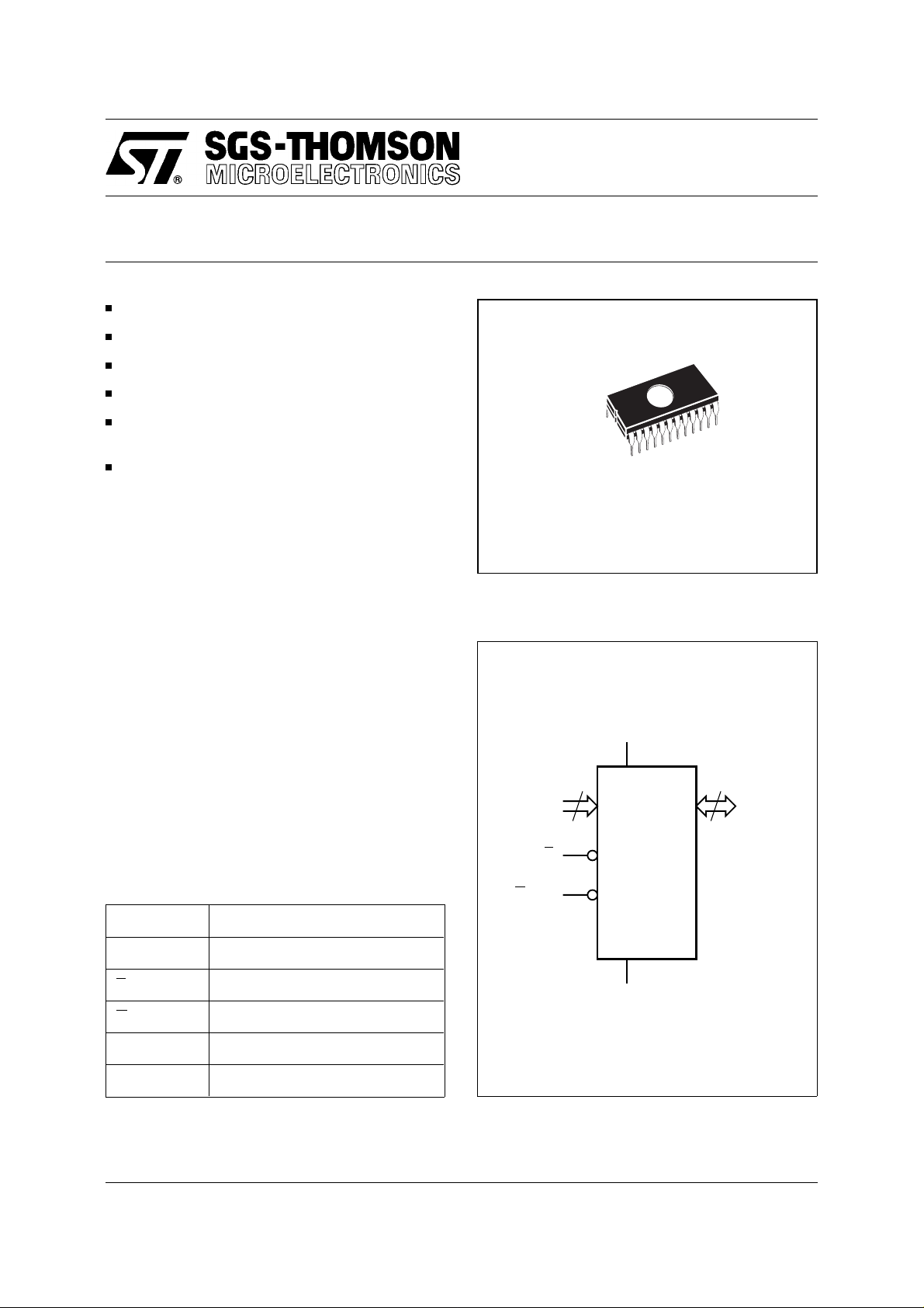
The M2732A is honsed in a 24 pin Window Ceramic
Frit-Seal Dual-in-Line pac kage. The transparent lid
allows the user to expose the chip t o ultraviolet light
to erase the bit patt ern. A new pattern can be then
written to the cleric e by following t he programmi ng
procedure.
M2732A
NMOS 32K (4K x 8) UV EPROM
24
1
FDIP24W (F)
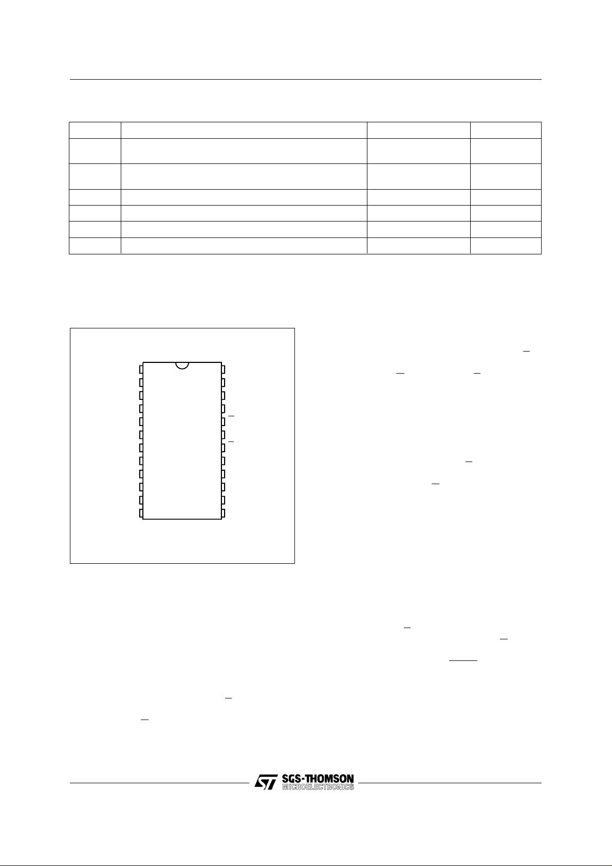
Figure 1. Logic Diag ra m
V
CC
12
A0-A11 Q0-Q7
8
E
T able 1. Signal Names
A0 - A11 Address Inputs
Q0 - Q7 Data Outputs
E Chip Enable
GV
PP
V
CC
V
SS
July 1994 1/9
Output Enable / Program Supply
Supply Voltage
Ground
GV
PP
M2732A
V
SS
AI00780B
Page 2
M2732A
Tab le 2. Absol ute Maxim u m Ratin gs
Symbol Parameter Value Unit
T
A
T
BIAS
T
STG
V
IO
V
CC
V
PP
Note: Except for the rating "Operating T emperature R ange", stresses above those lis ted in the Table "Absolute Maximum Ratings" may cause
permanent damage to the device. These are stress ratings only and opera tion of the device at these or any other conditions above those
indicated in the Operating sections of this specification is not implied. Exposure to Absolute Maximum Rati ng conditions for extended periods
may affect device reliabil ity. Refer also to the SGS-THOMSON SURE Program and other relevant quality documents.
Ambient Operating Temperature grade 1
grade 6
Temperature Under Bias grade 1
grade 6
Storage Temperature –65 to 125 °C
Input or Output Voltages –0.6 to 6 V
Supply Voltage –0.6 to 6 V
Program Supply Voltage –0.6 to 22 V
0 to 70
–40 to 85
–10 to 80
–50 to 95
°C
°C
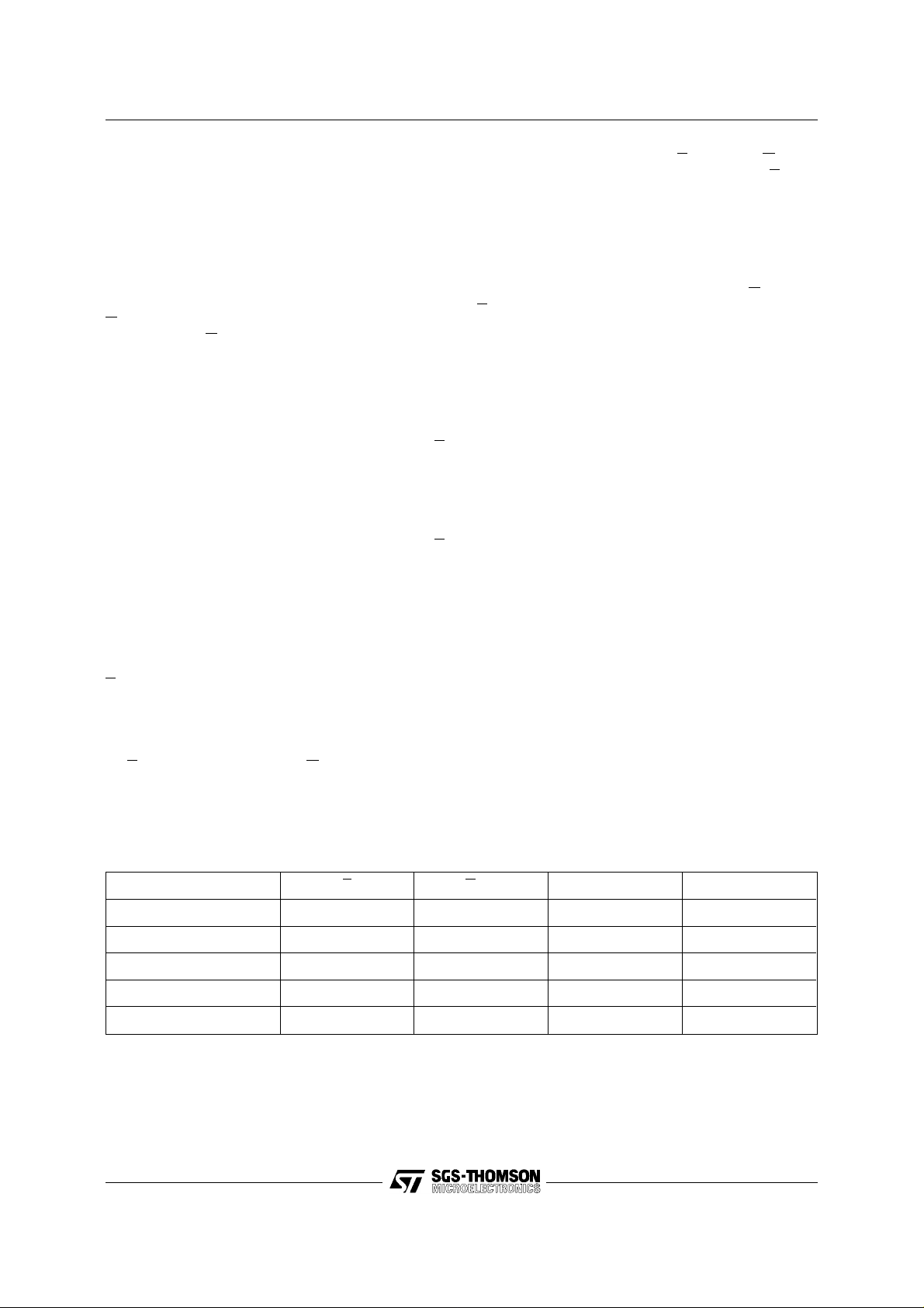
Figure 2. DIP Pin Connecti ons
A7
1
2
A6
3
A5
A4
4
5
A3
6
A2
A1
A0
Q0
Q1
Q2
V
SS
M2732A
7
8
9
10
11
12
24
23
22
21
20
19
18
17
16
15
14
13
AI00781
V
CC
A8
A9
A11
GV
A10
E
Q7
Q6
Q5
Q4
Q3
PP
DEVICE OPER ATION
The six modes of operation for the M2732A are
listed in the Operating Modes Table. A single 5V
power supply is required in the read mode. All
inputs are TTL level except for V
PP.
Read Mode
The M2732A has two control functions, both of
which must be logically satisfied in order to obtai n
data at the outputs. Chip Enable (
E) is the power
control and should be used for device selection.
Output Enable (
G) is the output control and should
be used to gate data to the output pins, independent of device selection.
Assuming that the addresses are stable, address
access time (t
output (t
ELQV
the falling edge of
) is equal to the delay fr om E to
AVAQ
). Data is available at the outputs after
G, assuming that E has been low
and the addresses have been stable for at least
t
AVQ V-tGLQV
.
Stand by Mod e
The M2732A has a standby mode which reduces
the active power current by 70 %, from 125 mA to
35 mA. The M2732A is placed in the sta ndby mode
by applying a TTL high signal to
E input. When in
standby mode, the outputs are in a high impedance
state, independent of the
GVPP input.
Two Line Output Control
Because M2732A ’s are usually used in larger memory arrays, this product features a 2 line control
function which accommodates the use of multiple
memory connection. The two line control function
allows:
a. the lowest possible memory power dissipation,
b. complete assurance that output bus content i on
will not occur.
To most efficiently use these two control lines, it is
recommended that
primary device selecting function, while
E be decoded and used as the
G should
be made a common connection to all devices in the
array and connected to the
READ line from the
system control bus.
This ensures that all deselected memory devices
are in their low power standby mode and that the
output pins are only active when data is required
from a particular memory device.
2/9
Page 3
M2732A
Programmin g
When delivered, and after each erasure, all bits of
the M2732A are in the “1" state. Data is introduce d
by selectively programming ”0’s" into the desired
bit locations. Although only “0’s” will be programmed, both “1’s” a nd “0’s” c an be present ed in
the data word. The only way to change a “0" to a
”1" is by ultraviolet light erasure.
The M2732A is in the programming mode when the
GVPP input is at 21V. A 0.1µF capacitor must be
placed across
GVPP and ground to suppress spurious voltage transients which may damage the
device. The data to be programmed is applied, 8
bits in parallel, to the data output pins. The levels
required for the address and data inputs are TTL.
When the address and data are stable, a 50ms,
active low, TTL program pulse is applied to the
input. A program pulse must be applied at each
address location to be programmed. Any location
can be programmed at any time - either individually ,
sequentially, or at random. T he program pulse has
a maximum width of 55ms. The M2732A must not
be programmed with a DC signal applied to the
input.
Programming of multiple M2732As in parallel with
the same data can be easily accomplished due to
the simplicity of the programming requirements.
Inputs of the paralleled M2732As may be connected together when they are programmed with
the same data. A low level TTL pulse applied to the
E input programs the paralleled 2732As.
Program Inhibit
Programming of multiple M2732As in parallel with
different data is also easily accomplished. Except
for
E, all like inputs (including GVPP) of the parallel
M2732As may be common. A T TL level program
pulse applied to a M2732A’s
E input with GV
21V will program that M2732A. A high level
inhibits the other M2732As from being programmed.
Program Verify
A verify should be performed on the programmed
bits to determine that they were correctly programmed. The verify is carried out with
E at VIL.
ERASURE OPERATION
The erasure characteristics of the M2732A are
such that erasure begins when the cells are exposed to light with wavelengths shorter than approximately 4000 Å. It should be noted that sunlight
and certain types of fluorescent lamps have wavelengths in the 3000-4000 Å range. Research shows
E
that constant exposure to room level fluorescent
lighting could erase a typical M2732A in approximately 3 years, while it would take approximately
1 week to cause erasure when exposed to the
direct sunlight. If the M2732A is to be exposed to
these types of lighting conditions for extended pe-
E
riods of time, it is suggested that opaque labels be
put over the M2732A window to prevent unintentional erasure.
The recommended erasure procedure for the
M2732A is exposure to shortwave ultraviolet light
which has a wavelength of 2537 Å. The integrated
dose (i.e. UV intensity x exposure time) for erasure
should be a minimum of 15 W-sec/cm
sure time with this dosage is approximately 15 to
20 minutes using an ultraviolet lamp with 12000
µW/cm
2
power rating. The M2732A should be
placed within 2.5 cm of the lamp tubes during
erasure. Some lamps have a filter on their tubes
which should be removed before erasure.
PP
E input
GVPP and
2
. The era-
at
T ab le 3. Operating Modes
Mode E GV
Read V
Program VIL Pulse V
Verify V
Program Inhibit V
Standby V
Note: X = VIH or VIL.
IL
IL
IH
IH
PP
V
IL
PP
V
IL
V
PP
XVCCHi-Z
V
CC
V
CC
V
CC
V
CC
V
CC
Q0 - Q7
Data Out
Data In
Data Out
Hi-Z
3/9
Page 4

M2732A
AC MEASUREMENT CONDITIONS
Input Rise and Fall Times ≤ 20ns
Figure 4. AC T esti ng Load Circui t
1.3V
Input Pulse Voltages 0.45V to 2.4V
Input and Output Timing Ref. Voltages 0.8V to 2.0V
1N914
Note that Output Hi-Z is defined as the point where data
is no longer driven.
Figure 3. AC Test ing Input Outp ut W avefo rm s
3.3kΩ
DEVICE
UNDER
2.4V
0.45V
T ab le 4. Capacitance
(1)
(TA = 25 °C, f = 1 MHz )
2.0V
0.8V
AI00827
Symbol Parameter Test Condition Min Max Unit
C
IN
C
IN1
Input Capacitance (except GVPP)V
Input Capacitance (GVPP)V
TEST
CL = 100pF
CL includes JIG capacitance
= 0V 6 pF
IN
= 0V 20 pF
IN
OUT
AI00828
C
OUT
Note: 1. Sampled only, not 100% tested.
Output Capacitance V
Figure 5. Read Mode AC Wavefor m s
A0-A11
tAVQV
E
G
tELQV
Q0-Q7
tGLQV
VALID
= 0V 12 pF
OUT
tAXQX
tEHQZ
tGHQZ
DATA OUT
Hi-Z
AI00782
4/9
Page 5

M2732A
Tab l e 5. Read Mode DC Characteristics
(1)
(TA = 0 to 70 °C or –40 to 85 °C; VCC = 5V ± 5% or 5V ± 10%; VPP = VCC)
Symbol Parameter Test Condition
I
LI
I
LO
I
CC
I
CC1
V
V
V
OL
V
OH
Note: 1. VCC must be applied simultaneously with or bef o re VPP and removed simultaneously or after VPP.
Tab l e 6. Read Mode AC Characterist ics
Input Leakage Current 0 ≤ VIN ≤ V
Output Leakage Current V
OUT
Supply Current E = VIL, G = V
Supply Current (Standby) E = VIH, G = V
Input Low Voltage –0.1 0.8 V
IL
Input High Voltage 2 VCC + 1 V
IH
= V
CC
CC
IL
IL
Output Low Voltage IOL = 2.1mA 0.45 V
Output High Voltage IOH = –400µA 2.4 V
(1)
Min Max
(TA = 0 to 70 °C or –40 to 85 °C; VCC = 5V ± 5% or 5V ± 10%; VPP = VCC)
Symbol Alt Parameter
Test
Condition
-2, -20 blank, -25 -3 -4
Min Max Min Max Min Max Min Max
Address Valid to
t
AVQV
t
ELQV
t
GLQV
t
EHQZ
t
GHQZ
t
AXQX
Notes: 1. VCC must be applied simultaneously with or befo re VPP and removed simultaneously or after VPP.
t
ACC
Output Valid
Chip Enable Low to
t
CE
Output Valid
Output Enable Low
t
OE
to Output Valid
(2)
(2)
2. Sampled only, not 100% tested.
Chip Enable High to
t
DF
Output Hi-Z
Output Enable High
t
DF
to Output Hi-Z
Address Transition to
t
OH
Output Transition
E = VIL,
G = V
G = V
E = V
G = V
E = V
E = VIL,
G = V
IL
IL
IL
IL
IL
IL
200 250 300 450 ns
200 250 300 450 ns
100 100 150 150 ns
0 60 0 60 0 130 0 130 ns
0 60 0 60 0 130 0 130 ns
0000ns
M2732A
Value
Unit
±10 µA
±10 µA
125 mA
35 mA
Unit
5/9
Page 6

M2732A
Tab le 7. Programmin g Mode DC Characteristics
(1)
(TA = 25 °C; VCC = 5V ± 5%; VPP = 21V ± 0.5V)
Symbol Parameter Test Condition Min Max Units
I
LI
I
CC
I
PP
V
IL
V
IH
V
OL
V
OH
Note: 1. VCC must be applied simultaneously with or before VPP and removed simultaneously or after VPP.
T ab le 8. Programming Mod e AC Charact eristics
Input Leakage Current VIL ≤ VIN ≤ V
Supply Current E = VIL, G = V
Program Current E = VIL, G = V
IH
IL
PP
±10 µA
125 mA
30 mA
Input Low Voltage –0.1 0.8 V
Input High Voltage 2 VCC + 1 V
Output Low Voltage IOL = 2.1mA 0.45 V
Output High Voltage IOH = –400µA 2.4 V
(1)
(TA = 25 °C; VCC = 5V ± 5%; VPP = 21V ± 0.5V)
Symbol Alt Parameter Test Condition Min Max Units
t
AVEL
t
QVEL
t
VPHEL
t
VPL1VPL2
t
ELEH
t
EHQX
t
EHVPX
t
t
t
OES
t
PRT
t
t
t
OEH
Address Valid to Chip Enable
AS
Low
Input Valid to Chip Enable Low 2 µs
DS
VPP High to Chip Enable Low 2 µs
VPP Rise Time 50 ns
Chip Enable Program Pulse
PW
Width
Chip Enable High to Input
DH
Transition
Chip Enable High to V
PP
Transition
2 µs
45 55 ms
2 µs
2 µs
t
VPLEL
t
ELQV
t
EHQZ
t
EHAX
Note: 1. VCC must be applied simultaneously with or before VPP and removed simultaneously or after VPP.
t
t
t
t
VPP Low to Chip Enable Low 2 µs
VR
Chip Enable Low to Output
DV
Valid
Chip Enable High to Output
DF
Hi-Z
Chip Enable High to Address
AH
Transition
E = VIL, G = V
IL
0 130 ns
0ns
6/9
1 µs
Page 7

Figure 6. Programming and Verify Modes AC Waveform s
M2732A
A0-A11
tAVEL
Q0-Q7
GV
PP
E
tQVEL
tVPHEL
DATA IN
ORDERI NG INFO RM ATION SCHEME
Example: M2732A -2 F 1
tELEH
PROGRAM
VALID
tEHQX
tEHVPX
tVPLEL
DATA OUT
tELQV
VERIFY
tEHAX
tEHQZ
AI00783
Speed and VCC Tolerance
-2 200 ns, 5V ±5%
blank 250 ns, 5V ±5%
Package
F FDIP24W
Temperature Range
1 0 to 70 °C
6 –40 to 85 °C
-3 300 ns, 5V ±5%
-4 450 ns, 5V ±5%
-20 200 ns, 5V ±10%
-25 250 ns, 5V ±10%
For a list of available options (Speed, VCC T olerance, Package, etc ...) refer to the current Memory S hortform
catalogue.
For further information o n any aspect of this device, please contact SGS-THOMSO N Sales Office nearest
to you.
7/9
Page 8

M2732A
FDIP24W - 24 pin Ceramic Frit-seal DIP, with window
Symb
Typ Min Max Typ Min Max
A 5.71 0.225
A1 0.50 1.78 0.020 0.070
A2 3.90 5.08 0.154 0.200
B 0.40 0.55 0.016 0.022
B1 1.17 1.42 0.046 0.056
C 0.22 0.31 0.009 0.012
D 32.30 1.272
E 15.40 15.80 0.606 0.622
E1 13.05 13.36 0.514 0.526
e1 2.54 – – 0.100 – –
e3 27.94 – – 1.100 – –
eA 16.17 18.32 0.637 0.721
L 3.18 4.10 0.125 0.161
S 1.52 2.49 0.060 0.098
∅ 7.11 – – 0.280 – –
α 4° 15° 4° 15°
N24 24
FDIP24W
mm inches
Drawing is not to scale
8/9
A1AL
B1 B e1
e3
D
S
N
∅
1
A2
Cα
eA
E1 E
FDIPW-a
Page 9

M2732A
Information furnished is believed to be accurate and reliable. However, SGS-THOMSON Microelectronics assumes no responsibility for the
consequences of use of such information nor for any infringement of patents or other rights of third parties which may result from its use. No
license is granted by implication or otherwise under any patent or patent rights of SGS-THOMSON Microelectronics. Specificat ions mentioned
in this publication are subject to change without notice. This publication supersedes and replaces all information previously supplied.
SGS-THOMSON Microelectronics products are not authorized for use as critical components in life support devices or systems without express
written approval of SGS-THOMSON Microelectronics.
© 1994 SGS-THOMSON Microelectronics - All Rights Reserved
Australia - Brazil - China - France - Germany - Hong Kong - Italy - Japan - Korea - Malaysia - Malta - Morocc o - The Netherlands -
Singapore - Spain - Sweden - Switzerland - Taiwan - Thailand - United Kingdom - U.S.A.
SGS-THOMSON Microelectronics GROUP OF COMPANIES
9/9
 Loading...