

Page 1
32-Mbit, dual I/O, 4-Kbyte subsector erase,
serial Flash memory with 75 MHz SPI bus interface
Features
■ SPI bus compatible serial interface
■ 75 MHz (maximum) clock frequency
■ 2.7 V to 3.6 V single supply voltage
■ Dual input/output instructions resulting in an
equivalent clock frequency of 150 MHz:
– Dual Output Fast Read instruction
– Dual Input Fast Program instruction
■ 32 Mbit Flash memory
– Uniform 4-Kbyte subsectors
– Uniform 64-Kbyte sectors
■ Additional 64-byte user-lockable, one-time
programmable (OTP) area
■ Erase capability
– Subsector (4-Kbyte) granularity
– Sector (64-Kbyte) granularity
– Bulk Erase (32 Mbit) in 17 s (typical with
V
= 9 V)
PP
■ Write protections
– Software write protection applicable to
every 64-Kbyte sector (volatile lock bit)
– Har dware write protection: protected area
size defined by three non- volatile bit s (BP0,
BP1 and BP2)
■ Deep Power-down mode: 5 µA (typical)
■ Electronic signature
– JEDEC standard two-byte signature
(7116h)
– Unique ID code (UID) +16 byte of CFI data
■ More than 100 000 write cycles per sector
■ More than 20 year data retention
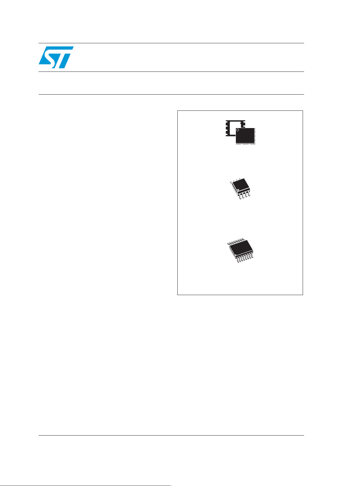
■ Packages
– ECOPACK® (RoHS compliant)
M25PX32
VFQFPN8 (MP)
6 × 5 mm
SO8W (MW)
208 mils
SO16 (MF)
300 mils
September 2007 Rev 4 1/63
www.st.com
1
Page 2

Contents M25PX32
Contents
1 Description . . . . . . . . . . . . . . . . . . . . . . . . . . . . . . . . . . . . . . . . . . . . . . . . . 6
2 Signal descriptions . . . . . . . . . . . . . . . . . . . . . . . . . . . . . . . . . . . . . . . . . . 9
2.1 Serial Data output (DQ1) . . . . . . . . . . . . . . . . . . . . . . . . . . . . . . . . . . . . . . 9
2.2 Serial Data input (DQ0) . . . . . . . . . . . . . . . . . . . . . . . . . . . . . . . . . . . . . . . 9
2.3 Serial Clock (C) . . . . . . . . . . . . . . . . . . . . . . . . . . . . . . . . . . . . . . . . . . . . . 9
2.4 Chip Select (S
2.5 Hold (HOLD
2.6 Write Protect/Enhanced Program supply voltage (W
2.7 V
2.8 V
supply voltage . . . . . . . . . . . . . . . . . . . . . . . . . . . . . . . . . . . . . . . . . . 10
CC
ground . . . . . . . . . . . . . . . . . . . . . . . . . . . . . . . . . . . . . . . . . . . . . . . . 10
SS
) . . . . . . . . . . . . . . . . . . . . . . . . . . . . . . . . . . . . . . . . . . . . . . 9
) . . . . . . . . . . . . . . . . . . . . . . . . . . . . . . . . . . . . . . . . . . . . . . . . 9
/VPP) . . . . . . . . . . . . 10
3 SPI modes . . . . . . . . . . . . . . . . . . . . . . . . . . . . . . . . . . . . . . . . . . . . . . . . 11
4 Operating features . . . . . . . . . . . . . . . . . . . . . . . . . . . . . . . . . . . . . . . . . 13
4.1 Page programming . . . . . . . . . . . . . . . . . . . . . . . . . . . . . . . . . . . . . . . . . . 13
4.2 Dual Input Fast Program . . . . . . . . . . . . . . . . . . . . . . . . . . . . . . . . . . . . . 13
4.3 Subsector Erase, Sector Erase and Bulk Erase . . . . . . . . . . . . . . . . . . . . 13
4.4 Polling during a Write, Program or Erase cycle . . . . . . . . . . . . . . . . . . . . 13
4.5 Fast Bulk Erase mode . . . . . . . . . . . . . . . . . . . . . . . . . . . . . . . . . . . . . . . 14
4.6 Active Power, Standby Power and Deep Power-down modes . . . . . . . . . 14
4.7 Status Register . . . . . . . . . . . . . . . . . . . . . . . . . . . . . . . . . . . . . . . . . . . . . 14
4.8 Protection modes . . . . . . . . . . . . . . . . . . . . . . . . . . . . . . . . . . . . . . . . . . . 15
4.8.1 Protocol-related protections . . . . . . . . . . . . . . . . . . . . . . . . . . . . . . . . . . 15
4.8.2 Specific hardware and software protection . . . . . . . . . . . . . . . . . . . . . . 16
4.9 Hold condition . . . . . . . . . . . . . . . . . . . . . . . . . . . . . . . . . . . . . . . . . . . . . . 18
5 Memory organization . . . . . . . . . . . . . . . . . . . . . . . . . . . . . . . . . . . . . . . 19
6 Instructions . . . . . . . . . . . . . . . . . . . . . . . . . . . . . . . . . . . . . . . . . . . . . . . 23
6.1 Write Enable (WREN) . . . . . . . . . . . . . . . . . . . . . . . . . . . . . . . . . . . . . . . 25
6.2 Write Disable (WRDI) . . . . . . . . . . . . . . . . . . . . . . . . . . . . . . . . . . . . . . . . 26
2/63
Page 3

M25PX32 Contents
6.3 Read Identification (RDID) . . . . . . . . . . . . . . . . . . . . . . . . . . . . . . . . . . . . 27
6.4 Read Status Register (RDSR) . . . . . . . . . . . . . . . . . . . . . . . . . . . . . . . . . 28
6.4.1 WIP bit . . . . . . . . . . . . . . . . . . . . . . . . . . . . . . . . . . . . . . . . . . . . . . . . . . 28
6.4.2 WEL bit . . . . . . . . . . . . . . . . . . . . . . . . . . . . . . . . . . . . . . . . . . . . . . . . . 28
6.4.3 BP2, BP1, BP0 bits . . . . . . . . . . . . . . . . . . . . . . . . . . . . . . . . . . . . . . . . 28
6.4.4 TB bit . . . . . . . . . . . . . . . . . . . . . . . . . . . . . . . . . . . . . . . . . . . . . . . . . . . 29
6.4.5 SRWD bit . . . . . . . . . . . . . . . . . . . . . . . . . . . . . . . . . . . . . . . . . . . . . . . . 29
6.5 Write Status Register (WRSR) . . . . . . . . . . . . . . . . . . . . . . . . . . . . . . . . . 30
6.6 Read Data Bytes (READ) . . . . . . . . . . . . . . . . . . . . . . . . . . . . . . . . . . . . . 32
6.7 Read Data Bytes at higher speed (FAST_READ) . . . . . . . . . . . . . . . . . . 33
6.8 Dual Output Fast Read (DOFR) . . . . . . . . . . . . . . . . . . . . . . . . . . . . . . . . 34
6.9 Read Lock Register (RDLR) . . . . . . . . . . . . . . . . . . . . . . . . . . . . . . . . . . . 35
6.10 Read OTP (ROTP) . . . . . . . . . . . . . . . . . . . . . . . . . . . . . . . . . . . . . . . . . . 36
6.11 Page Program (PP) . . . . . . . . . . . . . . . . . . . . . . . . . . . . . . . . . . . . . . . . . 37
6.12 Dual Input Fast Program (DIFP) . . . . . . . . . . . . . . . . . . . . . . . . . . . . . . . . 39
6.13 Program OTP instruction (POTP) . . . . . . . . . . . . . . . . . . . . . . . . . . . . . . . 41
6.14 Write to Lock Register (WRLR) . . . . . . . . . . . . . . . . . . . . . . . . . . . . . . . . 43
6.15 Subsector Erase (SSE) . . . . . . . . . . . . . . . . . . . . . . . . . . . . . . . . . . . . . . 44
6.16 Sector Erase (SE) . . . . . . . . . . . . . . . . . . . . . . . . . . . . . . . . . . . . . . . . . . 45
6.17 Bulk Erase (BE) . . . . . . . . . . . . . . . . . . . . . . . . . . . . . . . . . . . . . . . . . . . . 46
6.18 Deep Power-down (DP) . . . . . . . . . . . . . . . . . . . . . . . . . . . . . . . . . . . . . . 47
6.19 Release from Deep Power-down (RDP) . . . . . . . . . . . . . . . . . . . . . . . . . . 48
7 Power-up and power-down . . . . . . . . . . . . . . . . . . . . . . . . . . . . . . . . . . . 49
8 Initial delivery state . . . . . . . . . . . . . . . . . . . . . . . . . . . . . . . . . . . . . . . . . 51
9 Maximum rating . . . . . . . . . . . . . . . . . . . . . . . . . . . . . . . . . . . . . . . . . . . . 51
10 DC and AC parameters . . . . . . . . . . . . . . . . . . . . . . . . . . . . . . . . . . . . . . 52
11 Package mechanical . . . . . . . . . . . . . . . . . . . . . . . . . . . . . . . . . . . . . . . . 58
12 Part numbering . . . . . . . . . . . . . . . . . . . . . . . . . . . . . . . . . . . . . . . . . . . . 61
13 Revision history . . . . . . . . . . . . . . . . . . . . . . . . . . . . . . . . . . . . . . . . . . . 62
3/63
Page 4

List of tables M25PX32
List of tables
Table 1. Signal names . . . . . . . . . . . . . . . . . . . . . . . . . . . . . . . . . . . . . . . . . . . . . . . . . . . . . . . . . . . . 7
Table 2. Software protection truth table (Sectors 0 to 63, 64 Kbyte granularity) . . . . . . . . . . . . . . . 16
Table 3. Protected area sizes. . . . . . . . . . . . . . . . . . . . . . . . . . . . . . . . . . . . . . . . . . . . . . . . . . . . . . 17
Table 4. Memory organization . . . . . . . . . . . . . . . . . . . . . . . . . . . . . . . . . . . . . . . . . . . . . . . . . . . . . 20
Table 5. Instruction set . . . . . . . . . . . . . . . . . . . . . . . . . . . . . . . . . . . . . . . . . . . . . . . . . . . . . . . . . . . 24
Table 6. Read Identification (RDID) data-out sequence. . . . . . . . . . . . . . . . . . . . . . . . . . . . . . . . . . 27
Table 7. Status Register format . . . . . . . . . . . . . . . . . . . . . . . . . . . . . . . . . . . . . . . . . . . . . . . . . . . . 28
Table 8. Protection modes . . . . . . . . . . . . . . . . . . . . . . . . . . . . . . . . . . . . . . . . . . . . . . . . . . . . . . . . 31
Table 9. Lock Register out . . . . . . . . . . . . . . . . . . . . . . . . . . . . . . . . . . . . . . . . . . . . . . . . . . . . . . . . 35
Table 10. Lock Register in . . . . . . . . . . . . . . . . . . . . . . . . . . . . . . . . . . . . . . . . . . . . . . . . . . . . . . . . . 43
Table 11. Power-up timing and VWI threshold . . . . . . . . . . . . . . . . . . . . . . . . . . . . . . . . . . . . . . . . . . 50
Table 12. Absolute maximum ratings . . . . . . . . . . . . . . . . . . . . . . . . . . . . . . . . . . . . . . . . . . . . . . . . . 51
Table 13. Operating conditions. . . . . . . . . . . . . . . . . . . . . . . . . . . . . . . . . . . . . . . . . . . . . . . . . . . . . . 52
Table 14. AC measurement conditions. . . . . . . . . . . . . . . . . . . . . . . . . . . . . . . . . . . . . . . . . . . . . . . . 5 2
Table 15. Capacitance . . . . . . . . . . . . . . . . . . . . . . . . . . . . . . . . . . . . . . . . . . . . . . . . . . . . . . . . . . . . 52
Table 16. DC characteristics. . . . . . . . . . . . . . . . . . . . . . . . . . . . . . . . . . . . . . . . . . . . . . . . . . . . . . . . 53
Table 17. AC characteristics. . . . . . . . . . . . . . . . . . . . . . . . . . . . . . . . . . . . . . . . . . . . . . . . . . . . . . . . 54
Table 18. VFQFPN8 (MLP8) 8-lead very thin fine pitch quad flat package no lead,
6 × 5 mm, package mechanical data . . . . . . . . . . . . . . . . . . . . . . . . . . . . . . . . . . . . . . . . . 58
Table 19. SO8W 8-lead plastic small outline, 208 mils body width, package
mechanical data. . . . . . . . . . . . . . . . . . . . . . . . . . . . . . . . . . . . . . . . . . . . . . . . . . . . . . . . . 5 9
Table 20. SO16 wide - 16-lead plastic small outline, 300 mils body width, mechanical data. . . . . . . 60
Table 21. Ordering information scheme . . . . . . . . . . . . . . . . . . . . . . . . . . . . . . . . . . . . . . . . . . . . . . . 61
Table 22. Document revision history . . . . . . . . . . . . . . . . . . . . . . . . . . . . . . . . . . . . . . . . . . . . . . . . . 62
4/63
Page 5

M25PX32 List of figures
List of figures
Figure 1. Logic diagram . . . . . . . . . . . . . . . . . . . . . . . . . . . . . . . . . . . . . . . . . . . . . . . . . . . . . . . . . . . . 7
Figure 2. VFQFPN and SO8 connections . . . . . . . . . . . . . . . . . . . . . . . . . . . . . . . . . . . . . . . . . . . . . . 7
Figure 3. SO16 connections . . . . . . . . . . . . . . . . . . . . . . . . . . . . . . . . . . . . . . . . . . . . . . . . . . . . . . . . 8
Figure 4. Bus Master and memory devices on the SPI bus. . . . . . . . . . . . . . . . . . . . . . . . . . . . . . . . 11
Figure 5. SPI modes supported . . . . . . . . . . . . . . . . . . . . . . . . . . . . . . . . . . . . . . . . . . . . . . . . . . . . . 12
Figure 6. Hold condition activation. . . . . . . . . . . . . . . . . . . . . . . . . . . . . . . . . . . . . . . . . . . . . . . . . . . 18
Figure 7. Block diagram. . . . . . . . . . . . . . . . . . . . . . . . . . . . . . . . . . . . . . . . . . . . . . . . . . . . . . . . . . . 19
Figure 8. Write Enable (WREN) instruction sequence. . . . . . . . . . . . . . . . . . . . . . . . . . . . . . . . . . . . 25
Figure 9. Write Disable (WRDI) instruction sequence . . . . . . . . . . . . . . . . . . . . . . . . . . . . . . . . . . . . 26
Figure 10. Read Identification (RDID) instruction sequence and data-out sequence . . . . . . . . . . . . . 27
Figure 11. Read Status Register (RDSR) instruction sequence and data-out sequence . . . . . . . . . . 29
Figure 12. Write Status Register (WRSR) instruction sequence . . . . . . . . . . . . . . . . . . . . . . . . . . . . . 30
Figure 13. Read Data Bytes (READ) instruction sequence and data-out sequence . . . . . . . . . . . . . . 32
Figure 14. Read Data Bytes at higher speed (FAST_READ) instruction sequence
and data-out sequence . . . . . . . . . . . . . . . . . . . . . . . . . . . . . . . . . . . . . . . . . . . . . . . . . . . . 33
Figure 15. Dual Output Fast Read instruction sequence . . . . . . . . . . . . . . . . . . . . . . . . . . . . . . . . . . . 34
Figure 16. Read Lock Register (RDLR) instruction sequence and data-out sequence . . . . . . . . . . . . 35
Figure 17. Read OTP (ROTP) instruction and data-out sequence . . . . . . . . . . . . . . . . . . . . . . . . . . . 36
Figure 18. Page Program (PP) instruction sequence . . . . . . . . . . . . . . . . . . . . . . . . . . . . . . . . . . . . . 38
Figure 19. Dual Input Fast Program (DIFP) instruction sequence . . . . . . . . . . . . . . . . . . . . . . . . . . . . 40
Figure 20. Program OTP (POTP) instruction sequence . . . . . . . . . . . . . . . . . . . . . . . . . . . . . . . . . . . 42
Figure 21. How to permanently lock the 64 OTP bytes . . . . . . . . . . . . . . . . . . . . . . . . . . . . . . . . . . . . 42
Figure 22. Write to Lock Register (WRLR) instruction sequence. . . . . . . . . . . . . . . . . . . . . . . . . . . . . 43
Figure 23. Subsector Erase (SSE) instruction sequence. . . . . . . . . . . . . . . . . . . . . . . . . . . . . . . . . . . 44
Figure 24. Sector Erase (SE) instruction sequence. . . . . . . . . . . . . . . . . . . . . . . . . . . . . . . . . . . . . . . 45
Figure 25. Bulk Erase (BE) instruction sequence . . . . . . . . . . . . . . . . . . . . . . . . . . . . . . . . . . . . . . . . 46
Figure 26. Deep Power-down (DP) instruction sequence . . . . . . . . . . . . . . . . . . . . . . . . . . . . . . . . . . 47
Figure 27. Release from Deep Power-down (RDP) instruction sequence. . . . . . . . . . . . . . . . . . . . . . 48
Figure 28. Power-up timing . . . . . . . . . . . . . . . . . . . . . . . . . . . . . . . . . . . . . . . . . . . . . . . . . . . . . . . . . 50
Figure 29. AC measurement I/O waveform . . . . . . . . . . . . . . . . . . . . . . . . . . . . . . . . . . . . . . . . . . . . . 52
Figure 30. Serial input timing . . . . . . . . . . . . . . . . . . . . . . . . . . . . . . . . . . . . . . . . . . . . . . . . . . . . . . . . 55
Figure 31. Write Protect Setup and Hold timing during WRSR when SRWD=1 . . . . . . . . . . . . . . . . . 56
Figure 32. Hold timing . . . . . . . . . . . . . . . . . . . . . . . . . . . . . . . . . . . . . . . . . . . . . . . . . . . . . . . . . . . . . 56
Figure 33. Output timing . . . . . . . . . . . . . . . . . . . . . . . . . . . . . . . . . . . . . . . . . . . . . . . . . . . . . . . . . . . 57
Figure 34. V
Figure 35. VFQFPN8 (MLP8) 8-lead very thin fine pitch quad flat package no lead,
Figure 36. SO8W 8-lead plastic small outline, 208 mils body width, package outline. . . . . . . . . . . . . 59
Figure 37. SO16 wide - 16-lead plastic small outline, 300 mils body width, package outline . . . . . . . 60
timing. . . . . . . . . . . . . . . . . . . . . . . . . . . . . . . . . . . . . . . . . . . . . . . . . . . . . . . . . . . . . 57
PPH
6 × 5 mm, package outline . . . . . . . . . . . . . . . . . . . . . . . . . . . . . . . . . . . . . . . . . . . . . . . . . 58
5/63
Page 6

Description M25PX32
1 Description
The M25PX32 is a 32 Mbit (4 Mb x 8) serial Flash memory, with advanced write protection
mechanisms, accessed by a high speed SPI-compatible bus.
The M25PX32 supports two new, high-performance dual input/output instructions:
● Dual Output Fast Read (DOFR) instruction used to read data a t up t o 75 MHz by using
both pin DQ1 and pin DQ0 as outputs
● Dual Input Fast Program (DIFP) instruction used to program data at up to 75 MHz by
using both pin DQ1 and pin DQ0 as inputs
These new instructions double the transfer bandwidth for read and program operations.
The memory can be programmed 1 to 256 bytes at a time, using the Page Program
instruction.
The memory is organized as 64 sectors that are further divided into 16 subsectors each
(1024 subsectors in total).
The memory can be erased a 4-Kbyte subsector at a time, a 64-Kbyte sect or at a time , or as
a whole. It can be Write Protected by software using a mix of volatile and non-volatile
protection features, depending on the application needs. The protection granularity is of 64
Kbytes (sector granularity).
An enhanced Fast Bulk Erase mode is available to speed up Bulk Erase operations in
factory environment. The device enters this mode whenever the V
the Write Protect/Enhanced Program supply voltage pin (W
/VPP).
voltage is applied to
PPH
The M25PX32 has 64 One-Time-Programmable bytes (OTP bytes) that can be read and
programmed using two dedicated instructions, Read OTP (ROTP) and Program OTP
(POTP), respectively. These 64 bytes can be permanently locked by a particular Program
OTP (POTP) sequence. Once they have been lock ed, they become read-only and this state
cannot be reverted.
Further features are available as additional security options. More information on these
security features is available, upon completion of an NDA (nondisclosure agreement), and
are, therefore, not described in this datasheet. For more details of this option contact your
nearest ST Sales office.
In order to meet environmental requirements, ST offers the M25PX32 in ECOPACK®
packages. ECOPACK® packages are Lead-free and RoHS compliant.
ECOPACK® is an ST trademark. ECOPACK® specifications are available at: www.st.com.
6/63
Page 7
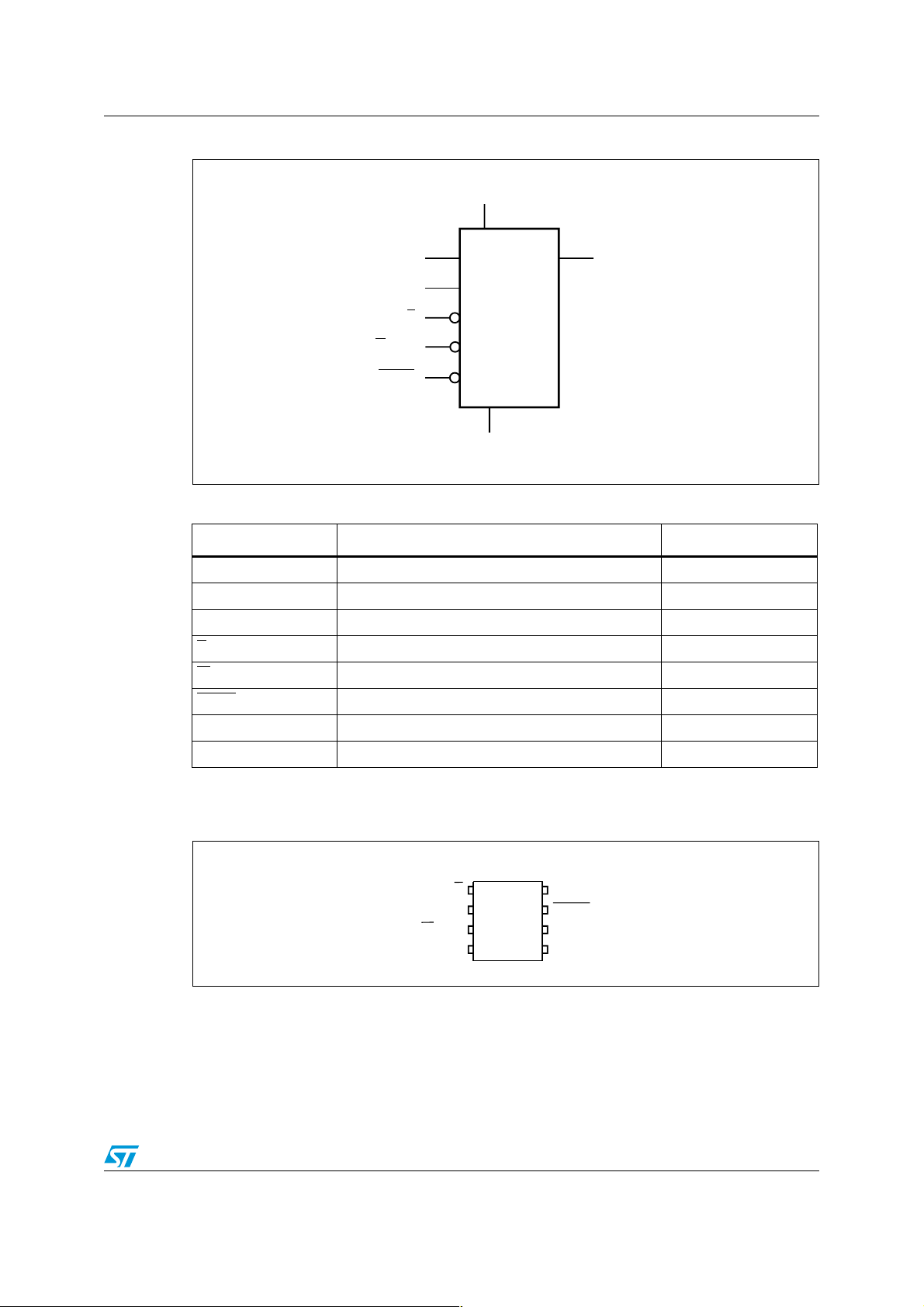
M25PX32 Description
Figure 1. Logic diagram
V
CC
DQ0
DQ1
C
M25PX32
W/V
S
PP
HOLD
V
Table 1. Signal names
SS
AI14228
Signal name Function Direction
C Serial Clock Input
DQ0 Serial Data input I/O
DQ1 Serial Data output I/O
(1)
(2)
S Chip Select Input
/V
W
PP
HOLD
Write Protect/Enhanced Program supply voltage Input
Hold Input
V
CC
V
SS
1. Serves as an output during Dual Output Fast Read (DOFR) instructions.
2. Serves as an input during Dual Input Fast Program (DIFP) instructions.
Supply voltage
Ground
Figure 2. VFQFPN and SO8 connections
M25PX32
SV
1
2
W/V
1. There is an exposed central pad on the underside of the VFQFPN package. This is pulled, internally, to
V
, and must not be allowed to be connected to any other voltage or signal line on the PCB.
SS
2. See Package mechanical section for package dimensions, and how to identify pin-1.
PP
SS
3
4
7/63
8
CC
7
HOLDDQ1
6
C
5
DQ0V
AI13720b
Page 8

Description M25PX32
Figure 3. SO16 connections
M25PX32
HOLD
V
CC
DU
DU
DU
S
DQ1
1. DU = Don’t use.
2. See Package mechanical section for package dimensions, and how to identify pin-1.
16
1
2
3
4
5
6
7
8
15
14
13
12
11
10
C
DQ0
DUDU
DU
DU
DU
V
SS
9
W/V
PP
AI13721b
8/63
Page 9

M25PX32 Signal descriptions
2 Signal descriptions
2.1 Serial Data output (DQ1)
This output signal is used to transf er data serially out of the device. Data are shifted out on
the falling edge of Serial Clock (C).
During the Dual Input Fast Program (DIFP) instruction, pin DQ1 is used as an input. It is
latched on the rising edge of the Serial Clock (C).
2.2 Serial Data input (DQ0)
This input signal is used to transfer data serially into the device. It receives instructions,
addresses, and the data to be programmed. Values are latched on the rising edge of Serial
Clock (C).
During the Dual Output Fast Read (DOFR) instruction, pin DQ0 is used as an output. Data
are shifted out on the falling edge of the Serial Clock (C).
2.3 Serial Clock (C)
This input signal provides the timing of the serial interface. Instructions, addresses, or data
present at Serial Data input (DQ0) are latched on the rising edge of Serial Clock (C). Data
on Serial Data output (DQ1) changes after the falling edge of Serial Clock (C).
2.4 Chip Select (S)
When this input signal is High, the device is deselec ted and Serial Data output (DQ1) is at
high impedance. Unless an internal Program, Erase or Write Status Register cycle is in
progress, the device will be in the Standby Power mode (this is not the Deep Power-down
mode). Driving Chip Select (S
After Power-up, a falling edge on Chip Select (S
instruction.
2.5 Hold (HOLD)
The Hold (HOLD) signal is used to pause any serial communications with the de vice without
deselecting the device.
During the Hold condition, the Serial Data output (DQ1) is hi gh impe dance, and Serial Data
input (DQ0) and Serial Clock (C) are Don’t care.
To start the Hold condition, the device must be selected, with Chip Select (S
) Low enables the device, placing it in the Active Power mode .
) is required prior to the start of any
) driven Low.
9/63
Page 10

Signal descriptions M25PX32
2.6 Write Protect/Enhanced Program supply voltage (W/VPP)
W/VPP is both a control input and a power supply p in. The two functions ar e selected by the
voltage range app lied to the pin.
If the W
input. This input signal is used to freeze the size of the area of memory that is protected
against program or erase instructions (as specified by the values in the BP2, BP1 and BP0
bits of the Status Register. See Table 9).
If V
during the Bulk Erase cycle. In this case V
completed.
/V
input is kept in a low voltage range (0 V to VCC) the pin is seen as a control
PP
is in the range of V
PP
PPH
2.7 VCC supply voltage
VCC is the supply voltage.
2.8 VSS ground
VSS is the reference for the VCC supply voltage.
(as defined in Table 14) it acts as an additional power supply
must be stable until the Bulk Er ase algorithm is
PP
10/63
Page 11
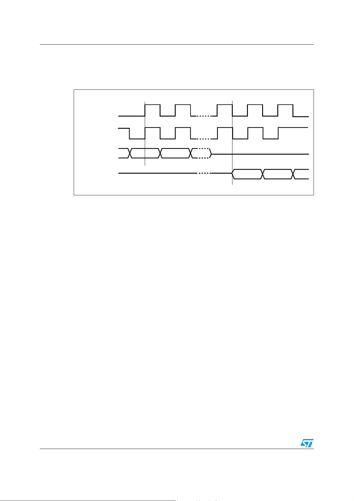
M25PX32 SPI modes
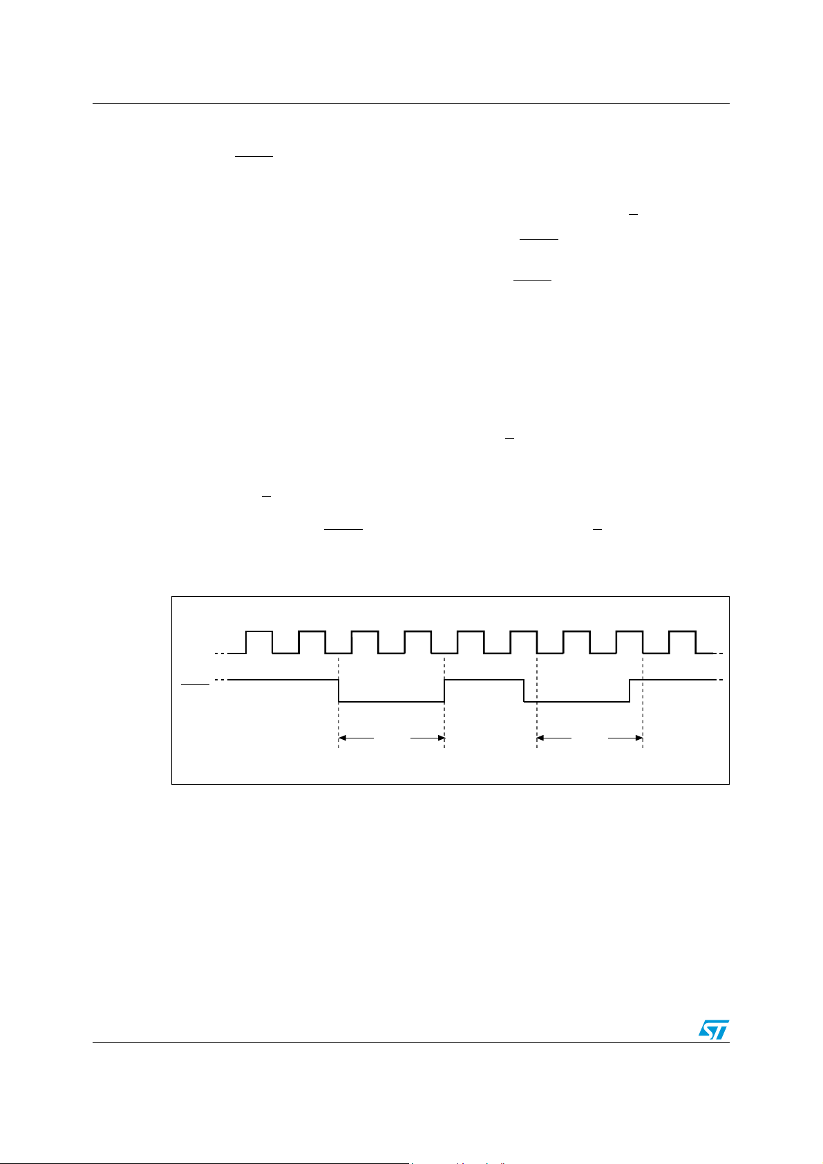
3 SPI modes
These devices can be drive n by a microcontroller with its SPI peripheral running in either of
the two following modes:
● CPOL=0, CPHA=0
● CPOL=1, CPHA=1
For these two modes, input data is latched in on the rising edge of Serial Clock (C), and
output data is available from the falling edge of Serial Clock (C).
The difference between the two modes, as sho wn in Figure 5, is the clock polarity when the
bus master is in Standby mode and not transferring data:
● C remains at 0 for (CPOL=0, CPHA=0)
● C remains at 1 for (CPOL=1, CPHA=1)
Figure 4. Bus Master and memory devices on the SPI bus
V
SS
V
CC
R
SPI interface with
(CPOL, CPHA) =
(0, 0) or (1, 1)
SPI Bus Master
CS3 CS2 CS1
1. The Write Protect (W) and Hold (HOLD) signals should be driven, High or Low as appropriate.
SDO
SDI
SCK
device
V
CC
HOLD
W
C
V
SS
DQ1 DQ0
SPI memory
S
C
DQ1DQ0
RRR
SPI memory
S
device
V
CC
W
HOLD
C
V
SS
S
DQ1DQ0
SPI memory
device
W
V
CC
V
SS
HOLD
AI13725b
Figure 4 shows an exampl e of three de vices connected to an MCU, on an SPI bus. Only one
device is selected at a time, so only one device drives t he Serial Data ou tput ( DQ1) line a t a
time, the other devices are high impedance. Resistors R (represented in Figure 4) ensure
that the M25PX32 is not selected if the Bus Master leaves the S
line in the high impedance
state. As the Bus Master may enter a state where all inputs/outputs are in high impedance
at the same time (for example, when the Bus Master is reset), the clock line (C) must be
connected to an external pull-down resistor so that, when all inputs/outputs become high
impedance, the S
C do not become High at the same time, and so, that the t
typical value of R is 100 kΩ, assuming that the time constant R*C
line is pulled High while the C line is pulled Low (thus ensuring that S a nd
requirement is met). The
SHCH
(Cp = parasitic
p
capacitance of the bus line) is shorter than the time during which the Bus Master leaves the
SPI bus in high impedance.
11/63
Page 12
SPI modes M25PX32
Example: Cp = 50 pF, that is R*Cp = 5 µs <=> the application must ensure that the Bus
Master never leaves the SPI bus in the hig h impedance state for a time period shorter than
5µs.
Figure 5. SPI modes supported
CPHA
CPOL
C
0
0
1
1
C
DQ0
DQ1
MSB
MSB
AI13730
12/63
Page 13

M25PX32 Operating features
4 Operating features
4.1 Page programming
To program one data byte, two instructions are required: Write Enab le (WREN), which is one
byte, and a Page Program (PP) sequence, which consists of four bytes plus data. This is
followed by the internal Program cycle (of duration t
To spread this overhead, the P age Program (PP) instruction allows up to 256 bytes to be
programmed at a time (changing bits from 1 to 0), provided that they lie in consecutive
addresses on the same page of memory.
For optimized timings, it is recommended to use the Page Program (PP) instruction to
program all consecutive targeted bytes in a single sequence versus using several Page
Program (PP) sequences with each containing only a few bytes (see Page Program (PP)
and Table 17: AC characteristics).
4.2 Dual Input Fast Program
The Dual Input Fast Program (DIFP) instruction makes it possible to program up to 256
bytes using two input pins at the same time (by changing bits from 1 to 0).
PP
).
For optimized timings, it is recommended to use the Dual Input Fast Program (DIFP)
instruction to program all consecutive targeted bytes in a single sequence rather to using
several Dual Input Fast Program (DIFP) sequences each containing only a few bytes (see
Section 6.12: Dual Input Fast Program (DIFP)).
4.3 Subsector Erase, Sector Erase and Bulk Erase
The Page Program (PP) instruction allows bits to be reset from 1 to 0. Before this can be
applied, the bytes of memory need to have been erased to all 1s (FFh). This can be
achieved either a subsector at a time, using the Subsector Erase (SSE) instruction, a sector
at a time, using the Sector Erase (SE) instruction, or throughout the entire memory, using
the Bulk Erase (BE) instruction. This starts an internal Erase cycle (of duration t
t
).
BE
The Erase instruction must be preceded by a Write Enable (WREN) instruction.
4.4 Polling during a Write, Program or Erase cycle
A further improvement in the time to Write Status Register (WRSR), Program OTP (POTP),
Program (PP), Dual Input F ast Program (DIFP) or Erase (SSE, SE or BE) can be achieved
by not waiting for the worst case delay (t
(WIP) bit is provided in the Status Register so that the application program can monitor its
value, polling it to establish when the previous Write cycle, Program cycle or Erase cycle is
complete.
, tPP, t
W
, tSE, or tBE). The Write In Progress
SSE
SSE
, tSE or
13/63
Page 14

Operating features M25PX32
4.5 Fast Bulk Erase mode
The Fast Bulk Erase mode is used to speed up Bulk Erase operations. The device enters
the Fast Bulk Er ase mode d uring a Bulk Erase inst ruction whene v er a voltage equal to V
is applied to the W
/VPP pin.
PPH
The use of the Fast Bu lk Erase mode requires specific operating conditions in a ddition to the
normal ones (V
● the voltage applied to the W/V
● ambient temperature, T
● the cumulated time during which W/V
must be within the normal operating range):
CC
pin must be equal to V
PP
must be 25 °C ±10 °C,
A
is at V
PP
PPH
(see Table 13)
PPH
should be less than 80 hours.
4.6 Active Po wer, Standby Power and Deep Power-down modes
When Chip Select (S) is Low, the device is selected, and in the Active Power mode.
When Chip Select (S
) is High, the device is deselect ed, but coul d remain in the Activ e P o wer
mode until all internal cycles have completed (Program, Erase, Write Status Register). The
device then goes in to the Standby Power mode. The device consumption drops to I
The Deep Power-down mode is entered when the specific instruction (the Deep Powerdown (DP) instruction) is executed. The device consumption drops further to I
device remains in this mode until another specific instruction (the Release from Deep
Power-down (RDP) instruction) is executed.
While in the Deep Power-down mode, the device ignores all Write, Program and Erase
instructions (see Deep Power-down (DP)), this can be used as an extra software protection
mechanism, when the device is not in active use, to protect the device from inadvertent
Write, Program or Erase instructions.
4.7 Status Register
The Status Register contains a number of status a nd cont rol bits that can b e read or set (as
appropriate) by specific instructions. See Section 6.4: Read Status Register (RDSR) for a
detailed description of the Status Register bits.
CC2
CC1
. The
.
14/63
Page 15

M25PX32 Operating features
4.8 Protection modes
There are protocol-related and specific hardware and software protection modes. They are
described below.
4.8.1 Protocol-related protections
The environments where non-volatile memory devices are used can be very noisy. No SPI
device can operate correctly in the presence of excessive noise. To help combat this, the
M25PX32 features the following data protection mechanisms:
● P ower On Reset and an internal timer (t
changes while the power supply is outside the operating specification
● Program, Er ase and Write Status Register inst ructions are chec k ed tha t the y co nsist of
a number of clock pulses tha t is a multiple of eight, before they are accepted for
execution
● All instructions that modify data must be prec eded by a Write Enable (WREN)
instruction to set the Write Enable Latch (WEL) bit . This bit is re turned to its re set state
by the following events:
–Power-up
– Write Disable (WRDI) instruction completion
– Write Status Register (WRSR) instruction completion
– Write to Lock Register (WRLR) instruction completion
– Program OTP (POTP) instruction completion
– Page Program (PP) instruction completion
– Dual Input Fast Program (DIFP) instruction completion
– Subsector Erase (SSE) instruction completion
– Sector Erase (SE) instruction completion
– Bulk Erase (BE) instruction completion
● In addition to the lo w power consumption feature , the Deep Power-down mode offers
extra softw are protection, as all Write, Program and Erase instructions are ignored.
) can provide protection against inadvertent
PUW
15/63
Page 16
Operating features M25PX32
4.8.2 Specific hardware and software protection
There are two software protected modes , SPM1 and SPM2, that can b e combined to protect
the memory array as required. Th e SPM 2 can be lo cked by hardw are wit h th e help o f th e W
input pin.
SPM1 and SPM2
● The first software protected mode (SPM1) is managed by specific Lock Registers
assigned to each 64 Kbyte sector.
The Lock Registers can be read and written using the Read Loc k Register (RDLR) a nd
Write to Lock Register (WRLR) instructions.
In each Lock Register two bits control the protection of each sector: the Write Lock bit
and the Lock Down bit.
– Write Lock bit:
The Write Lock bit determines whether the contents of the sector can be modifi ed
(using the Write, Program or Erase instructions). When the Write Loc k b it is set to
‘1’, the sector is write protected – any operations t hat attempt to change the data
in the sector will fail. When the Write Lock bit is reset to ‘0’, the sector is not write
protected by the Lock Register, and may be modified.
– Lock Down bit:
The Lock Down bit pro vides a mechanism for protecting software da ta from simple
hacking and malicious attack. When the Lock Down bit is set, ‘1’, further
modification to the Write Lock and Lock Down bits cannot be performed. A powerup, is required before changes to these bits can be made. When the Lock Down bit
is reset, ‘0’, the Write Lock and Lock Down bits can be changed.
The definition of the Lock Register bits is given in Table 9: Lock Register out.
Table 2. Software protection truth table ( Sectors 0 to 63, 64 Kbyte granularity)
Sector Lock
Register
Protection status
Lock
Down bit
00
01
10
11
● the second software protected mode (SPM2) uses the Block Protect bits (see
Write
Lock bit
Sector unprotected from Program/Erase/Write operations, protection status
reversible
Sector protected from Program/Erase/Write operations, protection status
reversible
Sector unprotected from Program/Erase/Write operations,
Sector protection status cannot be changed except by a Power-up.
Sector protected from Program/Erase/Write operations,
Sector protection status cannot be changed except by a Power-up.
Section 6.4.3: BP2, BP1, BP0 bits) and the Top/Bottom bit (see Section 6.4.4: TB bit) to
allow part of the memory to be configured as read-only.
16/63
Page 17
M25PX32 Operating features
Table 3. Protected area sizes
Status Register
contents
TB
BP
BP
bit
bit 2
bit 1
BP
bit 0
Protected area Unprotected area
0 0 0 0 none All sectors
Memory content
(1)
(64 sectors: 0 to 63)
0 0 0 1 Upper 64th (Sector 63) Lower 63/64ths (63 sectors: 0 to 62)
0 0 1 0 Upper 32nd (two sectors: 62 and 63) Lower 31/32nds (62 sectors: 0 to 61)
0 0 1 1
0 1 0 0 Upper eighth (eight sectors: 56 to 63)
0 1 0 1
0 1 1 0
Upper sixteenth (four sectors: 60 to
63)
Upper quarter (sixteen sectors: 48 to
63)
Upper half (thirty-two sectors: 32 to
63)
Lower 15/16ths (60 sectors: 0 to 59)
Lower seven-eighths (56 sectors: 0
to 55)
Lower three-quarters (48 sectors: 0
to 47)
Lower half (32 sectors: 0 to 31)
0 1 1 1 All sectors (64 sectors: 0 to 63) none
(1)
1 0 0 0 none All sectors
(64 sectors: 0 to 63)
1 0 0 1 Lower 64th (sector 0) Upper 63/64ths (63 sectors: 1 to 63)
1 0 1 0 Lower 32nd (two sectors: 0 and 1) Upper 31/32ths (62 sectors: 2 to 63)
1 0 1 1 Lower 16th (four sectors: 0 to 3) Upper 15/16ths (60 sectors: 4 to 63)
1 1 0 0 Lower 8th (eight sectors: 0 to 7) Upper 7/8ths (56 sectors: 8 to 63)
1 1 0 1 Lower 4th (sixteen sectors: 0 to 15) Upper 3/4ths (48 sectors: 16 to 63)
1110
Lower half (thirty-two sectors: 0 to
31)
Upper half (32 sectors: 32 to 63)
1 1 1 1 All sectors (64 sectors: 0 to 63) none
1. The device is ready to accept a Bulk Erase instruction if, and only if, all Block Protect (BP2, B P1, BP0) are
0.
As a second level of protection, the Write Protect signal (applied on the W/VPP pin) can
freeze the Status Register in a read-only mode. In this mode, the Block Protect bits (BP2,
BP1, BP0) and the Status Register Write Disable bit (SRWD) are protected. For more
details, see Section 6.5: Write Status Register (WRSR).
17/63
Page 18
Operating features M25PX32
4.9 Hold condition
The Hold (HOLD) signal is used to pause any serial communications with the de vice without
resetting the clocking sequence. However, taking this signal Low does not terminate any
Write Status Register, Pro gram or Erase cycle that is currently in progress.
To enter the Hold condition, the device must be selected, with Chip Select (S
The Hold condition starts on the falling edge of the Hold (HOLD
) signal, provided that this
) Low.
coincides with Serial Clock (C) being Low (as shown in Figure 6).
The Hold condition ends on the rising edge of the Hold (HOLD
) signal, provided that this
coincides with Serial Clock (C) being Low.
If the falling edge does not coincide with Serial Clock (C) being Low, the Hold condition
starts after Serial Clock (C) next goes Low. Similarly, if the rising edge does not coincide
with Serial Clock (C) being Low, the Hold condition ends after Serial Clock (C) next goes
Low. (This is shown in Figure 6).
During the Hold condition, the Serial Data output (DQ1) is hi gh impe dance, and Serial Data
input (DQ0) and Serial Clock (C) are Don’t care.
Normally , the de vice is k ept selected, with Chip Select (S
) driven Low, for the whole dur ation
of the Hold condition. This is to ensure that the state of the internal logic remains unchanged
from the moment of entering the Hold condition.
If Chip Select (S
) goes High while the device is in the Hold condition, t his has the effect of
resetting the internal logic of the device. To restart communication with the device, it is
necessary to drive Hold (HOLD
) High, and then to drive Chip Select (S) Low. This prevents
the device from going back to the Hold condition.
Figure 6. Hold condition activation
C
HOLD
Hold
Condition
(standard use)
18/63
Hold
Condition
(non-standard use)
AI02029D
Page 19
M25PX32 Memory organization
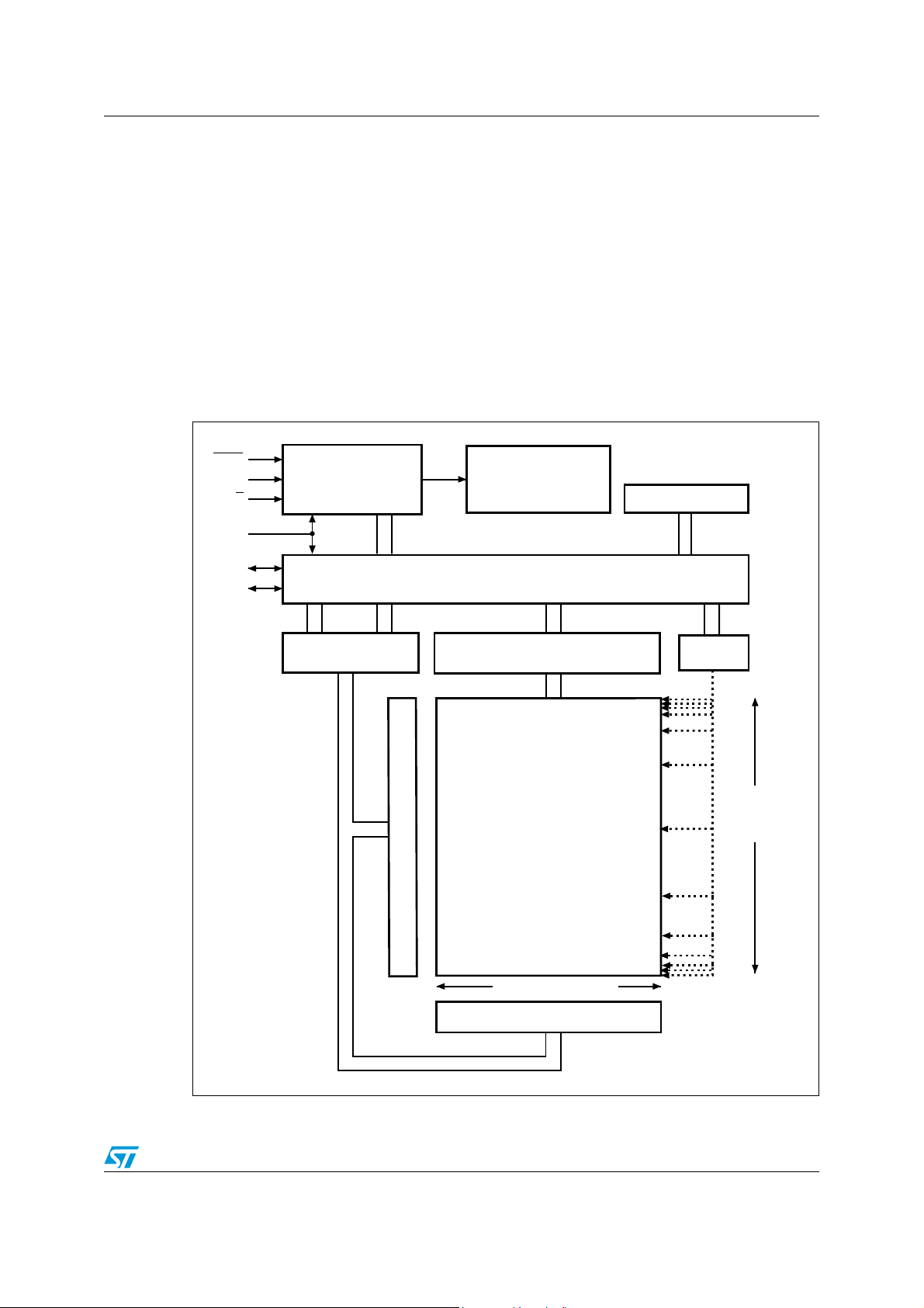
5 Memory organization
The memory is organized as:
● 4 194 304 bytes (8 bits each)
● 1024 subsectors (4 Kbytes each)
● 64 sectors (64 Kbytes each)
● 16384 pages (256 bytes each)
● 64 OTP bytes located outside the main memory array
Each page can be individually prog rammed ( bits are prog rammed from 1 t o 0). The de vice is
Subsector, Sector or Bulk Erasable (bits are erased from 0 to 1) but not Page Erasable.
Figure 7. Block diagram
HOLD
V
DQ0
DQ1
PP
Control Logic
S
C
Address Register
and Counter
Y Decoder
High Voltage
Generator
I/O Shift Register
256 Byte
Data Buffer
64 OTP bytes
Status
Register
3FFFFFh
Configurable OTP
area in main
memory array
00000h
256 Bytes (Page Size)
X Decoder
000FFh
AI13722
19/63
Page 20

Memory organization M25PX32
Table 4. Memory organization
Sector Subsector Address range Sector Subsector Address range
63
62
61
60
59
58
57
56
55
54
53
1023 3FF000h 3FFFFFh
...
...
...
52
847 34F000h 34FFFFh
...
...
...
1008 3F0000h 3F0FFFh 832 340000h 340FFFh
1007 3EF000h 3EFFFFh
...
...
...
51
831 33F000h 33FFFFh
...
...
...
992 3E0000h 3E0FFFh 816 330000h 330FFFh
991 3DF000h 3DFFFFh
...
...
...
50
815 32F000h 32FFFFh
...
...
...
976 3D0000h 3D0FFFh 800 320000h 320FFFh
975 3CF000h 3CFFFFh
...
...
...
49
799 31F000h 31FFFFh
...
...
...
960 3C0000h 3C0FFFh 784 310000h 310FFFh
959 3BF000h 3BFFFFh
...
...
...
48
783 30F000h 30FFFFh
...
...
...
944 3B0000h 3B0FFFh 768 300000h 300FFFh
943 3AF000g 3AFFFFh
...
...
...
47
767 2FF000h 2FFFFFh
...
...
...
928 3A0000h 3A0FFFh 752 2F0000h 2F0FFFh
927 39F000h 39FFFFh
...
...
...
46
751 2EF000h 2EFFFFh
...
...
...
912 390000h 390FFFh 736 2E0000h 2E0FFFh
911 38F000h 38FFFFh
...
...
...
45
735 2DF000h 2DFFFFh
...
...
...
896 380000h 380FFFh 720 2D0000h 2D0FFFh
895 37F000h 37FFFFh
...
...
...
44
719 2CF000h 2CFFFFh
...
...
...
880 370000h 370FFFh 704 2C0000h 2C0FFFh
879 36F000h 36FFFFh
...
...
...
43
703 2BF000h 2BFFFFh
...
...
...
864 360000h 360FFFh 688 2B0000h 2B0FFFh
863 35F000h 35FFFFh
...
...
...
42
687 2AF000h 2AFFFFh
...
...
...
848 350000h 350FFFh 672 2A0000h 2A0FFFh
20/63
Page 21

M25PX32 Memory organization
Table 4. Memory organization (continued)
Sector Subsector Address range Sector Subsector Address range
41
40
39
38
37
36
671 29F000h 29FFFFh
...
656 290000h 290FFFh 480 1E0000h 1E0FFFh
655 28F000h 28FFFFh
...
640 280000h 280FFFh 464 1D0000h 1D0FFFh
639 27F000h 27FFFFh
...
624 270000h 270FFFh 448 1C0000h 1C0FFFh
623 26F000h 26FFFFh
...
608 260000h 260FFFh 432 1B0000h 1B0FFFh
607 25F000h 25FFFFh
...
592 250000h 250FFFh 416 1A0000h 1A0FFFh
591 24F000h 24FFFFh
...
576 240000h 240FFFh 400 190000h 190FFFh
...
...
...
...
...
...
...
...
...
...
...
...
30
29
28
27
26
25
495 1EF000h 1EFFFFh
...
479 1DF000h 1DFFFFh
...
463 1CF000h 1CFFFFh
...
447 1BF000h 1BFFFFh
...
431 1AF000h 1AFFFFh
...
415 19F000h 19FFFFh
...
...
...
...
...
...
...
...
...
...
...
...
...
35
34
33
32
31
575 23F000h 23FFFFh
...
560 230000h 230FFFh 384 180000h 180FFFh
559 22F000h 22FFFFh
...
544 220000h 220FFFh 368 170000h 170FFFh
543 21F000h 21FFFFh
...
528 210000h 210FFFh 352 160000h 160FFFh
527 20F000h 20FFFFh
...
512 200000h 200FFFh 336 150000h 150FFFh
511 1FF000h 1FFFFFh
...
496 1F0000h 1F0FFFh 320 140000h 140FFFh
...
...
...
...
...
...
...
...
...
...
24
23
22
21
20
399 18F000h 18FFFFh
...
383 17F000h 17FFFFh
...
367 16F000h 16FFFFh
...
351 15F000h 15FFFFh
...
335 14F000h 14FFFFh
...
...
...
...
...
...
...
...
...
...
...
21/63
Page 22

Memory organization M25PX32
Table 4. Memory organization (continued)
Sector Subsector Address range Sector Subsector Address range
19
18
17
16
15
14
319 13F000h 13FFFFh
...
304 130000h 130FFFh 128 80000h 80FFFh
303 12F000h 12FFFFh
...
288 120000h 120FFFh 112 70000h 70FFFh
287 11F000h 11FFFFh
...
272 110000h 110FFFh 96 60000h 60FFFh
271 10F000h 10FFFFh
...
256 100000h 100FFFh 80 50000h 50FFFh
255 FF000h FFFFFh
...
240 F0000h F0FFFh 64 40000h 40FFFh
239 EF000h EFFFFh
...
224 E0000h E0FFFh 48 30000h 30FFFh
...
...
...
...
...
...
...
...
...
...
...
...
8
7
6
5
4
3
143 8F000h 8FFFFh
...
127 7F000h 7FFFFh
...
111 6F000h 6FFFFh
...
95 5F000h 5FFFFh
...
79 4F000h 4FFFFh
...
63 3F000h 3FFFFh
...
...
...
...
...
...
...
...
...
...
...
...
...
13
12
11
10
223 DF000h DFFFFh
...
208 D0000h D0FFFh 32 20000h 20FFFh
207 CF000h CFFFFh
...
192 C0000h C0FFFh 16 10000h 10FFFh
191 BF000h BFFFFh
...
176 B0000h B0FFFh 4 04000h 04FFFh
175 AF000h AFFFFh 3 03000h 03FFFh
160 A0000h A0FFFh 1 01000h 01FFFh
159 9F000h 9FFFFh 0 00000h 00FFFh
9
...
144 90000h 90FFFh
...
...
...
...
...
...
...
...
2
1
0
47 2F000h 2FFFFh
...
31 1F000h 1FFFFh
...
15 0F000h 0FFFFh
...
2 02000h 02FFFh
...
...
...
...
...
...
22/63
Page 23

M25PX32 Instructions
6 Instructions
All instructions, addresses and data are shifted in and ou t of the device, most significant bit
first.
Serial Data input(s) DQ0 (DQ1) is (are) sampled on the first rising edge of Serial Cloc k (C)
after Chip Select (S
the device, most significant bit first, on Serial Data input(s) DQ0 (DQ1), each bit being
latched on the rising edges of Serial Clock (C).
The instruction set is listed in Table 5.
Every instruction sequence starts with a one-byte instruction code. Depending on the
instruction, this might be followed by address bytes, or by data bytes, or by both or none.
In the case of a Read Data Bytes (READ), Read Data Bytes at higher speed (Fast_Read),
Dual Output Fast Read (DOFR), Read OTP (ROTP), Read Lock Registers (RDLR), Read
Status Register (RDSR), Read Identification (RDID) or Release from Deep Power-do wn
(RDP) instruction, the shifted-in instruction sequence is followed by a data-out sequence.
Chip Select (S
out.
In the case of a Page Program (PP), Program OTP (POTP), Dual Input Fast Program
(DIFP), Subsector Erase (SSE), Sector Erase (SE), Bulk Erase (BE), Write Status Register
(WRSR), Write to Lock Register (WRLR), Write Enable (WREN), Write Disable (WRDI) or
Deep Power-down (DP) instruction, Chip Select (S
boundary, otherwise the instruction is rejected, and is not executed. That is, Chip Sele ct (S
must driven High when the number of clock pulses after Chip Select (S
an exact multiple of eight.
) is driven Low. Then, the one-byte instruction code m ust be shifted in to
) can be driven High after any bit of the data-out sequence is being shifted
) must be driven High exactly at a byte
) being driven Low is
)
All attempts to access the memory array during a Write Status Register cycle, Program
cycle or Erase cycle are ignored, and the internal Write Status Register cycle, Program
cycle or Erase cycle continues unaffected.
23/63
Page 24

Instructions M25PX32
Table 5. Instruction set
Instruction Description
One-byte instruction
code
Address
bytes
Dummy
bytes
WREN Write Enable 0000 0110 06h 0 0 0
WRDI Write Disable 0000 0100 04h 0 0 0
1001 1111 9Fh 0 0 1 to 20
RDID Read Identification
1001 1110 9Eh 0 0 1 to 3
RDSR Read Status Register 0000 0101 05h 0 0 1 to ∞
WRSR Write Status Register 0000 0001 01h 0 0 1
WRLR Write to Lock Register 1110 0101 E5h 3 0 1
RDLR Read Lock Register 1110 1000 E8h 3 0 1
READ Read Data Bytes 0000 0011 03h 3 0 1 to ∞
FAST_READ
Read Data Bytes at higher
speed
0000 1011 0Bh 3 1 1 to ∞
DOFR Dual Output Fast Read 0011 1011 3Bh 3 1 1 to ∞
ROTP
POTP
Read OTP (Read 64 bytes of
OTP area)
Program OTP (Program 64
bytes of OTP area)
0100 1011 4Bh 3 1 1 to 65
0100 0010 42h 3 0 1 to 65
PP Page Program 0000 0010 02h 3 0 1 to 256
DIFP Dual Input Fast Program 1010 0010 A2h 3 0 1 to 256
SSE Subsector Erase 0010 0000 20h 3 0 0
Data
bytes
SE Sector Erase 1101 1000 D8h 3 0 0
BE Bulk Erase 1100 0111 C7h 0 0 0
DP Deep Power-down 1011 1001 B9h 0 0 0
RDP
Release from Deep Powerdown
1010 1011 ABh 0 0 0
24/63
Page 25

M25PX32 Instructions
6.1 Write Enable (WREN)
The Write Enable (WREN) instruction (Figure 8) sets the Write Enable Latch (WEL) bit.
The Write Enable Latch (WEL) bit must be set prior to e very Page Program (PP), Dual Input
Fast Prog ram (DIFP), Program OTP (POTP), Write to Lock Register (WRLR), Subsector
Erase (SSE), Sector Erase (SE), Bulk Erase (BE) and Write Status Register (WRSR)
instruction.
The Write Enable (WREN) instruction is entered by driving Chip Select (S
instruction code, and then driving Chip Select (S
) High.
Figure 8. Write Enable (WREN) instruction sequence
S
0
21 34567
C
Instruction
DQ0
High Impedance
DQ1
AI13731
) Low , send ing the
25/63
Page 26

Instructions M25PX32
6.2 Write Disable (WRDI)
The Write Disable (WRDI) instruction (Figure 9) resets the Write Enable Latch (WEL) bit.
The Write Disable (WRDI) instruction is entered by driving Chip Select (S
instruction code, and then driving Chip Select (S
) High.
The Write Enable Latch (WEL) bit is reset under the following conditions:
● Power-up
● Write Disable (WRDI) instruction completion
● Write Status Register (WRSR) instruction completion
● Write lo Lock Register (WRLR) instruction completion
● P age Program (PP) instruction completion
● Dual Input Fast Program (DIFP) instruction completion
● Program OTP (POTP) instruction completion
● Subsector Erase (SSE) instruction completion
● Sector Erase (SE) instruction completion
● Bulk Erase (BE) instruction completion
Figure 9. Write Disable (WRDI) instruction sequence
S
0
21 34567
C
Instruction
) Low , se nding the
DQ0
DQ1
High Impedance
AI13732
26/63
Page 27

M25PX32 Instructions
6.3 Read Identification (RDID)
The Read Identification (RDID) instruction allows to read the device identification data:
● Manufacturer identification (one byte)
● Device identification (two bytes)
● A Unique ID code (UID) followed by 16 bytes of CFI data
The manufacturer identification is assigned by JEDEC, and has the value 20h for
STMicroelectronics. The device identification is assigned by the device manufacturer, and
indicates the memory type in the first byte (71h), and the memory capacity of the device in
the second byte (16h). The UID is set to 10h and indicates that 16 bytes, related to the CFI
content, are following.
Any Read Identification (RDID) instruction while an Erase or Progr am cycle is in progress, is
not decoded, and has no effect on the cycle that is in progress.
The Read Identification (RDID) instruction should not be issued while the device is in Deep
Pow er-down mode.
The device is first selected by driving Chip Select (S
) Low. Then, the 8-bit instruction code
for the instruction is shifted in. After this, the 24-bit device identification, stored in the
memory, the 8-bit Unique ID code followed by 16 bytes of CFI content will be shifted out on
Serial Data output (DQ1). Each bit is shifted out during the falling edge of Serial Clock (C).
The instruction sequence is shown in Figure 10.
The Read Identification (RDID) instruction is terminated by driving Chip Select (S
any time during data output.
When Chip Select (S
) is driven High, the de vice is put in the Standby Power mode. Once in
the Standby P o wer m ode, the de vice w aits to be selected , so that it can receiv e, decode and
execute instructions.
Table 6. Read Identification (RDID) data-out sequence
Manufacturer identification
Device identification
UID CFI content
Memory type Memory capacity
20h 71h 16h 10h 16 bytes
Figure 10. Read Identification (RDID) instruction sequence and data-out sequence
S
0
213456789101112131415
C
Instruction
DQ0
16 17 18 28 29 30 31
) High at
DQ1
High Impedance
Manufacturer Identification
MSB
Device Identification
15
14 13 3 2 1 0
MSB
UID + CFI Data
MSB
AI06809d
27/63
Page 28

Instructions M25PX32
6.4 Read Status Register (RDSR)
The Read Status Register (RDSR) instruction allows the Status Register to be read. The
Status Register may be read at any time, even while a Program, Erase or Write Status
Register cycle is in progress. When one of these cycles is in progress, it is recommended to
check the Write In Progress (WIP) bit before sending a new instruction to the device. It is
also possible to read the Status Register continuously, as shown in Figure 11.
Table 7. Status Register format
b7 b0
SRWD 0 TB BP2 BP1 BP0 WEL WIP
Status Register Write Protect
Top/Bottom bit
Block Protect bits
Write Enable Latch bit
Write In Progress bit
The status and control bits of the Status Register are as follows:
6.4.1 WIP bit
The Write In Progress (WIP) bit indicates whether the memory is busy with a Write Status
Register, Program or Erase cycle. When set to 1, such a cycle is in progress, when reset to
0 no such cycle is in progress.
6.4.2 WEL bit
The Write Enable Latch (WEL) bit indicates the status of the internal Write Enable Latch.
When set to 1 the internal Write Enable Latch is set, when set to 0 the internal Write Enable
Latch is reset and no Write Status Register, Program or Erase instruction is accepted.
6.4.3 BP2 , BP1, BP0 bits
The Block Protect (BP2, BP1, BP0) bits are non-volatile. They define the size of the area to
be software protected against Program and Erase instructions. These bits are written with
the Write Status Register (WRSR) instruction. When one or more of the Block Protect (BP2,
BP1, BP0) bits is set to 1, the relevant memory area (as defined in Table 3) becomes
protected against Page Program (PP) and Sector Erase (SE) instructions. The Block Protect
(BP2, BP1, BP0) bits can be written provided that the Hardware Protected mode has not
been set. The Bulk Erase (BE) instruction is executed if, and only if, all Block Protect (BP2,
BP1, BP0) bits are 0.
28/63
Page 29

M25PX32 Instructions
6.4.4 TB bit
The Top/Bottom (TB) bit is non-volatile. It can be set and reset with the Write Status
Register (WRSR) instruction provided that the Write Enable (WREN) instruction has been
issued. The Top/Bottom (TB) bit is used in conjunction with the Block Protect (BP0, BP1,
BP2) bits to determine if the protected area defined by the Block Protect bits starts from the
top or the bottom of the memory array:
● When TB is reset to ‘0’ (default value), the area protected by the Block Protect bits
starts from the to p of th e me m ory array (see Table 3: Protected area sizes)
● When TB is set to ‘1’, the area prote cted by the Block Protect bits starts from the
bottom of the memory array (see Table 3: Protected area sizes)
The TB bit cannot be written when the SRWD bit is set to ‘1’ and t he W
6.4.5 SRWD bit
The Status Register Write Disable (SRWD) bit is operated in conjunction with the Write
Protect (W
(W
/VPP) signal allow the device to be put in the hardware protected mode (when the Status
Register Write Disable (SRWD) bit is set to ‘1’, and Write Protect (W
this mode, the non-volatile bits of the Status Register (SRWD, BP2, BP1, BP0) become
read-only bits and the Write Status Register (WRSR) instruction is no longer accepted for
execution.
Figure 11. Read Status Register (RDSR) instruction sequence and data-out
S
C
DQ0
DQ1
pin is driven Low.
/VPP) signal. The Status Register Write Disable (SRWD) bit and the Write Protect
/VPP) is driven Low). In
sequence
21 3456789101112131415
0
Instruction
High Impedance
Status Register Out
7 6543210
MSB
Status Register Out
7 6543210
MSB
7
AI13734
29/63
Page 30

Instructions M25PX32
6.5 Write Status Register (WRSR)
The Write Status Register (WRSR) instruction allows new values to be written to the Status
Register. Before it can be accepted, a Write Enable (WREN) instruction must previously
have been executed. After the Write Enable (WREN) instruction has been decoded and
executed, the device sets the Write Enable Latch (WEL).
The Write Status Register (WRSR) instruction is entered by driving Chip Select (S
) Low,
followed by the instruction code and the data byte on Serial Data inpu t (DQ0).
The instruction sequence is shown in Figure 12.
The Write Status Register (WRSR) instruction has no effect on b6, b1 and b0 of the Status
Register. b6 is always read as ‘0’.
Chip Select (S
) must be driven High after t he eighth bit of th e data b y te has bee n latched in .
If not, the Write Status Register (WRSR) instruction is not executed. As soon as Chip Select
(S
) is driven High, the self-timed Write Status Register cycle (whose duration is tW) is
initiated. While the Write Status Register cycle is in progress, the Status Register may still
be read to check the value of the Write In Progress (WIP) bit. The Write In Progress (WIP)
bit is 1 during the self-timed Write Status Register cycle, and is 0 when it is completed.
When the cycle is completed, the Write Enable Latch (WEL) is r eset.
The Write Status Register (WRSR) instruction allows the user to change the values of the
Block Protect (BP2, BP1, BP0) bits, to define the size of the area that is to be treated as
read-only, as defined in Table 3. The Write Status Register (WRSR) instruction also allows
the user to set and reset the Status Register Write Disable (SRWD) bit in accordance with
the Write Protect (W
Protect (W
/VPP) signal allow the device to be put in the hardware protected mode (HPM).
/VPP) signal. The Status Register Write Disable (SRWD) bit and Write
The Write Status Register (WRSR) instruction is not e xecuted once the hardware protected
mode (HPM) is entered.
Figure 12. Write Status Register (WRSR) instruction sequence
S
21 3456789101112131415
0
C
Instruction Status
DQ0
High Impedance
DQ1
30/63
Register In
765432 0
MSB
1
AI13735
Page 31

M25PX32 Instructions
Table 8. Protection modes
W/VPP
signal
10
00
11
01
1. As defined by the values in the Block Protect (BP2, BP1, BP0) bits of the Status Register, as shown in
Table 3.
SRWD
bit
Mode
Software
protected
(SPM)
Hardware
protected
(HPM)
Write Protection
of the Status
Register
Status Register is
Writable (if the
WREN instruction
has set the WEL
bit)
The values in the
SRWD, BP2, BP1
and BP0 bits can
be changed
Status Register is
hardware write
protected
The values in the
SRWD, BP2, BP1
and BP0 bits
cannot be changed
Protected area
Protected against
Page Program,
Sector Erase and
Bulk Erase
Protected against
Page Program,
Sector Erase and
Bulk Erase
Memory content
(1)
Unprotected area
Ready to accept
Page Program and
Sector Erase
instructions
Ready to accept
Page Program and
Sector Erase
instructions
(1)
The protection features of the device are summarized in Table 8.
When the Status Register Write Disable (SRWD) bit of the Status Register is 0 (its initial
delivery state), it is possible to write to the Status Register provid ed that the Write Enable
Latch (WEL) bit has previously been set by a Write Enable (WREN) instruction, regardless
of the whether Write Protect (W
/VPP) is driven High or Low.
When the Status Register Write Disable (SRWD) bit of the Status Register is set to 1, two
cases need to be considered, depending on the state of Write Protect (W
● If Write Protect (W/V
) is driven High, it is possible to write to the Status Register
PP
/VPP):
provided that the Write Enable Latch (WEL) bit has previously been set by a Write
Enable (WREN) instruction.
● If Write Protect (W/V
) is driven Low, it is not possible to write to the Status Register
PP
even if the Write Enable Latch (WEL) bit has previously been set by a Write Enable
(WREN) instruction. (Attempts to write to the Status Register are rejected, and are not
accepted for execution). As a consequence, all the data bytes in the memory area that
are software protected (SPM) by the Block Protect (BP2, BP1, BP0) bits of the Status
Register, are also hardware protected against data modification.
Regardless of the order of the two events, the Hardware Protected mode (HPM) can be
entered:
● by setting the Status Register Write Disable (SRWD) bit after driving Write Protect
(W
/VPP) Low
● or by driving Write Protect (W/V
) Low after setting the Status Register Write Disable
PP
(SRWD) bit.
The only way to exit the Hardware Protected mode (HPM) once entered is to pull Write
Protect (W
If Write Protect (W
/VPP) High.
/VPP) is permanently tied High, the Hardware Protected mode (HPM) can
never be activated, and only the Software Protected mode (SPM), using the Block Protect
(BP2, BP1, BP0) bits of the Status Register, can be used.
31/63
Page 32

Instructions M25PX32
6.6 Read Data Bytes (READ)
The device is first selected by driving Chip Select (S) Low. The instruction code for the Read
Data Bytes (READ) instruction is followed by a 3-byte address (A23-A0), each bit being
latched-in during the rising edge of Serial Clock (C). Then the memory contents, at that
address, is shifted out on Serial Data output (DQ1), each bit being shifted out, at a
maximum frequency f
The instruction sequence is shown in Figure 13.
The first byte addressed can be at any location. The address is automatically incremented
to the next higher address after each byte of data is shifted out. The whole memory can,
therefore, be read with a single Read Data Bytes (READ) instruction. When the highest
address is reached, the address counter rolls over to 000000h, allowing the read sequence
to be continued indefinitely.
, during the falling edge of Serial Clock (C).
R
The Read Data Bytes (READ) instruction is terminated by driving Chip Select (S
Select (S
) can be driven High at any time during data output. Any Read Data Bytes (READ)
) High. Chip
instruction, while an Erase, Program or Write cycle is in progress, is rejected without having
any effects on the cycle that is in progress.
Figure 13. Read Data Bytes (READ) instruction sequence and data-out sequence
S
21 345678910 2829303132333435
0
C
Instruction 24-bit address
DQ0
DQ1
1. Address bits A23 to A22 are Don’t care.
High Impedance
23
2221 3210
MSB
76543 1 7
MSB
36 37 38
Data Out 1
39
Data Out 2
2
0
AI13736
32/63
Page 33

M25PX32 Instructions
6.7 Read Data Bytes at higher speed (FAST_READ)
The device is first selected by driving Chip Select (S) Low. The instruction code for the Read
Data Bytes at higher speed (FAST_READ) instruction is followed by a 3-b yte address (A23A0) and a dummy byte, each bit being latched-in during the rising edge of Serial Clock (C).
Then the memory contents, at that address , are shif ted out o n Serial Data output (D Q1) at a
maximum frequency f
The instruction sequence is shown in Figure 14.
The first byte addressed can be at any location. The address is automatically incremented
to the next higher address after each byte of data is shifted out. The whole memory can,
therefore, be r ead with a single Read Data Bytes at higher speed (FAST_READ) instruction.
When the highest address is reached, the address counter rolls over to 000000h, allo wing
the read sequence to be continued indefinite ly.
The Read Data Bytes at higher speed (FAST_READ) instruction is terminated by driving
Chip Select (S
) High. Chip Select (S) can be driven High at any time du ring data output. An y
Read Data Bytes at higher speed (FAST_READ) instruction, while an Erase, Program or
Write cycle is in progress, is rejected without having any effects on the cycle that is in
progress.
Figure 14. Read Data Bytes at higher speed (FAST_READ) instruction sequence
and data-out sequence
, during the falling edge of Serial Clock (C).
C
DQ0
DQ1
S
C
DQ0
DQ1
21 345678910 28293031
0
Instruction 24-bit address
23
2221 3210
High Impedance
S
32 33 34 36 37 38 39 40 41 42 43 44 45 46
C
765432 0
35
Dummy byte
1
DATA OUT 1
765432 0
MSB
47
DATA OUT 2
7 6543210
1
MSB MSB
7
1. Address bits A23 to A22 are Don’t care.
AI13737
33/63
Page 34

Instructions M25PX32
6.8 Dual Output Fast Read (DOFR)
The Dual Output Fast Read (DOFR) instruction is very similar to the Read Data Bytes at
higher speed (FAST_READ) instruction, except that the data are shifted out on two pins (pin
DQ0 and pin DQ1) instead of only one. Outputting the data on two pins instead of one
doubles the data transfer bandwidth compared to the Read Data Bytes at higher speed
(FAST_READ) instruction.
The device is first selected by driving Chip Select (S
) Low . The instruction code for the Dual
Output Fast Read instruction is followed b y a 3-byte address (A23-A0) and a dummy byte,
each bit being latched-in during the rising edge of Serial Clock (C). Then the memory
contents, at that address, are shifted out on DQ0 and DQ1 at a maximum frequency f
,
C
during the falling edge of Serial Clock (C).
The instruction sequence is shown in Figure 15.
The first byte addressed can be at any location. The address is automatically incremented
to the next higher address after each byte of data is shifted ou t on DQ0 and DQ1. The whole
memory can, therefore, be read with a single Dual Output Fast Read (DOFR) instruction.
When the highest address is reached, the address counter rolls over to 00 0000h, so that
the read sequence can be continued indefinitely.
Figure 15. Dual Output Fast Read instruction sequence
S
DQ0
DQ1
C
Mode 3
Mode 2
21 345678910 282930310
Instruction 24-bit address
23 22 21 3 2 1 0
High Impedance
S
32 33 34 36 37 38 39 40 41 42 43 44 45 46
C
DQ0
DQ1
1. A23 to A22 are Don't care.
35
Dummy byte
642064 02
DATA OUT 1
753175 1
MSB
34/63
47
6420 64 02
DATA OUT 2 DATA OUT 3 DATA OUT n
7 531 7531
3
MSB MSB
MSB MSB
ai13574
Page 35

M25PX32 Instructions
6.9 Read Lock Register (RDLR)
The device is first selected by driving Chip Select (S) Low. The instruction code for the Read
Lock Register (RDLR) instruction is followed by a 3-byte address (A23-A0) pointing to any
location inside the concerned sector. Each ad dress bit is latched-in during the rising edge of
Serial Clock (C). Then the value of the Lock Register is shifted out on Serial Data outp u t
(DQ1), each bit being shifted out, at a maximum frequency f
Serial Clock (C).
The instruction sequence is shown in Figure 16.
, during the falling edge of
C
The Read Lock Register (RDLR) instruction is terminated by driving Chip Select (S
) High at
any time during data output.
Any Read Lock Register (RDLR) instruction, while an Erase, Program or Write cycle is in
progress, is rejected without having any effects on the cycle that is in progress.
Table 9. Lock Register out
Bit Bit name Value Function
b7-b2 Reserved
b1 Sector Lock Down
b0 Sector Write Lock
1. Values of (b1, b0) after Power-up are defined in Section 7: Power-up and power-down.
(1)
The Write Lock and Lock Down bits cannot be changed.
‘1’
Once a ‘1’ is written to the Lock Down bit it cannot be cleared
to ‘0’, except by a power-up.
The Write Lock and Lock Down bits can be changed by
‘0’
writing new values to them.
Write, Program and Erase operations in this sector will not be
‘1’
executed. The memory contents will not be changed.
Write, Program and Erase operations in this sector are
‘0’
executed and will modify the sector contents.
Figure 16. Read Lock Register (RDLR) instruction sequence and data-out sequence
S
DQ0
DQ1
21 345678910 2829303132333435
0
C
Instruction 24-bit address
23
2221 3210
MSB
High Impedance
Lock Register Out
76543 1
MSB
36 37 38
2
39
0
AI13738
35/63
Page 36

Instructions M25PX32
6.10 Read OTP (ROTP)
The device is first selected by driving Chip Select (S) Low. The instruction code for the Read
OTP (ROTP) instruction is f o llowed by a 3-byte ad dress (A23 - A0 ) and a dum my byte. Each
bit is latched in on the rising edge of Serial Clock (C).
Then the memory conte nt s at th at ad d re ss ar e sh ifte d ou t on Serial Data output (DQ1).
Each bit is shifted out at the maximum frequency, f
(C). The instruction sequence is shown in Figure 17.
The address is automatically incremented to the next higher address after each b yte of data
is shifted out.
There is no rollover mechanism with the Re ad OTP (ROT P) instruction. This means that the
Read OTP (ROTP) instruction must be sent with a maximum of 65 b ytes to read , since once
th
the 65
byte has been read, the same (65th) byte keeps being read on the DQ1 pin.
max, on the falling edg e of Serial Clock
C
The Read OTP (RO TP) instruction is terminated by driving Chip Select (S
(S
) can be driven High at any time during data output. Any Read OTP (ROTP) instruction
) High. Chip Select
issued while an Erase, Program or Write cycle is in progress, is rejected without having any
effect on the cycle that is in progress.
Figure 17. Read OTP (ROTP) instruction and data-out sequence
S
21 345678910 28293031
0
C
Instruction 24-bit address
23
DQ0
DQ1
High Impedance
S
32 33 34 36 37 38 39 40 41 42 43 44 45 46
C
35
2221 3210
47
Dummy byte
DQ0
DQ1
1. A23 to A7 are Don't care.
2. 1 ≤ n ≤ 65.
765432 0
1
765432 0
MSB
36/63
DATA OUT 1
DATA OUT n
1
7 6543210
MSB MSB
7
AI13573
Page 37

M25PX32 Instructions
6.11 Page Program (PP)
The Page Program (PP) instruction allows bytes to be progra mmed in the memory
(changing bits from 1 to 0). Before it can be accepted, a Write Enable (WREN) instruction
must previously have been executed. After the Write Enable (WREN) instruction has been
decoded, the device sets the Write Enable Latch (WEL).
The Page Program (PP) instruction is entered by driving Chip Select (S
the instruction code, three address bytes and at least one data byte on Serial Data input
(DQ0). If the 8 least significant address bits (A7-A0) are not all z ero , all tr ansmitted data that
goes beyond the end of the current page are programmed f rom the start address of the
same page (from the address whose 8 least significant bits (A7-A0) are all zero). Chip
Select (S
The instruction sequence is shown in Figure 18.
If more than 256 by tes ar e se nt t o the device, previo usly latche d data are discarded and the
last 256 data bytes are guaranteed t o be progr ammed correctly within the same page . If less
than 256 data bytes are sent to device, they are correctly programmed at the requested
addresses without having any effects on the other bytes of the same page.
For optimized timings, it is recommended to use the Page Program (PP) instruction to
program all consecutive targeted bytes in a single sequence versus using several Page
Program (PP) sequences with each containing only a few bytes (see Table 17: AC
characteristics).
Chip Select (S
latched in, otherwise the Page Program (PP) instruction is not ex ecuted.
As soon as Chip Select (S
duration is t
may be read to check the value of the Write In Progress (WIP) bit. The Write In Progress
(WIP) bit is 1 during the self-timed Page Program cycle, and is 0 when it is completed. At
some unspecified time before the cycle is completed, the Write Enable Latch (WEL) bit is
reset.
) must be driven Low for the entire duration of the sequence.
) must be driven High after the eighth bit of the last data byte has been
) is driven High, the self-timed Page Program cycle (whose
) is initiated. While the Page Program cycle is in progress , the Statu s Register
PP
) Low, followed by
A Page Progr am (PP) instruction applied to a page which is protected by the Block Protect
(BP2, BP1, BP0) bits (see Table 3 and Table 4) is not executed.
37/63
Page 38

Instructions M25PX32
Figure 18. Page Program (PP) instruction sequence
S
21 345678910 2829303132333435
0
C
Instruction 24-bit address
DQ0
S
4241 43 44 45 46 47 48 49 50 52 53 54 5540
C
Data byte 2
DQ0
765432 0
MSB MSB MSB
1
1. Address bits A23 to A22 are Don’t care.
23
2221 3210
MSB
51
Data byte 3 Data byte 256
765432 0
1
765432 0
MSB
2072
765432 0
Data byte 1
2074
2073
36 37 38
2076
2075
2077
1
1
2078
39
2079
AI13739
38/63
Page 39

M25PX32 Instructions
6.12 Dual Input Fast Program (DIFP)
The Dual Input Fast Program (DIFP) instruction is very similar to the Page Program (PP)
instruction, except that the data are entered on two pins (pin DQ0 and pin DQ1) instead of
only one. Inputting the data on two pins instead of one doubles the data transfer bandwidth
compared to the Pag e Program (PP) instruction.
The Dual Input Fast Program (DIFP) instruction is entered by driving Chip Select (S
followed by the instruction code, three address bytes and at least one data byte on Serial
Data input (DQ0).
If the 8 least significant address bits (A7-A0) are not all zero, all transmitted data that goes
beyond the end of t he current page are programmed from the start address of the same
page (from the address whose 8 least significant bits (A7-A0) are all zero). Chip Select (S
must be driven Low for the entire duration of the sequence.
The instruction sequence is shown in Figure 19.
If more than 256 by tes ar e se nt t o the device, previo usly latche d data are discarded and the
last 256 data bytes are guaranteed t o be progr ammed correctly within the same page . If less
than 256 data bytes are sent to device, they are correctly programmed at the requested
addresses without having any effects on the other bytes in the same page.
For optimized timings, it is recommended to use the Dual Input Fast Program (DIFP)
instruction to program all consecutive targeted bytes in a single sequence rather to using
several Dual Input Fast Program (DIFP) sequences each containing only a few bytes (see
Table 17: AC characteristics).
Chip Select (S
latched in, otherwise the Dual Input Fast Program (DIFP) instruction is not executed.
As soon as Chip Select (S
duration is t
the Status Register may be read to check the value of the Write In Progress (WIP) bit. The
Write In Progress (WIP) bit is 1 during the self-timed Page Program cycle, and 0 when it is
completed. At some unspecified time before the cycle is completed, the Write Enable Latch
(WEL) bit is reset.
) must be driven High after the eighth bit of the last data byte has been
) is driven High, the self-timed Page Program cycle (whose
) is initiated. While the Dual Input Fast Program (DIFP) cycle is in progress,
PP
) Low,
)
A Dual Input Fast Program (DIFP) instruction applied to a page that is protected by the
Block Protect (BP2, BP1, BP0) bits (see Table 2 and Table 3) is not executed.
39/63
Page 40

Instructions M25PX32
Figure 19. Dual Input Fast Program (DIFP) instruction sequence
S
21 345678910 28293031
0
C
Instruction 24-bit address
23
DQ0
2221 3210
DQ1
S
3433 35 36 37 38 39 40 41 42 44 45 46 4732 43
C
DQ0
DQ1
642064 02642064 0
DATA IN 1 DATA IN 4 DATA IN 5 DATA IN 256DATA IN 3DATA IN 2
7531
MSB MSB
1. A23 to A22 are Don't care.
High Impedance
1753
7
5
MSB
2
753
31 1
MSB
6420
7531
MSB
6420
7531
MSB
AI14229
40/63
Page 41

M25PX32 Instructions
6.13 Program OTP instruction (POTP)
The Program OTP instruction (POTP) is used to program at most 64 bytes to the OTP
memory area (by changing bits from 1 to 0, only). Before it can be accepted, a Write Enable
(WREN) instruction must previously have been ex ecuted. After the Write Enable (WREN)
instruction has been decoded, the device sets the Write Enable Latch (WEL) bit.
The Program OTP instruction is entered by driving Chip Select (S
) Low, followed by the
instruction opcode, three address bytes and at least one data byte on Serial Data input
(DQ0).
Chip Select (S
) must be driven High after the eighth bit of the last data byte has been
latched in, otherwise the Program OTP instruction is not executed.
There is no rollover mechanism with the Program OTP (POTP) instruction. This means that
the Program OTP (POTP) instruction must be sent wit h a maxim u m of 65 bytes to program,
once all 65 bytes have been latched in, any following byte will be discarded.
The instruction sequence is shown in Figure 20.
As soon as Chip Select (S
duration is t
) is initiated. While the Program OTP cycle is in progress, the Status Register
PP
) is driven High, the self-timed Page Program cycle (whose
may be read to check the value of the Write In Progress (WIP) bit. The Write In Progress
(WIP) bit is 1 during the self-timed Program OTP cycle, and it is 0 when it is completed. At
some unspecified time before the cycle is complete, the Write Enable Latch (WEL) bit is
reset.
To lock the OTP memory:
Bit 0 of the OTP cont rol b yte, that is b yte 64, (see Figure 21) is used to permanently lock the
OTP memory array.
● When bit 0 of b yte 64 = ’1’, the 64 b y tes of t he OTP memory array can be progr a mmed.
● When bit 0 of byte 64 = ‘0’, the 64 bytes of the OTP memor y ar ray are read-only and
cannot be programmed anymore.
Once a bit of the OTP memory has been progr ammed to ‘0’, it can no longer be set to ‘1’.
Therefore, as soon as bit 0 of byte 64 (control byte) is set to ‘0’, the 64 bytes of the OTP
memory array become read-only in a permanent way.
Any Program OTP (POTP) instruction issued while an Erase, Program or Write cycle is in
progress is rejected without having any effect on the cycle that is in progress.
41/63
Page 42

Instructions M25PX32
Figure 20. Program OTP (POTP) instruction sequence
S
21 345678910 2829303132333435
0
C
Instruction 24-bit address
23
DQ0
S
C
DQ0
4241 43 44 45 46 47 48 49 50 52 53 54 5540
Data byte 2
765432 0
MSB MSB MSB
1
2221 3210
MSB
51
Data byte 3 Data byte n
765432 0
1
1. A23 to A7 are Don't care.
2. 1 ≤ n ≤ 65
Figure 21. How to permanently lock the 64 OTP bytes
36 37 38
Data byte 1
765432 0
MSB
765432 0
1
1
39
AI13575
Byte0Byte1Byte
2
X X X X X X X bit 0
Bit 1 to bit 7 are NOT
programmable
OTP Control byte64 data bytes
Byte
Byte
64
63
When bit 0 = 0
the 64 OTP bytes
become READ only
ai13587
42/63
Page 43

M25PX32 Instructions
6.14 Write to Lock Register (WRLR)
The Write to Lock Register (WRLR) instruction allows bits to be changed in the Lock
Registers. Bef ore it can be accepted, a Write Enable (WREN) instruction must previously
have been executed. After the Write Enable (WREN) instruction has been decoded, the
device sets the Write Enable Latch (WEL).
The Write to Lock Register (WRLR) instruction is entered by driving Chip Select (S
) Low,
followed b y the instruction code , three address b ytes (pointing to an y address in the targeted
sector and one data byte on Serial Data input (DQ0). The instruction sequence is shown in
Figure 22. Chip Select (S
) must be driven High after the eighth bit of the data b yte has b een
latched in, otherwise the Write to Lock Register (WRLR) instruction is not executed.
Lock Register bits are volatile, and therefore do not require time to be written. When the
Write to Lock Register (WRLR) instruction has been successfully executed, the Write
Enable Latch (WEL) bit is reset after a delay time less than t
minimum value.
SHSL
Any Write to Lock Register (WRLR) instruction, while an Erase, Program or Write cycle is in
progress, is rejected without having any effects on the cycle that is in progress.
Figure 22. Write to Lock Register (WRLR) instruction sequence
S
21 345678910 2829303132333435
C
DQ0
0
Instruction 24-Bit Address
23
MSB
2221 3210
765432 0
MSB
36 37 38
Lock Register
In
39
1
AI13740
Table 10. Lock Register in
(1)
Sector Bit Value
b7-b2 ‘0’
All sectors
b1 Sector Lock Down bit value (refer to Table 9)
b0 Sector Write Lock bit value (refer to Table 9)
1. Values of (b1, b0) after Power-up are defined in Section 7: Power-up and power-down.
43/63
Page 44

Instructions M25PX32
6.15 Subsector Erase (SSE)
The Subsector Erase (SSE) instruction sets to 1 (FFh) all bits inside the chosen subsector.
Before it can be accepted, a Write Enable (WREN) instruction must previously have been
exe cuted. After the Write Enable (WREN) instruction has been decoded, the de vice sets the
Write Enable Latch (WEL).
The Subsector Erase (SSE) instruction is entered by driving Chip Select (S
) Low, followed
by the instruction code, and three address bytes on Serial Data input (DQ0). Any address
inside the Subsector (see Table 4) is a valid address for the Subsector Erase (SSE)
instruction. Chip Select (S
) must be driven Low for the entire duration of the sequence.
The instruction sequence is shown in Figure 23.
Chip Select (S
) must be driven High after the eighth bit of the last address byte has been
latched in, otherwise the Subsector Erase (SSE) instruction is not executed. As soon as
Chip Select (S
) is driven High, the self-timed Subsector Erase cycle (whose dur ation is t
SSE
is initiated. While the Subsector Erase cycle is in progress, the Status Register may be read
to check the valu e of the Write In Progress (WIP) bit. The Write In Progress (WIP) bit is 1
during the self-timed Subsector Erase cycle, and is 0 when it is completed. At some
unspecified time before the cycle is comple te, the Write Enable Latch (WEL) bit is reset.
A Subsector Erase (SSE) instruction issued to a sector that is hardware or software
protected, is not executed.
Any Subsector Erase (SSE) instruction, while an Erase, Program or Write cycle is in
progress, is rejected without having any effects on the cycle that is in progress.
Figure 23. Subsector Erase (SSE) instruction sequence
S
21 3456789 293031
0
C
)
Instruction
DQ0
1. Address bits A23 to A22 are Don’t care.
44/63
23 22
MSB
24 Bit Address
20
1
AI13741
Page 45

M25PX32 Instructions
6.16 Sector Erase (SE)
The Sector Erase (SE) instruction sets to 1 (FFh) all bits inside the chosen sector. Before it
can be accepted, a Write Enable (WREN) instruction must previously have been executed.
After the Write Enable (WREN) instruction has been decoded, the device sets the Write
Enable Latch (WEL).
The Sector Erase (SE) instruction is entered by driving Chip Select (S
) Low, followed by the
instruction code, and three address bytes on Serial Data input (DQ0). Any address inside
the Sector (see Table 4) is a valid address for the Sector Erase (SE) instruction. Chip Select
(S
) must be driven Low for the entire duration of the sequence.
The instruction sequence is shown in Figure 24.
Chip Select (S
) must be driven High after the eighth bit of the last address byte has been
latched in, otherwise the Sector Erase (SE) instruction is not executed. As soon as Chip
Select (S
) is driven High, the self-timed Sector Erase cycle (whose duration is tSE) is
initiated. While the Sector Erase cycle is in progress, the Status Register may be read to
check the value of the Write In Progress (WIP) bit. The Write In Progress (WIP) bit is 1
during the self-timed Sector Erase cycle, and is 0 when it is completed. At some unspecified
time before the cycle is completed, the Write Enable Latch (WEL) bit is reset.
A Sector Erase (SE) instruction applied to a page which is protected by the Block Protect
(BP2, BP1, BP0) bits (see Table 3 and Table 4) is not executed.
Figure 24. Sector Erase (SE) instruction sequence
S
21 3456789 293031
0
C
Instruction
24 Bit Address
DQ1
1. Address bits A23 to A22 are Don’t care.
23 22 2 0
MSB
45/63
1
AI13742
Page 46

Instructions M25PX32
6.17 Bulk Erase (BE)
The Bulk Erase (BE) instruction sets all bits to 1 (FFh). Before it can be accepted, a Write
Enable (WREN) instruction must previously have been executed. After the Write Enable
(WREN) instruction has been decoded, the device sets the Write Enable Latch (WEL).
The Bulk Erase (BE) instruction is entered by driving Chip Select (S
instruction code on Serial Data input (DQ0). Chip Select (S
) must be driven Low for the
) Low, followed by the
entire duration of the sequ ence.
The instruction sequence is shown in Figure 25.
Chip Select (S
) must be driven High after the eighth bit of the instruction code has been
latched in, otherwise the Bulk Erase instruction is not executed. As soon as Chip Select (S
is driven High, the self-timed Bulk Erase cycle (whose duration is t
) is initiated. While the
BE
Bulk Erase cycle is in progress, the Status Register may be read to check the value of the
Write In Progress (WIP) bit. The Write In Progress (WIP) bit is 1 during the self-timed Bulk
Erase cycle, and is 0 when it is completed. At some unspecified time before the cycle is
completed, the Write Enable Latch (WEL) bit is reset.
The Bulk Erase (BE) instruction is e x ecuted only if all Bloc k Protect ( BP2, BP1, BP0) bits are
0. The Bulk Erase (BE) instruction is ignored if one, or more, sectors are protected.
Figure 25. Bulk Erase (BE) instruction sequence
S
21 345670
C
Instruction
)
DQ0
AI13743
46/63
Page 47

M25PX32 Instructions
6.18 Deep Power-down (DP)
Executing the Deep Power-down (DP) instruction is the only way to put the device in th e
lowest consumption mode ( the Deep Power-down mode). It can also be used as a software
protection mechanism, while the device is not in active use, as in this mode, the device
ignores all Write, Program and Erase instructions.
Driving Chip Select (S
) High deselects the device , and puts the de vice in the Standb y Power
mode (if there is no internal cycle currently in progress). But this mode is not the Deep
Power-down mode. The Deep Power-down mod e can only be entered by executing the
Deep Po wer-do wn (DP) instruction, subsequently reducing the stan dby current (f rom I
I
, as specified in Table 16).
CC2
CC1
to
To take the device out of Deep Power-down mode, the Release from Deep Power-down
(RDP) instruction must be issued. No other instruction must be issued while the device is in
Deep Power-down mode.
The Deep Power-down mode automatically stops at Power-down, and the device always
Powers-up in the Standby Power mode.
The Deep Power-down (DP) instruction is entered by driving Chip Select (S
by the instruction code on Serial Data input (DQ0). Chip Select (S
) must be driven Low for
) Low, followed
the entire duration of the sequence.
The instruction sequence is shown in Figure 26.
Chip Select (S
) must be driven High after the eighth bit of the instruction code has been
latched in, otherwise the Deep Power-down (DP) instruction is not executed. As soon as
Chip Select (S
to I
and the Deep Power-down mode is entered.
CC2
) is driven High, it requires a delay of tDP before the supply cu rrent is r educe d
Any Deep Power-down (DP) instruction, while an Erase, Program or Write cycle is in
progress, is rejected without having any effects on the cycle that is in progress.
Figure 26. Deep Powe r-down (DP) instruction sequence
S
C
DQ0
21 345670
Instruction
t
DP
Standby mode
47/63
Deep Power-down mode
AI13744
Page 48

Instructions M25PX32
6.19 Release from Deep Power-down (RDP)
Once the device has entered the Deep Power-down mode, all instructions are ignored
except the Release from Deep Power-down (RDP) instruction. Executing this instruction
takes the device out of the Deep Power-down mode.
The Release from Deep P ow er-do wn (RDP) instruction is entered b y driving Chip Select (S
Low, followed by the instruction code on Serial Data input (DQ0). Chip Select (S
) must be
driven Low for the entire duration of the sequence.
The instruction sequence is shown in Figure 27.
The Release from Deep P ower-down (RDP) instruction is terminated by driving Chip Select
(S
) High. Sending additional clock cycles on Serial Clock (C), while Chip Select (S) is driven
Low, cause the instruction to be rejected, and not executed.
After Chip Select (S
Standby mode. Chip Select (S
) has been driven High, fo llow ed b y a delay, t
) must remain High at least until this period is over. The
, the device is put in the
RDP
device waits to be selected, so that it can receive, decode and execute instructions.
Any Release from Deep Power-down (RDP) instruction, while an Erase, Program or Write
cycle is in progress, is rejected without having any effects on the cycle that is in progress.
Figure 27. Release from Deep Power-down (RDP) instruction sequence
S
t
21 345670
C
Instruction
DQ0
RDP
)
High Impedance
DQ1
48/63
Deep Power-down mode
Standby mode
AI13745
Page 49

M25PX32 Power-up and power-down
7 Power-up and power-down
At Power-up and Power-down, the device must not be selected (that is Chip Select (S) must
follow the voltage applied on V
● V
●
(min) at Power-up, and then for a further delay of t
CC
VSS at Power-down
A safe configuration is provided in Section 3: SPI modes.
To avoid data corruption and inadvertent write operations during Power-up, a Power On
Reset (POR) circuit is included. The logic inside the device is held reset while V
than the Power On Reset (POR) threshold voltage, V
the device does not respond to any instruction.
Moreover , the de vice ignores all Write Enable (WREN), P age Program (PP), Dual Input F ast
Program (DIFP), Program OTP (POTP), Subsector Erase (SSE), Sector Erase (SE), Bulk
Erase (BE), Write Status Register (WRSR) and Write to Lock Register (WRLR) instructions
until a time delay of t
has elapsed after the moment that VCC rises above the VWI
PUW
threshold. However , the correct operation of the device is not guaranteed if, by this time, V
is still below V
(min). No Write Status Register, Program or Erase instructions should be
CC
sent until the later of:
● t
● t
after VCC has passed the VWI threshold
PUW
after VCC has passed the VCC(min) level
VSL
These values are specified in Table 11.
) until VCC reaches the correct value:
CC
VSL
– all operations are disabled, and
WI
is less
CC
CC
If the time, t
READ instructions even if the t
, has elapsed, after VCC rises above VCC(min), the device can be selected f or
VSL
delay has not yet fully elapsed.
PUW
After Power-up, the device is in the following state:
● The device is in the Standby Power mode (not the Deep Power-down mode).
● The Write Enable Latch (WEL) bit is reset.
● The Write In Progress (WIP) bit is reset.
● The Lock Registers are configured as: (Write Lock bit, Lock Down bit) = (0,0)
Normal precautions must be taken for supply line decoupling, to stabilize the V
Each device in a system should ha ve t he V
line decoupled by a suitable capacitor close to
CC
supply.
CC
the package pins (generally, this capacitor is of the order of 100 nF).
At Power-down, when V
(POR) threshold voltage, V
drops from the operating voltage, to below the Power On Reset
CC
, all operations are disabled and the device does not respond
WI
to any instruction. (The designer needs to be a ware that if P ow er-down occur s while a Write,
Program or Erase cycle is in progress, some data corruption may result.)
● V
must be applied only when VCC is stable and in the VCCmin to VCCmax voltage
PPH
range.
49/63
Page 50

Power-up and power-down M25PX32
Figure 28. Power-up timing
V
CC
VCC(max)
Program, Erase and Write commands are rejected by the device
Chip Selection not allowed
VCC(min)
Reset state
of the
device
V
WI
Table 11. Power-up timing and VWI threshold
tVSL
tPUW
Read Access allowed Device fully
accessible
AI04009C
Symbol Parameter Min. Max. Unit
(1)
t
VSL
t
PUW
V
WI
1. These parameters are characterized only.
VCC(min) to S low 30 µs
(1)
Time delay to write instruction 1 10 ms
(1)
Write Inhibit voltage 1.5 2.5 V
time
50/63
Page 51

M25PX32 Initial delivery state
8 Initial delivery state
The device is deliv ered with the memory array erased: all bits are set to 1 (each byte
contains FFh). The Status Register contains 00h (all Status Register bits are 0).
9 Maximum rating
Stressing the device outside th e ratings listed in Table 12: Absolute maximum ratings may
cause permanent damage to the device. These are stress ratings only, and operation of the
device at these, or any other conditions outside those indicated in the operating sections of
this specification, is not implied. Exposure to absolute maximum rating conditions for
extended periods may aff ect device reliability. Refer also to the STMicroelectronics SURE
Program and other relevant quality documents.
Table 12. Absolute maximum ratings
Symbol Parameter Min. Max. Unit
T
STG
T
LEAD
V
IO
V
CC
V
PP
V
ESD
1. Compliant with JEDEC Std J-STD-020C (for small body, Sn-Pb or Pb assembly), the ST ECOPACK®
7191395 specification, and the European directive on Restrictions on Hazardous Substances (RoHS)
2002/95/EU.
2. JEDEC Std JESD22-A114A (C1 = 100 pF, R1 = 1500 Ω, R2 = 500 Ω).
Storage temperature –65 150 °C
Lead temperature during soldering see
(1)
Input and output voltage (with respect to ground) –0.6 VCC+0.6 V
Supply voltage –0.6 4.0 V
Fast Program/Erase voltage –0.2 10.0 V
Electrostatic discharge voltage (Human Body model)
(2)
–2000 2000 V
°C
51/63
Page 52

DC and AC parameters M25PX32
10 DC and AC parameters
This section summarizes the operating and measurement conditions, and the DC and AC
characteristics of the device. The parameters in the DC and AC Characteristic tables tha t
follow are derived from tests performed under the measurement conditions summarized in
the relevant tables. Designers should check that the operating conditions in their circuit
match the measurement conditions when relying on the quoted parameters.
Table 13. Operating conditions
Symbol Parameter Min. Typ. Max. Unit
V
V
PPH
T
T
AVPP
Table 14. AC measurement conditions
Supply voltage 2.7 3.6 V
CC
Supply voltage on VPP pin for Fast Bulk Erase mode 8.5 9.5 V
Ambient operating temperature –40 85 °C
A
Ambient operating temperature for Fast Bulk Erase
mode
15 25 35 °C
Symbol Parameter Min. Max. Unit
C
Load capacitance 30 pF
L
Input rise and fall times 5 ns
Input pulse voltages 0.2VCC to 0.8V
Input timing reference voltages 0.3V
Output timing reference voltages V
1. Output Hi-Z is defined as the point where data out is no longer driven.
to 0.7V
CC
CC
CC
CC
/ 2 V
Figure 29. AC measurement I/O waveform
Input levels
0.8V
CC
0.2V
CC
Input and output
timing reference levels
0.7V
CC
0.5V
CC
0.3V
CC
AI07455
V
V
Table 15. Cap acitance
(1)
Symbol Parameter Test conditio n Min. Max. Unit
C
IN/OUT
C
1. Sampled only, not 100% tested, at T
Input/output capacitance (DQ0/DQ1) V
Input capacitance (other pins) VIN = 0 V 6 pF
IN
=25 °C and a frequency of 20 MHz.
A
52/63
= 0 V 8 pF
OUT
Page 53

M25PX32 DC and AC parameters
Table 16. DC characteristics
Symbol Parameter
I
Input leakage current ± 2 µA
LI
Output leakage current ± 2 µA
I
LO
I
I
Standby current S = VCC, V
CC1
Deep Power-down current S = VCC, V
CC2
Operating current (READ)
I
CC3
Operating current (DOFR)
Operating current (PP) S = V
I
CC4
Operating current (DIFP) S
I
I
I
I
CCPP
Operating current (WRSR) S = V
CC5
Operating current (SE) S = V
CC6
Operating current (BE) S = V
CC7
Operating current for Fast
Bulk Erase mode
VPP operating current in Fast
I
PP
Bulk Erase mode
Test condition (in addition
to those in Table 13)
= VSS or V
C = 0.1V
IN
= VSS or V
IN
/ 0.9VCC at
CC
CC
CC
75 MHz, DQ1 = open
C = 0.1V
/ 0.9VCC at
CC
33 MHz, DQ1 = open
C = 0.1V
/ 0.9VCC at
CC
75 MHz, DQ1 = open
CC
= V
CC
CC
CC
CC
= VCC, VPP = V
S
S
= VCC, VPP = V
PPH
PPH
Min. Max. Unit
50 µA
10 µA
12 mA
4mA
15 mA
15 mA
15 mA
15 mA
15 mA
15 mA
20 mA
20 mA
V
Input low voltage – 0.5 0.3V
IL
Input high voltage 0.7V
V
IH
V
V
Output low voltage IOL = 1.6 mA 0.4 V
OL
Output high voltage IOH = –100 µA VCC–0.2 V
OH
CCVCC
CC
+0.4 V
V
53/63
Page 54

DC and AC parameters M25PX32
Table 17. AC characteristics
(1)
Test conditions specified in Table 13 and Table 14
Symbol Alt. Parameter Min. Typ.
Clock frequency for the following
instructions: DOFR, DIFP, FAST_READ,
f
C
f
SSE, SE, BE, DP, WREN, WRDI, RDID,
C
D.C. 75 MHz
RDSR, WRSR, ROTP, PP, POTP, WRLR,
RDLR, RDP
f
R
(3)
t
CH
(2)
t
CL
(4)
t
CLCH
(4)
t
CHCL
t
SLCH
t
CHSL
t
DVCH
t
CHDX
t
CHSH
t
SHCH
t
SHSLtCSH
(4)
t
SHQZ
Clock frequency for READ instructions D.C. 33 MHz
t
Clock High time 6 ns
CLH
t
Clock Low time 6 ns
CLL
Clock rise time
Clock fall time
t
S active setup time (relative to C) 5 ns
CSS
(5)
(peak to peak) 0.1 V/ns
(5)
(peak to peak) 0.1 V/ns
S not active hold time (relative to C) 5 ns
t
Data In setup time 2 ns
DSU
tDHData In hold time 5 ns
S active hold time (relative to C) 5 ns
S not active setup time (relative to C) 5 ns
S deselect time 100 ns
t
Output Disable time 8 ns
DIS
Clock Low to Output valid under 30 pF 8 ns
t
CLQV
t
V
Clock Low to Output valid under 10 pF 6 ns
(2)
Max. Unit
t
t
CLQX
t
HLCH
t
CHHH
t
HHCH
t
CHHL
t
HHQX
t
HLQZ
t
WHSL
t
SHWL
t
VPPHSL
t
DP
t
RDP
(4)
(4)
(6)
(6)
(7)
(4)
(4)
Output hold time 0 ns
HO
HOLD setup time (relative to C) 5 ns
HOLD hold time (relative to C) 5 ns
HOLD setup time (relative to C) 5 ns
HOLD hold time (relative to C) 5 ns
tLZHOLD to Output Low-Z 8 ns
tHZHOLD to Output High-Z 8 ns
Write Protect setup time 20 ns
Write Protect hold time 100 ns
Enhanced Program supply voltage High
(V
) to Chip Select Low
PPH
S High to Deep Power-down mode 3 µs
S High to Standby mode 30 µs
54/63
200 ns
Page 55

M25PX32 DC and AC parameters
Table 17. AC characteristics
(1)
(continued)
Test conditions specified in Table 13 and Table 14
Symbol Alt. Parameter Min. Typ.
t
W
Write Status Register cycle time 1.3 15 ms
(2)
Max. Unit
Page Program cycle time (256 b ytes) 0.8
(8)
t
PP
Page Program cycle time (n b ytes) int(n/8) × 0.025
(9)
5
Program OTP cycle time (64 bytes) 0.2 ms
t
SSE
t
SE
Subsector Erase cycle time 70 150 ms
Sector Erase cycle time 1 3 s
Bulk Erase cycle time 34
t
BE
1. Preliminary data.
2. Typical values given for T
+ tCL must be greater than or equal to 1/ f
3. t
CH
4. Value guaranteed by characterization, not 100% tested in production.
5. Expressed as a slew-rate.
6. Only applicable as a constraint for a WRSR instruction when SRWD is set at 1.
7. V
8. When using the Page Program (PP) instruction to program consecutive bytes, optimized timings are
9. int(A) corresponds to the upper integer part of A. E.g. int(12/8) = 2, int(32/8) = 4 int(15.3) =16.
should be kept at a valid level until the program or erase operation has completed and its result
PPH
(success or failure) is known.
obtained with one sequence including all the bytes versus several sequences of only a few bytes. (1 ≤ n ≤
256)
Bulk Erase cycle time (VPP = V
= 25° C.
A
C
)17
PPH
80 s
ms
Figure 30. Serial input timing
S
tSLCH
C
tDVCH
DQ0
DQ1
MSB IN
High Impedance
tCHDX
tCHSHtCHSL
tCLCH
tSHSL
tSHCH
tCHCL
LSB IN
AI13728
55/63
Page 56

DC and AC parameters M25PX32
Figure 31. Write Protect Setup and Hold timing during WRSR when SRWD=1
W/V
PP
tWHSL
S
C
DQ0
High Impedance
DQ1
tSHWL
AI07439c
Figure 32. Hold timing
S
tHLCH
tCHHL
tHHCH
C
DQ1
DQ0
HOLD
tCHHH
tHHQXtHLQZ
AI13746
56/63
Page 57

M25PX32 DC and AC parameters
Figure 33. Output timing
S
tCH
C
tCLQV
tCLQV
tCL
tSHQZ
tCLQX
DQ1
ADDR.
DQ0
LSB IN
Figure 34. V
S
C
DQ0
V
PPH
V
PP
PPH
tCLQX
timing
tVPPHSL
BE
tQLQH
tQHQL
End of BE
(identified by WIP polling)
LSB OUT
AI13729
ai13726
57/63
Page 58

Package mechanical M25PX32
11 Package mechanical
Figure 35. VFQFPN8 (MLP8) 8-lead very thin fine pitch quad flat package no lead,
6 × 5 mm, package outline
θ
aaa CA
A2
C
ddd
CAB
eE2
M
bbb
b
D2
L
70-ME
B
E
E1
aaa CB
A
2x
R1
0.10 CB
A1
A3
A
D
D1
0.10 CA
1. Drawing is not to scale.
Table 18. VFQFPN8 (MLP8) 8-lead very thin fine pitch quad flat package no lead,
6 × 5 mm, package mechanical data
Millimeters Inches
Symbol
Typ Min Max Typ Min Max
A 0.85 0.80 1.00 0.0335 0.0315 0.0394
A1 0.00 0.05 0.0000 0.0020
A2 0.65 0.0256
A3 0.20 0.0079
b 0.40 0.35 0.48 0.0157 0.0138 0.0189
D 6.00 0.2362
D1 5.75 0.2264
D2 3.40 3.20 3.60 0.1339 0.1260 0.1417
E 5.00 0.1969
E1 4.75 0.1870
E2 4.00 3.80 4.30 0.1575 0.1496 0.1693
e1.27– –0.0500– –
R1 0.10 0.00 0.0039 0.0000
L 0.60 0.50 0.75 0.0236 0.0197 0.0295
Θ 12° 12°
aaa 0.15 0.0059
bbb 0.10 0.0039
ddd 0.05 0.0020
58/63
Page 59

M25PX32 Package mechan ical
Figure 36. SO8W 8-lead plastic small outline, 208 mils body width, package outline
A2
b
e
D
N
1
1. Drawing is not to scale.
Table 19. SO8W 8-lead plastic small outline, 208 mils body width, package
CP
E
E1
A
c
LA1 k
6L_ME
mechanical data
Millimeters Inches
Symbol
Typ Min Max Typ Min Max
A2.500.098
A1 0.00 0.25 0.000 0.010
A2 1.51 2.00 0.059 0.079
b 0.40 0.35 0.51 0.016 0.014 0.020
c 0.20 0.10 0.35 0.008 0.004 0.014
CP 0.10 0.004
D6.050.238
E 5.02 6.22 0.198 0.245
E1 7.62 8.89 0.300 0.350
e1.27– –0.050– –
k 0° 10° 0° 10°
L 0.50 0.80 0.020 0.031
N8 8
59/63
Page 60

Package mechanical M25PX32
Figure 37. SO16 wide - 16-lead plastic small outline, 300 mils body width, package
outline
D
16
1
B
SO-H
1. Drawing is not to scale.
Table 20. SO16 wide - 16-lead plastic small outline, 300 mils body width,
9
H
E
8
A2
A
e
ddd
h x 45˚
LA1
mechanical data
Millimeters Inches
Symbol
Typ Min Max Typ Min Max
A 2.35 2.65 0.093 0.104
A1 0.10 0.30 0.004 0.012
C
θ
B 0.33 0.51 0.013 0.020
C 0.23 0.32 0.009 0.013
D 10.10 10.50 0.398 0.413
E 7.40 7.60 0.291 0.299
e1.27– –0.050– –
H 10.00 10.65 0.394 0.419
h 0.25 0.75 0.010 0.030
L 0.40 1.27 0.016 0.050
θ 0° 8° 0° 8°
ddd 0.10 0.004
60/63
Page 61

M25PX32 Part numbering
12 Part numbering
Table 21. Ordering information scheme
Example: M25PX32 – V MW 6 E
Device type
M25PX = serial Flash memory, 4-Kbyte and 64-Kbyte
erasable sectors, dual input/output
Device function
32 = 32 Mbit (4 Mb × 8)
Security features
(1)
– = no extra security
SO = OTP configurable
ST = OTP configurable + protection at power_up
Operating voltage
V = V
= 2.7 V to 3.6 V
CC
Package
MW = SO8W (208 mils width)
MF = SO16 (300 mils width)
MP = VFQFPN 6 × 5 mm (MLP8)
Device grade
6 = Industrial temperature range, –40 to 85 °C.
Device tested with standard test flow
Option
E = Standard packing ECOPACK® (RoHS compliant)
F = Tape and reel packing ECOPACK® (RoHS compliant)
1. Secure options are available upon customer request.
Note: For a list of availab l e opt ions (s pee d, package, etc.) or for fu rther information on an y aspect
of this device, please contact your nearest ST Sales Office.
61/63
Page 62

Revision history M25PX32
13 Revision history
Table 22. Document revision history
Date Revision Changes
19-Dec-2006 0.1 Initial release.
Document status promoted from Target Specification to Preliminary Data.
Added the SO16 (MF) package.
31-Jul-2007 1
Added specific hardware protection (see Section 4.8.2: Specific hardware
and software protection).
Modified the RDID instruction (see Section 6.3: Read Identification
(RDID)).
Updated the typical value for the Deep Power-down current (I
20-Aug-2007 2
05-Sep-2007 3
12-Sep-2007 4 Document status promoted from Preliminary Data to full Datasheet.
Modified Lock Registers’ configuration in Section 7: Power-up and power-
down.
Added security features reference to Chapter 1: Description and added
the security features part number ordering information in Table 21.
CC2
).
62/63
Page 63

M25PX32
Please Read Carefully:
Information in this document is provided solely in connection with ST products. STMicroelectronics NV and its subsidiaries (“ST”) reserve the
right to make changes, corrections, modifications or improvements, to this document, and the products and services described herein at any
time, without notice.
All ST products are sold pursuant to ST’s terms and conditions of sale.
Purchasers are solely res ponsibl e fo r the c hoic e, se lecti on an d use o f the S T prod ucts and s ervi ces d escr ibed he rein , and ST as sumes no
liability whatsoever relati ng to the choice, selection or use of the ST products and services described herein.
No license, express or implied, by estoppel or otherwise, to any intellectual property rights is granted under this document. If any part of this
document refers to any third pa rty p ro duc ts or se rv ices it sh all n ot be deem ed a lice ns e gr ant by ST fo r t he use of su ch thi r d party products
or services, or any intellectua l property c ontained the rein or consi dered as a warr anty coverin g the use in any manner whats oever of suc h
third party products or servi ces or any intellectual property co ntained therein.
UNLESS OTHERWISE SET FORTH IN ST’S TERMS AND CONDITIONS OF SALE ST DISCLAIMS ANY EXPRESS OR IMPLIED
WARRANTY WITH RESPECT TO THE USE AND/OR SALE OF ST PRODUCTS INCLUDING WITHOUT LIMITATION IMPLIED
WARRANTIES OF MERCHANTABILITY, FITNESS FOR A PARTICUL AR PURPOS E (AND THEIR EQUIVALE NTS UNDER THE LAWS
OF ANY JURISDICTION), OR INFRINGEMENT OF ANY PATENT, COPYRIGHT OR OTHER INTELLECTUAL PROPERTY RIGHT.
UNLESS EXPRESSLY APPROVED IN WRITING BY AN AUTHORIZED ST REPRESENTATIVE, ST PRODUCTS ARE NOT
RECOMMENDED, AUTHORIZED OR WARRANTED FOR USE IN MILITARY, AIR CRAFT, SPACE, LIFE SAVING, OR LIFE SUSTAINING
APPLICATIONS, NOR IN PRODUCTS OR SYSTEMS WHERE FAILURE OR MALFUNCTION MAY RESULT IN PERSONAL INJ URY,
DEATH, OR SEVERE PROPERTY OR ENVIRONMENTAL DAMAGE. ST PRODUCTS WHICH ARE NOT SPECIFIED AS "AUTOMOTIVE
GRADE" MAY ONLY BE USED IN AUTOMOTIVE APPLICATIONS AT USER’S OWN RISK.
Resale of ST products with provisions different from the statements and/or technical features set forth in this document shall immediately void
any warranty granted by ST fo r the ST pro duct or serv ice describe d herein and shall not cr eate or exten d in any manne r whatsoever , any
liability of ST.
ST and the ST logo are trademarks or registered trademarks of ST in variou s countries.
Information in this document su persedes and replaces all information previously supplied.
The ST logo is a registered trademark of STMicroelectronics. All other names are the property of their respective owners.
© 2007 STMicroelectronics - All rights reserved
STMicroelectronics group of compan ie s
Australia - Belgium - Brazil - Canada - China - Czech Republic - Finland - France - Germany - Hong Kong - India - Israel - Italy - Japan -
Malaysia - Malta - Morocco - Singapore - Spain - Sweden - Switzerland - United Kingdom - United States of America
www.st.com
63/63
 Loading...