

Page 1
1/35June 2003
M25P40
4 Mbit, Low Voltage, Serial Flash Memory
With 25 MHz SPI Bus Interface
FEATURES SUMMARY
■ 4 Mbit of Flash Memory
■ Page Program (up to 256 Bytes) in 1.5ms
(typical)
■ Sector Erase (512 Kbit) in 2 s (typical)
■ Bulk Eras e (4 M b it) in 5 s (typical)
■ 2.7 V to 3.6 V Single Supply Voltage
■ SPI Bus Compatible Serial Interface
■ 25 MHz Clock Rate (maximum)
■ Deep Power-down Mode 1 µA (typi cal)
■ Electronic Signature (12h)
■ More than 100,000 Erase/Program Cycles per
Sector
■ More than 20 Year Data Retention
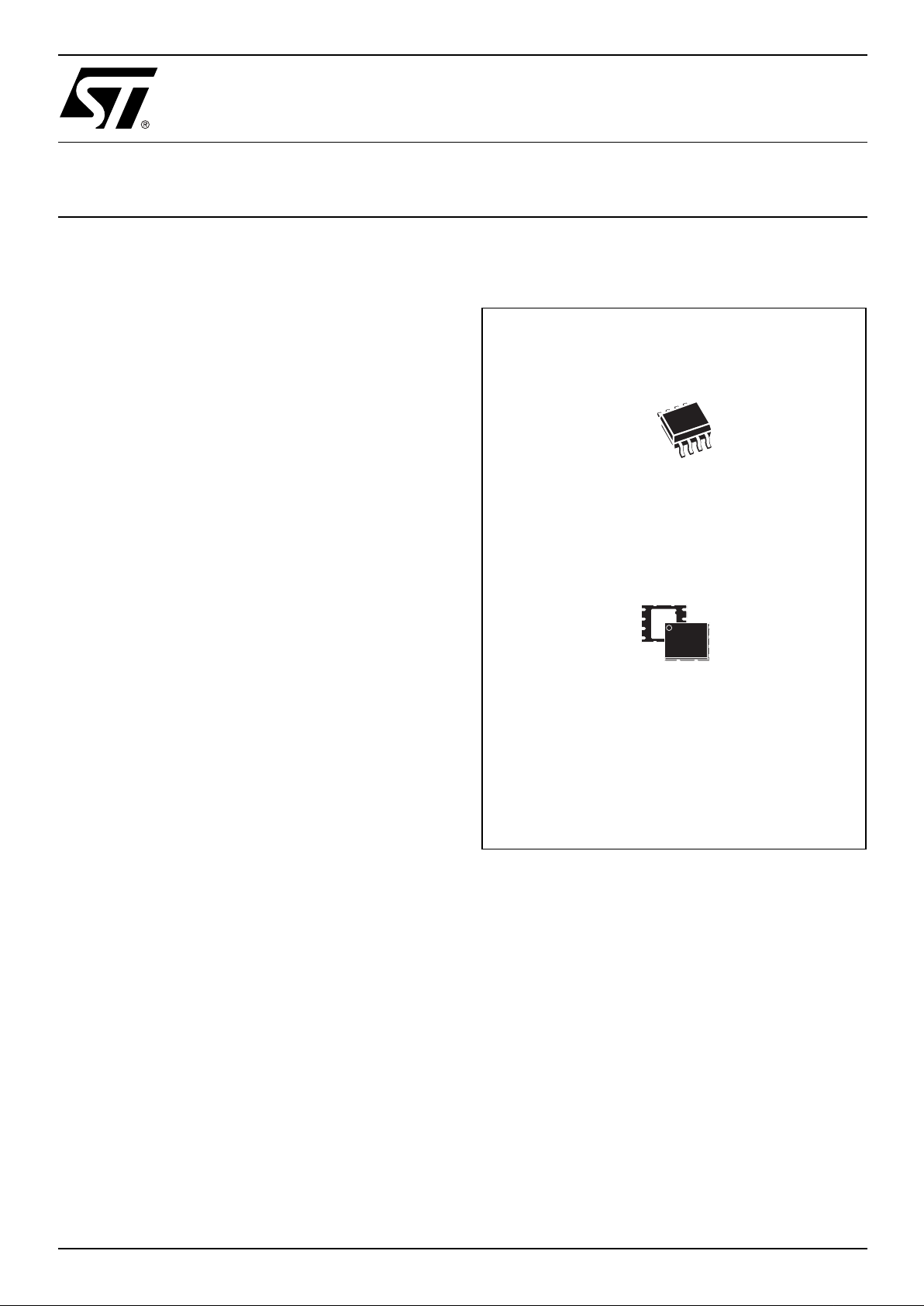
Figure 1. Packages
SO8 (MN)
150 mil width
8
1
VFQFPN8 (MP)
(MLP8)
Page 2
M25P40
2/35
AI04090
S
V
CC
M25P40
HOLD
V
SS
W
Q
C
D
SUMMARY DESCRIPTION
The M25P 40 is a 4 Mbit ( 512K x 8) S erial Flash
Memory, with advanced write protection mechanisms, accessed by a high spee d SPI-comp atible
bus.
The memory can be programmed 1 to 256 bytes at
a time, using the Page Program instruction.
The memory is organized as 8 s ectors, eac h containing 256 pages. Each page is 256 bytes wide.
Thus, the whole memory can be viewed as consisting of 2048 pages, or 524,288 bytes.
The whole mem ory can b e erased using t he Bulk
Erase instruction, or a sector at a time, using the
Sector Erase instruction.
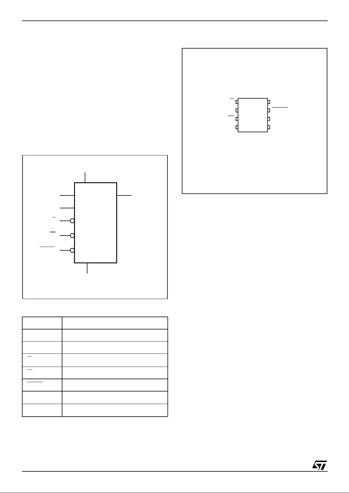
Figure 2. L o gi c D iag ram
Figure 3. SO and VFQFPN Connections
Note: 1. See page 31 (onwards) for package dimensions, and how
to identify pin-1.
Table 1. Signal Names
1
AI04091B
2
3
4
8
7
6
5
DV
SS
C
HOLDQ
SV
CC
W
M25P40
C Serial Clock
D Serial Data Input
Q Serial Data Output
S
Chip Select
W
Write Protect
HOLD
Hold
V
CC
Supply Voltage
V
SS
Ground
Page 3

3/35
M25P40
SIGNAL DESCRIPTION
Serial Data Output (Q). This output signal is
used to transfer data serially out of the device.
Data is shifted out on the falling edge of Serial
Clock (C).
Serial Data Input (D). This input signal is used to
transfer data serially into the device. It receives instructions, addresses, and the data to be programmed. Values are latched on the rising edge of
Serial Clock (C).
Serial Clock (C). This input signal provides the
timing of the serial interface. Instructions, addresses, or data present at Serial Data Input (D) are
latched on the rising edge of Serial Clock (C). Data
on Serial Data Output (Q) changes after the falling
edge of Serial Clock (C).
Chip Select (S
). When this input signal is High,
the device is deselected and Serial Da ta Output
(Q) is at high impedance. Unless an internal Program, Erase or Write Status Register cycle is in
progress, the device w ill be in the Standby mode
(this is not the Deep Power-down mode). D riving
Chip Selec t ( S
) Low enables the device, placing it
in the active power mode.
After Power-up, a falling edge on Chip Select (S
)
is required prior to the start of any instruction.
Hold (HOLD
). The Hold (HOLD) signal is used to
pause any serial communications with the device
without deselecting the device.
During the Hold condition, the Serial Data Output
(Q) is high imp edance, and Seria l Data Input (D)
and Serial Clock (C) are Don’t Care.
To start the Hold condition, the device must be se-
lected, wit h C hip S ele c t ( S
) driven Low.
Write Protect (W
). The main purpose of this in-
put signal is to freeze the size of the area of memory that is protected against program or erase
instructions (as specified by the values in the BP2,
BP1 and BP0 bits of the Status Register).
Page 4
M25P40
4/35
SPI MODES
These devices can be dri ven by a microc ontroller
with its SPI periphe ra l running in ei ther of the two
following modes:
– CPOL=0, CPHA=0
– CPOL=1, CPHA=1
For these two modes, input data is latched in on
the rising edge of Serial Clock (C), and output data
is avai lable from t he falling edge of S erial Clock
(C).
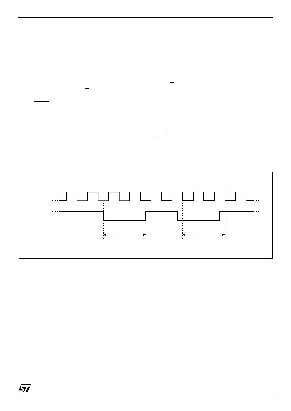
The difference between the two modes, as shown
in Figure 5, is the clock polarity when the bus master is in Stand-by mode and not transferring data:
– C remains at 0 for (CPOL=0, CPHA=0)
– C remains at 1 for (CPOL=1, CPHA=1)
Figure 4. Bus Master and Memory Devices on the SPI Bus
Note: 1. The Wri te Protect (W) a nd Hold (HOLD ) signals should be dr i ven, High or Low as appropriate.
Figure 5. SPI Modes Sup po rt ed
AI03746D
Bus Master
(ST6, ST7, ST9,
ST10, Others)
SPI Memory
Device
SDO
SDI
SCK
CQD
S
SPI Memory
Device
CQD
S
SPI Memory
Device
CQD
S
CS3 CS2 CS1
SPI Interface with
(CPOL, CPHA) =
(0, 0) or (1, 1)
W
HOLD
W
HOLD
W
HOLD
AI01438B
C
MSB
CPHA
D
0
1
CPOL
0
1
Q
C
MSB
Page 5

5/35
M25P40
OPERATING FEATURES
Page Prog ra m m i ng
To program one data byte, two instructions are required: Write Enable (WREN), which is on e byte,
and a Page Program (PP) sequence, which consists of four bytes plus data. This is followed by the
internal Program cycle (of duration t
PP
).
To spread this overhead, the Page P rogram (PP)
instruction allows up to 256 bytes to be programmed at a time (changing bits from 1 to 0), provided that they lie in consecutive addresses on the
same page of memory.
Sector Erase and Bulk Erase
The Page Program (PP) instruction allows bits to
be reset from 1 to 0. Before this can be applied, the
bytes of memory need to hav e been erase d to all
1s (FFh). This can be achieved either a sector at a
time, using the Sector Erase (SE) instruction, or
throughout the entire memory, using the Bulk
Erase (BE) instruction. This starts an internal
Erase cycle (of duration t
SE
or tBE).
The Erase instruction must be preceeded by a
Write Enable (WREN) instruction.
Polling During a Write, Program or Erase Cycle
A further improvement in the time to Write Status
Register (WRSR), Program (PP) or Erase (SE or
BE) can be achieved by not waiting for the worst
case delay (t
W
, tPP, tSE, or tBE). The Write In
Progress (WIP) bit is provided in the Status Register so that the application program can monitor its
value, polling it to establish when the previous
Write cycle, Program cycle or Erase cycle is complete.
Activ e Power, Stand-b y Power and De ep
Power-Down Modes
When Chip Select (S) is Low, the device is enabled, and in the Active Power mode.
When Chip Select (S
) is High, the device is disabled, but could remain in the Active Power mode
until all internal cycles have completed (Program,
Erase, Write Status Register). The device then
goes in to the Stand-by P ower mode. T he device
consumption drops to I
CC1
.
The Deep Power-down mode is entered when the
specific instruction (the Enter Deep Power-down
Mode (DP) instruction) is executed. The device
consumption drops further to I
CC2
. The device remains in this mode until another specific instruction (the Release from Deep Power-down Mode
and Read Elect ronic Signature (RE S) ins truction)
is executed.
All other instructions are ignored while the device
is in the Deep Power-down mode. This can be
used as an extra software protectio n mechanism,
when the device is not in active use, to protect the
device from inadvertant Wri te, Program or Erase
instructions.
Status Register
The Status Register contains a num ber of status
and control bits that can be read or set (as appropriate) by specific instructions.
WIP bit. The Write In Progress (WIP) bit indicates
whether the memory is busy with a Write S tatus
Register, Program or Erase cycle.
WEL bit. The Write E nable Latch (W EL) bit indicates the status of the internal Write Enable Latch.
BP2, BP1, BP0 bits. The Block Protect (BP2,
BP1, BP0) bits are non-volatile. They define the
size of the area to be software protected against
Program and Erase instructions.
SRWD bit. The Status Register Write Disable
(SRWD) bit is operated in conjunction with the
Write Protect (W
) signal. The Status Register
Write Disable (SRWD) bit an d Write Protect (W
)
signal allow the device to be put in the Hardware
Protected mode. In this mode, the non-volatile bits
of the Status Register (SRWD, BP2, BP1, BP0)
become read-only bits.
Page 6
M25P40
6/35
Prot ection Modes
The environments where non-volatile memory devices are used can be very noisy. No SPI dev ice
can operate correctly in the presence of excessive
noise. To help combat this, the M25P40 boasts the
following data protection mechanisms:
■ Power-On Reset and an internal timer (t
PUW
)
can provide protection against inadvertant
changes while the power supply is outside the
operating specification.
■ Program, Erase and Write Status Register
instructions are checked that they consist of a
number of clock pulses that is a multiple of
eight, before they are accepted for execution.
■ All instructions that modify data must be
preceded by a Write Enable (WREN) instruction
to set the Write Enable Latch (WEL) bit . This bit
is returned to its reset state by the following
events:
– Power-up
– Write Disable (WRDI) instruction completion
– Write Status Register (WRSR) instruction
completion
– Page Program (PP) instruction completion
– Sector Erase (SE) instruction completion
– Bulk Erase (BE) instru ction completi on
■ The Block Protect (BP2, BP1, BP0) bits allow
part of the memory to be configured as readonly. This is the Software Protected Mode
(SPM).
■ The Write Protect (W) signal allows the Block
Protect (BP2, BP1, BP0) bits and Status
Register Write Disable (SRWD) bit to be
protected. This is the Hardware Protected Mode
(HPM).
■ In addition to the low power consumption
feature, the Deep Power-down mode offers
extra software protection from inadvertant
Write, Program and Erase instructions, as all
instructions are ignored except one particular
instruction (the Release from Deep Powerdown instruction).
Table 2. Protected Area Sizes
Note: 1. The device is ready t o accept a Bu l k E rase instruction if, and only if, all B l ock Protect (B P2, BP1, BP0) are 0.
Status Register
Content
Memory Content
BP2
Bit
BP1
Bit
BP0
Bit
Protected Area Unprotected Area
0 0 0 none
All sectors
1
(eight sectors: 0 to 7)
0 0 1 Upper eighth (Sector 7) Lower seven-eighths (seven sectors: 0 to 6)
0 1 0 Upper quarter (two sectors: 6 and 7) Lower three-quarters (six sectors: 0 to 5)
0 1 1 Upper half (four sectors: 4 to 7) Lower half (four sectors: 0 to 3)
1 0 0 All sectors (eight sectors: 0 to 7) none
1 0 1 All sectors (eight sectors: 0 to 7) none
1 1 0 All sectors (eight sectors: 0 to 7) none
1 1 1 All sectors (eight sectors: 0 to 7) none
Page 7
7/35
M25P40
Hold Condition
The Hold (HOLD
) signal is used to pause any serial communications with the device without resetting the clocking sequence. However, taking this
signal Low does not terminate any Write Status
Register, Program or Erase cycle that is currently
in progress.
To enter the Hold condition, the device must be
selecte d, w it h C hip Select (S
) Low.
The Hold condition starts on the falling edge of the
Hold (HOLD
) signal, provided t hat this coincides
with Serial Clock (C) being L ow (as shown in Figure 6).
The Hold condition ends on the rising edge of the
Hold (HOLD
) signal, provided t hat this coincides
with Serial Clock (C) being Low.
If the falling edge does not coincide with Serial
Clock (C) being Low, the Hold condition starts after Serial Clock (C) next goes Low. Similarly, if the
rising edge does not coincide with Serial Clock (C)
being Low, the Hold condition ends after Serial
Clock (C) next goes Low. (This is shown in Figure
6).
During the Hold condition, the Serial Data Output
(Q) is high imp edance, and Seria l Data Input (D)
and Serial Clock (C) are Don’t Care.
Normally, the device is kept selected, with Chip
Select (S
) driven Low, for the whole duration of the
Hold condition. This is to en sure that the s tate of
the internal logic remains unchanged from the moment of entering the Hold condition.
If Chip Select (S
) goes High while t he d evice is in
the Hold condition, this has the effect of res etting
the internal logic of the device. To restart communication with the device, it is necessary to drive
Hold (HOLD
) High, and then to drive Chip Select
(S
) Low. This prevents the device from going back
to the Hold condition.
Figure 6. Hold Condition Activation
AI02029D
HOLD
C
Hold
Condition
(standard use)
Hold
Condition
(non-standard use)
Page 8
M25P40
8/35
MEMOR Y ORGANIZATI ON
The memory is organized as:
■ 524,288 bytes (8 bits each)
■ 8 sectors (512 Kbits, 65536 bytes each)
■ 2048 pages (256 bytes each).
Each page can be individually programmed (bits
are programmed from 1 to 0). The device is Sector
or Bulk Erasable (bits are erased from 0 to 1) but
not Page Erasable.
Table 3. Memory Organization
Sector Address Range
7 70000h 7FFFFh
6 60000h 6FFFFh
5 50000h 5FFFFh
4 40000h 4FFFFh
3 30000h 3FFFFh
2 20000h 2FFFFh
1 10000h 1FFFFh
0 00000h 0FFFFh
Page 9
9/35
M25P40
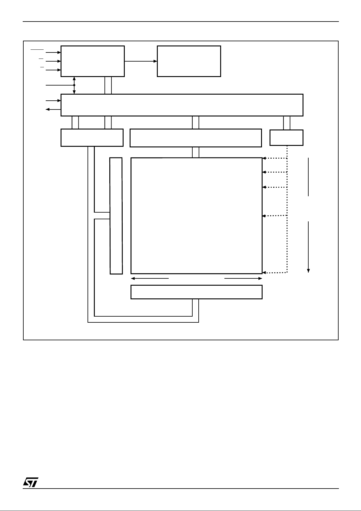
Figure 7. B lo ck Diagram
AI04986
HOLD
S
W
Control Logic
High Voltage
Generator
I/O Shift Register
Address Register
and Counter
256 Byte
Data Buffer
256 Bytes (Page Size)
X Decoder
Y Decoder
Size of the
read-only
memory area
C
D
Q
Status
Register
00000h
7FFFFh
000FFh
Page 10
M25P40
10/35
INSTRUCTIONS
All instructions, addresses and data are shifted in
and out of the device, most significant bit first.
Serial Data Input (D) is sampled on the first rising
edge of Serial Cl ock (C) after Chip Select (S
) is
driven Low. Then, the one-byte instruction code
must be shifted in to the device, most significant bit
first, on Serial Data Input (D), each bit being
latched on the rising edges of Serial Clock (C).
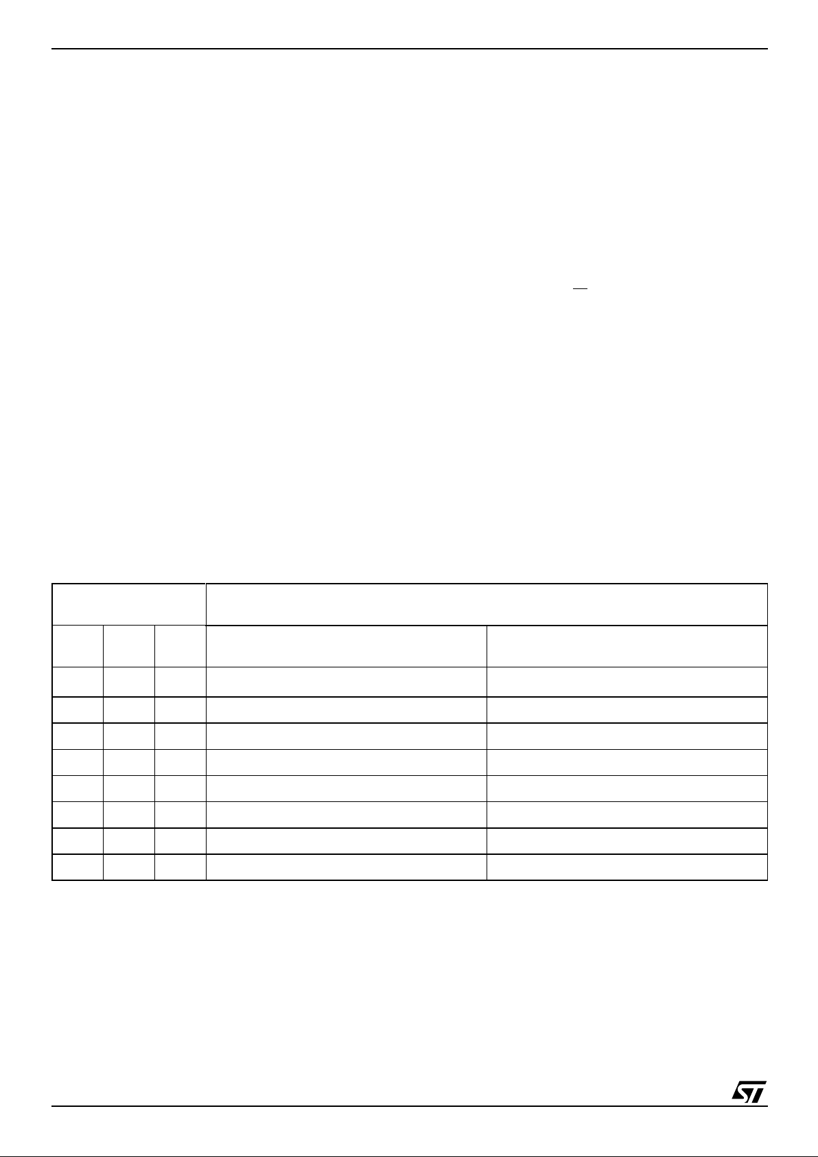
The instruction set is listed in Table 4.
Every instruction sequence starts with a one-byte
instruction code. Depending on the instruction,
this might be followed by address bytes, or by data
bytes, or by both or none. Chip Select (S
) must be
driven High after the last bit of the instruction sequence has been shifted in.
In the case of a Read Data Bytes (READ), Read
Data Bytes at Higher Speed (Fast_Read), Read
Status Register (RDSR) or Release from Deep
Power-down, and Read Electronic Signature
(RES) instruction, the shifted-in instruction sequence is followed by a data-ou t sequence. Chip
Selec t (S
) can be driven High after any bit of the
data-out sequence is being shifted out.
In the case of a Page Program (PP), Sector Erase
(SE), Bulk Erase (BE), Write Status Register
(WRSR), Write Enable (WREN), Write Disable
(WRDI) or Deep Power-down (DP) instruction,
Chip Sele ct (S
) must be driven High exactly at a
byte boundary, otherwise the instruction is rejected, and is not executed. That is, Chip Select (S
)
must driven High when the number of clock pulses
after Chip Select (S
) being driven Low is an exact
multiple of eight.
All attempts to ac cess the memory array du ring a
Write Status Register cycle, Program cycle or
Erase cycle are ignored, and the internal Write
Status Register cycle, Program cycle or Erase cycle continues unaffected.
Table 4. Instruction Set
Instruction Description One-byte Instruction Code
Address
Bytes
Dummy
Bytes
Data
Bytes
WREN Write Enable 0000 0110 0 0 0
WRDI Write Disable 0000 0100 0 0 0
RDSR Read Status Register 0000 0101 0 0 1 to
∞
WRSR Write Status Register 0000 0001 0 0 1
READ Read Data Bytes 0000 0011 3 0 1 to
∞
FAST_READ Read Data Bytes at Higher Speed 0000 1011 3 1 1 to
∞
PP Page Program 0000 0010 3 0 1 to 256
SE Sector Erase 1101 1000 3 0 0
BE Bulk Erase 1100 0111 0 0 0
DP Deep Power-down 1011 1001 0 0 0
RES
Release from Deep Power-down,
and Read Electronic Signature
1010 1011
0 3 1 to
∞
Release from Deep Power-down 0 0 0
Page 11
11/35
M25P40
Figure 8. Write Enable (WREN) Instruction Sequenc e
Write Enable (WREN)
The Write Enable (WREN) instruction (Figure 8)
sets the Write Enable Latch (WEL) bit.
The Write Enable Latch (WEL) bit must be set prior to every Page Program (PP), Sector Erase
(SE), Bulk Erase (BE) and Write Status Register
(WRSR) instruction.
The Write Enable (WREN) instruction is entered
by driving Chip Select (S
) Low, sending the in-
struction code, and then driving Chip Select (S
)
High.
Figure 9. Write Disable (WRDI) Instruction Sequence
Write Disable (WRDI)
The Write Disable (WRDI) instruction (Figure 9)
resets the Write Enable Latch (WEL) bit.
The Write Disable (WRDI) instruction is entered by
driving Ch ip Select (S
) Low, sending t he instruc-
tion code, and then driving Chip Select (S
) High.
The Write Enable Latch (WEL) bit is reset under
the following conditions:
– Power-up
– Write Disable (WRDI) instruction completion
– Write Status Register (WRSR) instruction com-
pletion
– Page Program (PP) instruction completion
– Sector Erase (SE) instruction completion
– Bulk Erase (BE) instruction completion
C
D
AI02281E
S
Q
21 34567
High Impedance
0
Instruction
C
D
AI03750D
S
Q
21 34567
High Impedance
0
Instruction
Page 12

M25P40
12/35
Figure 10. Read Status Register (RDSR) Instruction Sequence and Data-Out Sequence
Read Status Register (RDSR)
The Read Status Register (RDSR) instruction allows the Status Register to be read. The Status
Register may be read at any time, even while a
Program, Erase or Write Status Register cycle is in
progress. When one of these cycl es i s in progress,
it is recommended to check the Write In Progress
(WIP) bit before sending a new instruction to the
device. It is also possible to read the S tatus Register continuously, as shown in Figure 10.
Table 5. Status Register Format
The status and cont rol bits of the Stat us Register
are as follows:
WIP bit. The Write In Progress (WIP) bit indicates
whether the memory is busy with a Write S tatus
Register, Program or Erase cycle. When set to 1,
such a cycle is in progress, when reset to 0 no
such cycle is in progr es s.
WEL bit. The Write E nable Latch (W EL) bit indicates the status of the internal Write Enable Latch.
When set to 1 the internal Write Enable Latch is
set, when set to 0 the internal W rite E nabl e Latch
is reset and no W rite Status Register, Program or
Erase instruction is accepted.
BP2, BP1, BP0 bits. The Block Protect (BP2,
BP1, BP0) bits are non-volatile. They define the
size of the area to be software protected against
Program and Erase instructions. These bits are
written with the Write Status Register (WRSR) instruction. When on e or both of the B lock Protect
(BP2, BP1, BP0) bit s i s s et t o 1, the rel evan t me mory area (as defined in Table 2) becom es protec ted against Page Program (PP) and Sector Erase
(SE) instructions. The Block Protect (BP2, BP1,
BP0) bits can be written provided that the Hardware Protected mode has not been s et. The Bulk
Erase (BE) instruction is executed if, and only if,
both Block Protect (BP2, BP1, BP0) bits are 0.
SRWD bit. The Status Register Write Disable
(SRWD) bit is operated in conjunction with the
Write Protect (W
) signal. The Status Register
Write Disable (SRWD) bit an d Write Protect (W
)
signal allow the device to be put in the Hardware
Protected mode (wh en the Status Register Write
Disable (SRWD) bit is set to 1, and Write Protect
(W
) is driven Low). In this mode, the non-volatile
bits of the Status Register (SRWD, BP2, BP1,
BP0) become read-on ly bits an d the W rite Status
Register (WRSR) instruction is no longer accepted
for execution.
C
D
S
21 3456789101112131415
Instruction
0
AI02031E
Q
7 6543210
Status Register Out
High Impedance
MSB
7 6543210
Status Register Out
MSB
7
b7 b0
SRWD 0 0 BP2 BP1 BP0 WEL WIP
Status Register
Write Protect
Block Protect Bits
Write Enable Latch Bit
Write In Progress Bit
Page 13

13/35
M25P40
Figure 11. Write Status Register (WRSR) Instruction Sequenc e
Write Status Register (WRSR)
The Write Status Register (WRSR) instruction allows new values to be written to the Status Register. Before it can be accepted, a Write Enable
(WREN) instruction must previously have been executed. After the Write Enable (WREN) instruction
has been decoded an d executed, the de vice sets
the Write Enable Latch (WEL).
The Write Status Register (WRSR) instruction is
entered by driving Chip Select (S
) Low, followed
by the instruction code and the data byte on Serial
Data Input (D).
The instruction sequence is shown in Figure 11.
The Write Status Register (WRSR) instruction has
no effect on b6, b5, b1 and b0 of the S tatus Register. b6 and b5 are always read as 0.
Chip Select (S
) must be driven High after the
eighth bit of the d ata byte has been latched in. If
not, the Write Status Register (WRSR) i nstruction
is not executed. As soon as Chip Select (S
) is driv-
en High, th e self-ti med Write S tatus Regist er cycl e
(whose duration is tW) is initiated . While the Writ e
Status Register cycle is in progress, the Status
Register may still be read to check the value of the
Write In Progress (WIP) bit. The Write In Progress
(WIP) bit is 1 during the self-timed Write Status
Register cycle, and is 0 when it is completed.
When the cycle is completed, the Write Enable
Latch (WEL) is reset.
The Write Status Register (WRSR) instruction allows the user to change the values of the Block
Protect (BP2, BP1, BP0) bits, to define the size of
the area that is to be treated as read-only, as defined in Table 2. The Write Status Register
(WRSR) instruction also allows the user to set or
reset the Status Register Write Disable (SRWD)
bit in accordance with the Write Protect (W
) signal.
The Status Register Write Disable (SRWD) bit and
Write Protect (W
) signal allow the device to be put
in the Hardware Protected Mode (HPM). The Write
Status Register (WRSR) instruction is not executed once the Ha rdware Protected Mode (HPM) is
entered.
C
D
AI02282D
S
Q
21 3456789101112131415
High Impedance
Instruction Status
Register In
0
765432 0
1
MSB
Page 14

M25P40
14/35
Table 6. Protection Mode s
Note: 1. As defined by the va lu es in the Block Protect (B P2, BP1, BP0) bits of the S tatus Regis ter, as shown in Table 2.
The protection features of t he device are summarized in Table 6.
When the Status Register Write Disable (SRWD)
bit of the Status Register is 0 (its initial delivery
state), it is possible to write to the Status Register
provided that the Write Enable Latch (WEL) bit has
previously been set by a Write Enable (WREN) instruction, regardless of the wheth er Write P rotect
(W
) is driven High or Low.
When the Status Register Write Disable (SRWD)
bit of the Status Register is set to 1, two cases
need to be considered, depending on the state of
Write Protect (W
):
– If Write Protect (W
) is driven High, it is possible
to write to the Status Register provided that the
Write Enable Latch (WEL) bit has previously
been set by a Write Enable (WREN) instruction.
– If Write Protect (W
) is driven Low, it is
not
pos-
sible to write to the Status Re gister
even
if the
Write Enable Latch (WEL) bit has previously
been set by a Write Enable (WREN) instruction.
(Attempts to write to the Status Register are rejected, and are not accepted f or execution). As
a consequence, all the data bytes in the memory area that are software protected (SPM) by the
Block Pro tec t (BP2, BP1, BP0 ) bi ts of th e St atus
Register, are also hardware protected against
data modification.
Regardless of the order of the two events, the
Hardware Protected Mode (HPM) can be entered:
– by setting the Status Register Write Disable
(SRWD) bit after driving Write Protect (W
) Low
– or by driving Write Protect (W
) Low after setting
the Status Register Write Disable (SRWD) bit.
The only way to exit the Hardware Protected Mode
(HPM) once entered is to pull Write Protect (W
)
High.
If Write Protect (W
) is permanently tied High, the
Hardware Protected Mode (HPM) can never be
activated, and on ly the Software Prot ected Mode
(SPM), using the Block Protect (BP2, BP1, BP0)
bits of the Status Register, can be used.
W
Signal
SRWD
Bit
Mode
Write Protection of the
Status Register
Memory Content
Protected Area
1
Unprotected Area
1
10
Software
Protected
(SPM)
Status Register is
Writable (if the WREN
instruction has set the
WEL bit)
The values in the SRWD,
BP2, BP1 and BP0 bits
can be changed
Protected against Page
Program, Sector Erase
and Bulk Erase
Ready to accept Page
Program and Sector
Erase instructions
00
11
01
Hardware
Protected
(HPM)
Status Register is
Hardware write protected
The values in the SRWD,
BP2, BP1 and BP0 bits
cannot be changed
Protected against Page
Program, Sector Erase
and Bulk Erase
Ready to accept Page
Program and Sector
Erase instructions
Page 15

15/35
M25P40
Figure 12. Read Data Bytes (READ) Instruction Sequence and Data-Out Sequence
Note: 1. Address bits A23 to A19 are Don’t Care.
Read Data Bytes (READ)
The device is first sel ec ted by driving Chip S ele ct
(S
) Low. The instruction code for the Read Data
Bytes (READ) instruction is followed by a 3-byte
address (A23-A0), each bit being latched-in during
the rising edge of Serial Clock (C). Then the memory contents, at that address, is shifted out on Serial Data Output (Q), eac h b it bein g shift ed out, at
a maximum frequency f
R
, during the falling edge of
Serial Clock (C).
The instruction sequence is shown in Figure 12.
The first byte addressed can be at any location.
The address is automatically incremented to the
next higher address after each byte of data is shift ed out. The whole memory can, t herefore, be read
with a single Read Data Byt es (READ) i nst ruction.
When the highest address is reached, the address
counter rolls over to 000000h, allowing the read
sequence to be continued indefinitely.
The Read Data Bytes (READ) instruction is terminated by driving Chip Select (S
) High. Chip Select
(S
) can be driven High at any time during data output. Any Read Data Bytes (READ) instruction,
while an Erase, Program or Write cycle is in
progress, is rejected without having any effects on
the cycle that is in pro gr es s.
C
D
AI03748D
S
Q
23
21 345678910 2829303132333435
2221 3210
36 37 38
76543 1 7
0
High Impedance
Data Out 1
Instruction 24-Bit Address
0
MSB
MSB
2
39
Data Out 2
Page 16

M25P40
16/35
Figure 13. Read Data Bytes at Higher Speed (FAST_READ) Instruction Sequence and Data-Out
Sequence
Note: 1. Address bits A23 to A19 are Don’t Care.
Read Data Bytes at Higher Speed
(FAST_READ)
The device is first sel ec ted by driving Chip S ele ct
(S
) Low. The instruction code for the Read Data
Bytes at Higher Speed (FAST_READ) i nstruction
is followed by a 3-byte address (A23-A0) and a
dummy byte, each bit bein g latched-in during the
rising edge of Serial Clock (C). Then the memory
contents, at that address, is shifted out on Se rial
Data Output (Q), each bit bein g shifted out, at a
maximum frequency f
C
, during the falling edge of
Serial Clock (C).
The instruction sequence is shown in Figure 13.
The first byte addressed can be at any location.
The address is automatically incremented to the
next higher address after each byte of data is shift ed out. The whole memory can, t herefore, be read
with a single Read Data Bytes at Higher Speed
(FAST_READ) instruction. When the highest address is reached, the address counter rolls over to
000000h, allowing the read sequence to be continued indefinitely.
The Read Data Bytes at Higher Speed
(FAST_READ) instruction is terminated by driving
Chip Select (S
) High. Chip Select (S) can be driven High at any time during data output. Any Read
Data Bytes at Higher Speed (FAST_READ) instruction, while an Erase, Program or Write cycle
is in progress, is rejected without having any effects on the cycle that is in progress.
C
D
AI04006
S
Q
23
21 345678910 28293031
2221 3210
High Impedance
Instruction 24 BIT ADDRESS
0
C
D
S
Q
32 33 34 36 37 38 39 40 41 42 43 44 45 46
765432 0
1
DATA OUT 1
Dummy Byte
MSB
7 6543210
DATA OUT 2
MSB MSB
7
47
765432 0
1
35
Page 17

17/35
M25P40
Figure 14. Page Program (PP) Instruction Sequence
Note: 1. Address bits A23 to A19 are Don’t Care.
Page Program (PP)
The Page Program (PP) instruction allows bytes to
be programmed in the memory (changing bits from
1 to 0). Before it can be acc epted, a Wri te Enable
(WREN) instruction must previously have been executed. After the Write Enable (WREN) instruction
has been decoded, the device sets the Write Enable Latch (WEL).
The Page Program (PP) instruction is ent ered by
driving Chip Select (S
) Low, followed by the instruction code, three address bytes and at least
one data byte on Serial Data Input (D). If the 8
least significant address bits (A7-A0) are not all
zero, all transmitted data that goes beyond the end
of the current page are programmed from the start
address of the same page (from the address
whose 8 least significant bits (A7-A0) are all zero).
Chip Selec t (S
) must be driven Low for the entire
duration of the sequence.
The instruction sequence is shown in Figure 14.
If more than 256 bytes are sent to the device, pre-
viously latched data are discarded and the last 256
data bytes are guaranteed to be programmed correctly within the same page. If less than 256 Data
bytes are sent to device, they are correctly programmed at the requested addresses without having any effects on the other bytes of the same
page.
Chip Select (S
) must be driven High after the
eighth bit of the last data byte has been latched in,
otherwise the Page Program (PP) instruction is not
executed.
As soon as Chip Select (S
) is driv en H i gh , th e s el f -
timed Page Pr ogram cycle (whose duration is t
PP
)
is initiated. While the Page Program cycle is in
progress, the Status Register may be read to
check the value of the Write In Progress (WIP) bit.
The Write In Progress (WIP) bit is 1 during the selftimed Page Program cycle, and is 0 when it is
completed. At some unspecified time before the
cycle is completed, the Write Enable Latch (WEL)
bit is reset.
A Page Program (PP) instruction applied to a page
which is protected by the Block Protect (BP2, BP1,
BP0) bits (see Tables 3 and 2) is not executed.
C
D
AI04082B
S
4241 43 44 45 46 47 48 49 50 52 53 54 5540
C
D
S
23
21 345678910 2829303132333435
2221 3210
36 37 38
Instruction 24-Bit Address
0
765432 0
1
Data Byte 1
39
51
765432 0
1
Data Byte 2
765432 0
1
Data Byte 3 Data Byte 256
2079
2078
2077
2076
2075
2074
2073
765432 0
1
2072
MSB
MSB
MSB MSB MSB
Page 18

M25P40
18/35
Figure 15. Sector Erase (SE) Instruction Sequence
Note: 1. Address bits A23 to A19 are Don’t Care.
Sector Erase (SE)
The Sector Erase (SE) instruction sets to 1 (FFh)
all bits inside the chosen sector. Bef ore it can be
accepted, a Write Enable (WREN) instruction
must previously have been executed. After the
Write Enable (WREN) instruction has been decoded, the device sets the Write Enable Latch (WEL).
The Sector Erase (SE) instruction is entered by
driving Chip Select (S
) Low, followed by the instruction code, and three address bytes on Se rial
Data Input (D). Any address inside the Sector (see
Table 3) is a valid address for the Sector Erase
(SE) instruction. Chip Select (S
) must be driven
Low for the entire duration of the sequence.
The instruction sequence is shown in Figure 15.
Chip Select (S
) must be driven High after the
eighth bit of the last address byte has been latched
in, otherwise the Sector Erase (SE ) instruction is
not executed. As soon as Chip Select (S
) is driven
High, the se lf-timed Secto r Erase cycle (wh ose duration is t
SE
) is initiated. While the Sector Erase cycle is in progress, the Status Register may be read
to check the value of the Write In Progress (WIP)
bit. The Write In Progress (WIP) bit is 1 during the
self-timed Sector Erase cycle, and is 0 when it is
completed. At some unspecified time before the
cycle is completed, the Write Enable Latch (WEL)
bit is reset.
A Sector Erase (S E ) in struction applied to a page
which is protected by the Block Protect (BP2, BP1,
BP0) bits (see Tables 3 and 2) is not executed.
24 Bit Address
C
D
AI03751D
S
21 3456789 293031
Instruction
0
23 22 2 0
1
MSB
Page 19

19/35
M25P40
Figure 16. Bulk Erase (BE) Instruction Sequence
Bulk Erase ( B E)
The Bulk Erase (BE) instruction sets all bits to 1
(FFh). Before it can be accepted, a Write Enab le
(WREN) instruction must previously have been executed. After the Write Enable (WREN) instruction
has been decoded, the device sets the Write Enable Latch (WEL).
The Bulk Erase (BE) instruction is entered by driving Chip Select (S
) Low, followed by the instruction
code on Serial Data Input (D). Chip Select (S
)
must be driven Low for the entire duration o f the
sequence.
The instruction sequence is shown in Figure 16.
Chip Select (S
) must be driven High after the
eighth bit of the instruction code has been latched
in, otherwise the Bulk Erase instruction is not executed. As soon as Chip Select (S
) is driven High,
the self-ti med Bu l k Era se cycle (whose duration i s
t
BE
) is initiated. While the Bulk Erase cycle is in
progress, the Status Register may be read to
check the value of the Write In Progress (WIP) bit.
The Write In Progress (WIP) bit is 1 during the selftimed Bulk Erase cycle , and is 0 when it is completed. At some unspecified time before the cycle
is completed, the Write Enable Latch (WEL) bit is
reset.
The Bulk Erase (BE) instruction is executed only if
all Block Protect (BP2, BP1, BP0) bits are 0. The
Bulk Erase (BE) instruction is ignored if one, or
more, sectors are protected.
C
D
AI03752D
S
21 345670
Instruction
Page 20

M25P40
20/35
Figure 17. Deep Power-down (DP) Instruction Sequence
Deep Power-down (DP)
Executing the Deep Power-down (DP) instruction
is the only way to put the device in the lowest consumption mode (the Deep Power-down mode). It
can also be used as an ext ra software protection
mechanism, while the device is not in active use,
since in this mode, the device ignores all Write,
Program and Erase instructions.
Driving Chip Select (S
) High deselects the device,
and puts the device in the Standby m ode (if there
is no internal cycle currently in progress). But this
mode is not the Deep Power-down mode. The
Deep Power-down mode can onl y be entered by
executing the Deep Power-down (DP) instruction,
to reduce the standby current (from I
CC1
to I
CC2
,
as specified in Table 12).
Once the device has entered the Deep Power-
down mode, all instructions are ignored except the
Release from Deep Power-down and Read Electronic Signature (RES) instruction. This releases
the device from this mode. The Release from
Deep Power-down and Read Electronic Signature
(RES) instruction also allows the Electronic Signa-
ture of the device to be output on Serial Data Output (Q).
The Deep Power-down m ode automaticall y stops
at Power-down, and the device always Powers-up
in the Standby mode.
The Deep Power-down (DP) instruction is entered
by driving Chip Select (S
) Low, followed by the instruction code on Se rial Data Input (D). Chip Select (S
) must be driven Low for the entire duration
of the sequence.
The instruction sequence is shown in Figure 17.
Chip Select (S
) must be driven High after the
eighth bit of the instruction code has been latched
in, otherwise the Deep Power-down (DP) instruction is not executed. As soon as Chip Select (S
) is
driven High, it requires a delay of t
DP
before the
supply current is reduced to I
CC2
and the Deep
Power-down mode is entered.
Any Deep Power-down (DP) ins truction, while an
Erase, Program or Write cycle is in progress, is rejected witho ut havin g any eff ec ts on the cycle that
is in progress.
C
D
AI03753D
S
21 345670
t
DP
Deep Power-down Mode
Stand-by Mode
Instruction
Page 21

21/35
M25P40
Figure 18. Release from Deep Power-down and Read Electronic Signatur e (RES) Instruction
Sequence and Data-Out Sequ e nce
Release from Deep Power-down and Read
Electronic Signature (RES)
Once the device has entered the Deep Powerdown mode, all instructions are ignored except the
Release from Deep Power-down and Read Electronic Signature (RES) instruction. Executing this
instruction takes the device out of the Deep Power-down mode. The instruction can also be used to
read, on Serial Data Output (Q), the 8-bit Electronic Signature of the device.
Except while an Erase, Program or Write Status
Register cycle is in progress, the Release from
Deep Power-down and Read Electronic Signature
(RES) instruction always provides access to the
Electronic Signature of the device, and can be applied even if the Deep Power-down mode has not
been entered.
Any Release from Deep Power-down and Read
Electronic Signature (RES) instruction while an
Erase, Program or Write Status Register cycle is in
progress, is not decoded, and has no effect on the
cycle that is in progress.
This instruction serves a second purpose. The device features an 8-bit Electronic Signature, whose
value for the M25P40 is 12h. This can be read using the Release from Deep Power-down and Read
Electronic Signature (RES) instruction.
The device is first sel ec ted by driving Chip S el ect
(S
) Low. The instruction code is followed by 3
dummy bytes, each bit being latched-in on Serial
Data Input (D) during the rising edge of Serial
Clock (C). Then, the 8-bit Electronic Signature,
stored in the memory, is shifted out on Serial Data
Output (Q), each bit being s hifted out during the
falling edge of Serial Clock (C).
The instruction sequence is shown in Figure 18.
The Release from Deep Power-down and Read
Electronic Signature (RES) instruction is terminated by driving Chip Sele ct (S
) High after the Electronic Signature has been read at least once.
Sending additional clock cycles on Serial Clock
(C), while Chip Select (S
) is driven Low, cause the
Electronic Signature to be output repeatedly.
When Chip Select (S
) is driven Hig h, the de v ice is
put in the Stand-by Power mode. If the device was
not previously in the Deep Power-down mode, the
transition to the Stand-by Pow er m ode is immediate. If the device was previously in the Deep Power-down mode, though, the transition to the Standby Power mode is delayed by t
RES2
, and Chip Se-
lect (S
) must remain High for at least t
RES2
(max),
as specified in Table 13. Once in the Stand-by
Power mode, the device waits to be selected, so
that it can receive, decode and execute instructions.
C
D
AI04047C
S
Q
23
21 345678910 2829303132333435
2221 3210
36 37 38
765432 0
1
High Impedance
Electronic Signature Out
Instruction 3 Dummy Bytes
0
MSB
Stand-by Mode
Deep Power-down Mode
MSB
t
RES2
Page 22

M25P40
22/35
Figure 19. Release from Deep Power-down (RES) Instruction Sequence
Driving Chip Select (S
) High after the 8-bit instruction byte has been received by the device, but before the whole of the 8-bit Electronic Signature has
been transmitted for the first time (as shown in Figure 19), still insures that the device is put into
Stand-by Power mode. I f the d evice was not previously in the Deep Power-down mode, the transition to the Stand-by Power mode is immediate. If
the device was previously in the Deep Powerdown mode, though, the transition to the Stand-by
Power mode is delayed by t
RES1
, and Ch ip Select
(S
) must remain High for at least t
RES1
(max), as
specified in Table 13. Once in the Stand-by Power
mode, the device waits to be selected, so that it
can receive, decode and execute instructions.
C
D
AI04078B
S
21 345670
t
RES1
Stand-by Mode
Deep Power-down Mode
Q
High Impedance
Instruction
Page 23

23/35
M25P40
POWER-UP AND POWER-DOWN
At Power-up and Power-down, the device must
not be selected (that is Chip Select (S
) must follow
the voltage applied on V
CC
) until VCC reaches the
correct value:
–V
CC
(min) at Power-up, and then for a further de-
lay of t
VSL
–VSS at Power-down
Usually a simple pull-up resistor on Chip Select (S
)
can be used to insure safe and proper Power-up
and Power-down.
To avoid data corruption and inadvertent write
operations during power up, a Power On Reset
(POR) circuit is included. The logic inside the
device is held reset while V
CC
is less than the POR
threshold value, V
WI
– all operations are disabled,
and the device does not respond to any
instruction.
Moreover, the device ignores all Write Enable
(WREN), Page Program (PP), Sector Erase (SE),
Bulk Erase (BE) and Write Status Register
(WRSR) instructions until a time delay of t
PUW
has
elapsed after the moment that V
CC
rises above the
V
WI
threshold. However, the correct operation of
the device is not guaranteed if, by this time, V
CC
is
still below V
CC
(min). No Write Status Register,
Program or Erase instructions should be sent until
the later of:
–t
PUW
after VCC passed the VWI threshold
–t
VSL
afterVCC passed the VCC(min) level
These values are specified in Table 7.
If the delay, t
VSL
, has elapsed, after VCC has risen
above V
CC
(min), the device can be selected for
READ instructions even if the t
PUW
delay is not yet
fully elapsed.
At Power-up, the device is in the following state:
– The device is in the Standby mode (not the
Deep Power-down mode).
– The Write Enable Latch (WEL) bit is reset.
Normal precautions must be taken for supply rail
decoupling, to stablise the V
CC
feed. Each device
in a system should have the V
CC
rail decoupled by
a suitable capacitor close to the package pins.
(Generally, this capacitor is of the order of 0.1µF).
At Power-down, when V
CC
drops from the
operating voltage, to below the POR threshold
value, V
WI
, all operations are disabled and the
device does not respon d to any instruction. (The
designer needs to be aware that if a Power-down
occurs while a Write, Program or Erase cycle is in
progress, some data corruption can result.)
Figure 20. Power-up Timing
V
CC
AI04009C
VCC(min)
V
WI
Reset State
of the
Device
Chip Selection Not Allowed
Program, Erase and Write Commands are Rejected by the Device
tVSL
tPUW
time
Read Access allowed Device fully
accessible
VCC(max)
Page 24

M25P40
24/35
Table 7. Power-Up Timing and VWI Thresh ol d
Note: 1. These paramet ers are characteri zed only.
INITIAL DELIVERY STATE
The device is delivered with the memory array
erased: all bits are set to 1 (each byte contains
FFh). The Status Register contains 00h (all Status
Register bits are 0).
Symbol Parameter Min. Max. Unit
t
VSL
1
VCC(min) to S low
10 µs
t
PUW
1
Time delay to Write instruction 1 10 ms
V
WI
1
Write Inhibit Voltage 1 2 V
Page 25

25/35
M25P40
MAXIMUM RATI N G
Stressing the de vice above the rating l isted in t he
Absolute Maximum Ratings" table may cause permanent damage to the device. T hese are stress
ratings only and operation of the device at t hese or
any other conditions ab ove thos e indicated i n the
Operating sections of this spec ification is not im-
plied. Exposure to Absolute Maximum Rating conditions for extended periods may affect device
reliability. Refer also to the STMicroelectronics
SURE Program and other relevant quality documents .
Table 8. Absolute Maximum Ratings
Note: 1. IPC/JEDEC J-STD-020A
2. JEDEC Std JE SD 22-A114A (C1=100 pF, R1=1500 Ω, R2=500 Ω)
Symbol Parameter Min. Max. Unit
T
STG
Storage Temperature –65 150 °C
T
LEAD
Lead Temperature during Soldering
(20 seconds max.)
1
SO 235 °C
VFQFPN 235 °C
V
IO
Input and Output Voltage (with respect to Ground) –0.6 4.0 V
V
CC
Supply Voltage –0.6 4.0 V
V
ESD
Electrostatic Discharge Voltage (Human Body model)
2
–2000 2000 V
Page 26

M25P40
26/35
DC AND AC PARAMETERS
This section summarizes t he operating and measurement conditions, and the DC and AC characteristics of the device. The parameters i n the DC
and AC Characteristic tables that follow are derived from tests performed under the Measure-
ment Conditions summarized in the relevant
tables. Designers should c heck that the o perat ing
conditions in their circuit match the m easurement
conditions when relying on the quoted parameters.
Table 9. Operating Conditions
Table 10. AC Measurement Conditions
Note: 1. Outpu t H i- Z i s defined as th e poi nt where data out is no longer driv en.
Figure 21. AC Measurement I/O Waveform
Table 11. Capacitance
Note: Sampl ed only, not 100% tested, at TA=25°C and a frequency of 20 MHz.
Symbol Parameter Min. Max. Unit
V
CC
Supply Voltage 2.7 3.6 V
T
A
Ambient Operating Temperature –40 85 °C
Symbol Parameter Min. Max. Unit
C
L
Load Capacitance 30 pF
Input Rise and Fall Times 5 ns
Input Pulse Voltages
0.2V
CC
to 0.8V
CC
V
Input and Output Timing Reference Voltages
0.3V
CC
to 0.7V
CC
V
Symbol Parameter Test Condition Min. Max. Unit
C
OUT
Output Capacitance (Q) V
OUT
= 0V 8 pF
C
IN
Input Capacitance (other pins) VIN = 0V 6 pF
AI00825B
0.8V
CC
0.2V
CC
0.7V
CC
0.3V
CC
Input and Output
Timing Reference Levels
Input Levels
Page 27

27/35
M25P40
Table 12. DC Characteristics
Table 13. AC Characteristics
Symbol Parameter
Test Condition
(in addition to those in Table 9)
Min. Max. Unit
I
LI
Input Leakage Curren t ± 2 µA
I
LO
Output Leakage Current ± 2 µA
I
CC1
Standby Current
S
= VCC, V
IN
= VSS or V
CC
50 µA
I
CC2
Deep Power-down Current S = VCC, V
IN
= VSS or V
CC
10 µA
I
CC3
Operating Current (READ)
C = 0.1V
CC
/ 0.9.VCC at 25 MHz,
Q = open
4mA
I
CC4
Operating Current (PP) S = V
CC
15 mA
I
CC5
Operating Current (WRSR) S = V
CC
15 mA
I
CC6
Operating Current (SE) S = V
CC
15 mA
I
CC7
Operating Current (BE)
S
= V
CC
15 mA
V
IL
Input Low Voltage – 0.5
0.3V
CC
V
V
IH
Input High Voltage
0.7V
CC
VCC+0.4
V
V
OL
Output Low Voltage IOL = 1.6 mA 0.4 V
V
OH
Output High Voltage
I
OH
= –100µAV
CC
–0.2
V
Test conditions specified in Table 9 and Table 10
Symbol Alt. Parameter Min. Typ. Max. Unit
f
C
f
C
Clock Frequency for the following instructions:
FAST_READ, PP, SE, BE, DP, RES,
WREN, WRDI, RDSR, WRSR
D.C. 25 MHz
f
R
Clock Frequency for READ instructions D.C. 20 MHz
t
CH
1
t
CLH
Clock High Time 18 ns
t
CL
1
t
CLL
Clock Low Time 18 ns
t
CLCH
2
Clock Rise Time3 (peak to peak)
0.1 V/ns
t
CHCL
2
Clock Fall Time3 (peak to peak)
0.1 V/ns
t
SLCH
t
CSS
S Active Setup Time (relative to C) 10 ns
t
CHSL
S Not Active Hold Time (relative to C) 10 ns
t
DVCH
t
DSU
Data In Setup Time 5 ns
t
CHDX
t
DH
Data In Hold Time 5 ns
t
CHSH
S Active Hold Time (relative to C) 10 ns
t
SHCH
S Not Active Setup Time (relative to C) 10 ns
t
SHSL
t
CSH
S Deselect Time 100 ns
t
SHQZ
2
t
DIS
Output Disable Time 15 ns
t
CLQV
t
V
Clock Low to Output Valid 15 ns
Page 28

M25P40
28/35
Note: 1. tCH + tCL must be greater than or equal to 1/ f
C
2. Value guaranteed by characteri zation, not 100% tested i n producti on.
3. Expressed as a slew-rate.
4. Only applicable as a const raint for a WRSR instr uction when SRWD is se t at 1.
t
CLQX
t
HO
Output Hold Time 0 ns
t
HLCH
HOLD Setup Time (relative to C) 10 ns
t
CHHH
HOLD Hold Time (relative to C) 10 ns
t
HHCH
HOLD Setup Time (relative to C) 10 ns
t
CHHL
HOLD Hold Time (relative to C) 10 ns
t
HHQX
2
t
LZ
HOLD to Output Low-Z 15 ns
t
HLQZ
2
t
HZ
HOLD to Output High-Z 20 ns
t
WHSL
4
Write Protect Setup Time 20 ns
t
SHWL
4
Write Protect Hold Time 100 ns
t
DP
2
S High to Deep Power-down Mode 3
µ
s
t
RES1
2
S High to Standby Mode without Electronic
Signature Read
3
µ
s
t
RES2
2
S High to Standby Mode with Electronic
Signature Read
1.8
µ
s
t
W
Write Status Register Cycle Time 5 15 ms
t
PP
Page Program Cycle Time 1.5 5 ms
t
SE
Sector Erase Cycle Time 2 3 s
t
BE
Bulk Erase Cycle Time 5 10 s
Test conditions specified in Table 9 and Table 10
Symbol Alt. Parameter Min. Typ. Max. Unit
Page 29

29/35
M25P40
Figure 22. Serial Input Timing
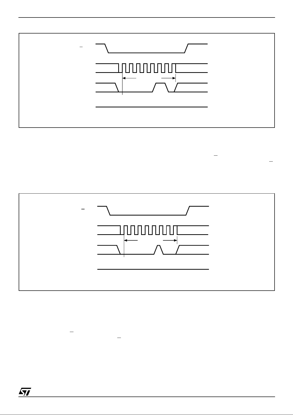
Figure 23. Wri t e Protect Setu p and Hold Tim ing during WRSR when SRWD=1
C
D
AI01447C
S
MSB IN
Q
tDVCH
High Impedance
LSB IN
tSLCH
tCHDX
tCHCL
tCLCH
tSHCH
tSHSL
tCHSHtCHSL
C
D
S
Q
High Impedance
W
tWHSL
tSHWL
AI07439
Page 30

M25P40
30/35
Figure 24. Hold Timing
Figure 25. Output Timing
C
Q
AI02032
S
D
HOLD
tCHHL
tHLCH
tHHCH
tCHHH
tHHQXtHLQZ
C
Q
AI01449D
S
LSB OUT
D
ADDR.LSB IN
tSHQZ
tCH
tCL
tQLQH
tQHQL
tCLQX
tCLQV
tCLQX
tCLQV
Page 31

31/35
M25P40
PACKAGE MECHANICAL
SO8 narrow – 8 lead Plastic Small Outline, 150 mils body width, Package Ou tline
Note: Drawing is not to scale.
SO8 narrow – 8 lead Plastic Small Outline, 150 mils body width, Package M echa ni cal Data
SO-a
E
N
CP
B
e
A
D
C
LA1 α
1
H
h x 45˚
Symb.
mm inches
Typ. Min. Max. Typ. Min. Max.
A 1.35 1.75 0.053 0.069
A1 0.10 0.25 0.004 0.010
B 0.33 0.51 0.013 0.020
C 0.19 0.25 0.007 0.010
D 4.80 5.00 0.189 0.197
E 3.80 4.00 0.150 0.157
e 1.27 – – 0.050 – –
H 5.80 6.20 0.228 0.244
h 0.25 0.50 0.010 0.020
L 0.40 0.90 0.016 0.035
α
0° 8° 0° 8°
N8 8
CP 0.10 0.004
Page 32

M25P40
32/35
VFQFPN8 – 8-contact Very-thin Fine-pitch QFP No-lead, Package Outline
Note: Drawing is not to scale.
VFQFPN8 – 8-contact Very-thin Fine-pitch QFP No-lead, Package Mecha ni cal Data
D
E
VFQFPN-01
A2
A
A3
A1
E1
D1
eE2
D2
L
b
θ
Symb.
mm inches
Typ. Min. Max. Typ. Min. Max.
A 0.85 1.00 0.0335 0.0394
A1 0.00 0.05 0.0000 0.0020
A2 0.65 0.0256
A3 0.20 0.0079
b 0.40 0.35 0.48 0.0157 0.0138 0.0189
D 6.00 0.2362
D1 5.75 0.2264
D2 3.40 3 .20 3.60 0.1339 0.1260 0.1417
E 5.00 0.1969
E1 4.75 0.1870
E2 4.00 3.80 4.20 0.1575 0.1496 0.1654
e 1.27 0.0500
L 0.60 0.50 0.75 0.0236 0.0197 0.0295
θ
12° 12°
Page 33

33/35
M25P40
PART NUMBERING
Table 14. Ordering Information Scheme
For a list of available options (speed, package,
etc.) or for further information on any aspect of this
device, please contact your neares t ST Sales O ffice.
Example: M25P40 –VMN6T
Device Type
M25P
Device Function
40 = 4 Mbit (512K x 8)
Operating Voltage
V = V
CC
= 2.7 to 3.6V
Package
MN = SO8 (150 mil width)
MP = VFQFPN8 (MLP8)
Temperature Range
6 = –40 to 85 °C
Option
T = Tape & Reel Packing
Page 34

M25P40
34/35
REVISION HISTORY
Table 15. Document Revision History
Date Rev. Description of Revision
12-Apr-2001 1.0 Document written
25-May-2001 1.1 Serial Paged Flash Memory renamed as Serial Flash Memory
11-Sep-2001 1.2
Changes to text: Signal Description/Chip Select; Hold Condition/1st para; Protection modes;
Release from Power-down and Read Electronic Signature (RES); Power-up
Repositioning of several tables and illustrations without changing their contents
Power-up timing illustration; SO8W package removed
Changes to tables: Abs Max Ratings/V
IO
; DC Characteristics/V
IL
16-Jan-2002 1.3
FAST_READ instruction added. Document revised with new timings, V
WI
, I
CC3
and clock slew
rate. Descriptions of Polling, Hold Condition, Page Programming, Release for Deep Powerdown made more precise. Value of t
W
(max) modified.
12-Sep-2002 1.4
Clarification of descriptions of entering Stand-by Power mode from Deep Power-down mode,
and of terminating an instruction sequence or data-out sequence.
VFQFPN8 package (MLP8) added. Document promoted to Preliminary Data.
13-Dec-2002 1.5
Typical Page Program time improved. Deep Power-down current changed. Write Protect setup
and hold times specified, for applications that switch Write Protect to exit the Hardware
Protection mode immediately before a WRSR, and to enter the Hardware Protection mode
again immediately after.
12-Jun-2003 1.6 Document promoted from Preliminary Data to full Datasheet
Page 35

35/35
M25P40
Informa tion furnished is believed to be accurate and reliabl e. However, STMicroelectroni cs assumes no responsibili t y for the con sequences
of use of such information nor for any infringement of patents or other rights of third parties which may result from its use. No license is granted
by implication or otherwi se under any patent or patent righ ts of STMic roelectronics. Sp ecificati ons menti oned in th i s publication are subj ect
to change without notice. This publication supersedes and replaces all information previously supplied. STMicroelectronics products are not
authoriz ed for use as c ri t i cal components in life support devices or sy st em s without express wri tten appr oval of STMic roelectro nics.
The ST logo is regis tered trademark of STM i croelec t ronics
All other names are the property of their r espective o wners
© 2003 STMicroelectronics - All Rights Reserved
STMicroelectronics gro up of companies
Australia - Brazi l - Canada - Chin a - F i nl and - Franc e - Germany - Hong Kong -
India - Is rael - Italy - Japan - Malaysia - Malta - Moroc co - Singapore - Spain - Sweden - Swi tz erland - United Kingdom - United States.
www.st.com
 Loading...