

Page 1
1/32
NOT FOR NEW DESIGN
February 2002
This is information on a product still in production but not recommended for new designs.
M25P05
512 Kbit, Low Voltage, Serial Flash Memory
With 20 MHz SPI Bus Interface
FEATURES SUMMARY
This device is now designated as “Not for New Design”. Please use the M25P05-A in all future designs (as described in application note AN1511).
■ 512 Kbit of Flash Memory
■ Page Program (up to 128 Bytes) in 3 ms
(typical)
■ Sector Erase (256 Kbit) in 1 s (typical)
■ Bulk Erase (512 Kbit) in 2 s (typical)
■ 2.7 V to 3.6 V Single Supply Voltage
■ SPI Bus Compatible Serial Interface
■ 20 MHz Clock Rate (maximum)
■ Deep Power-down Mode 1 µA (typ ical)
■ Electronic Signature
■ More than 100,000 Erase/Program Cycles per
Sector
■ More than 20 Year Data Retention
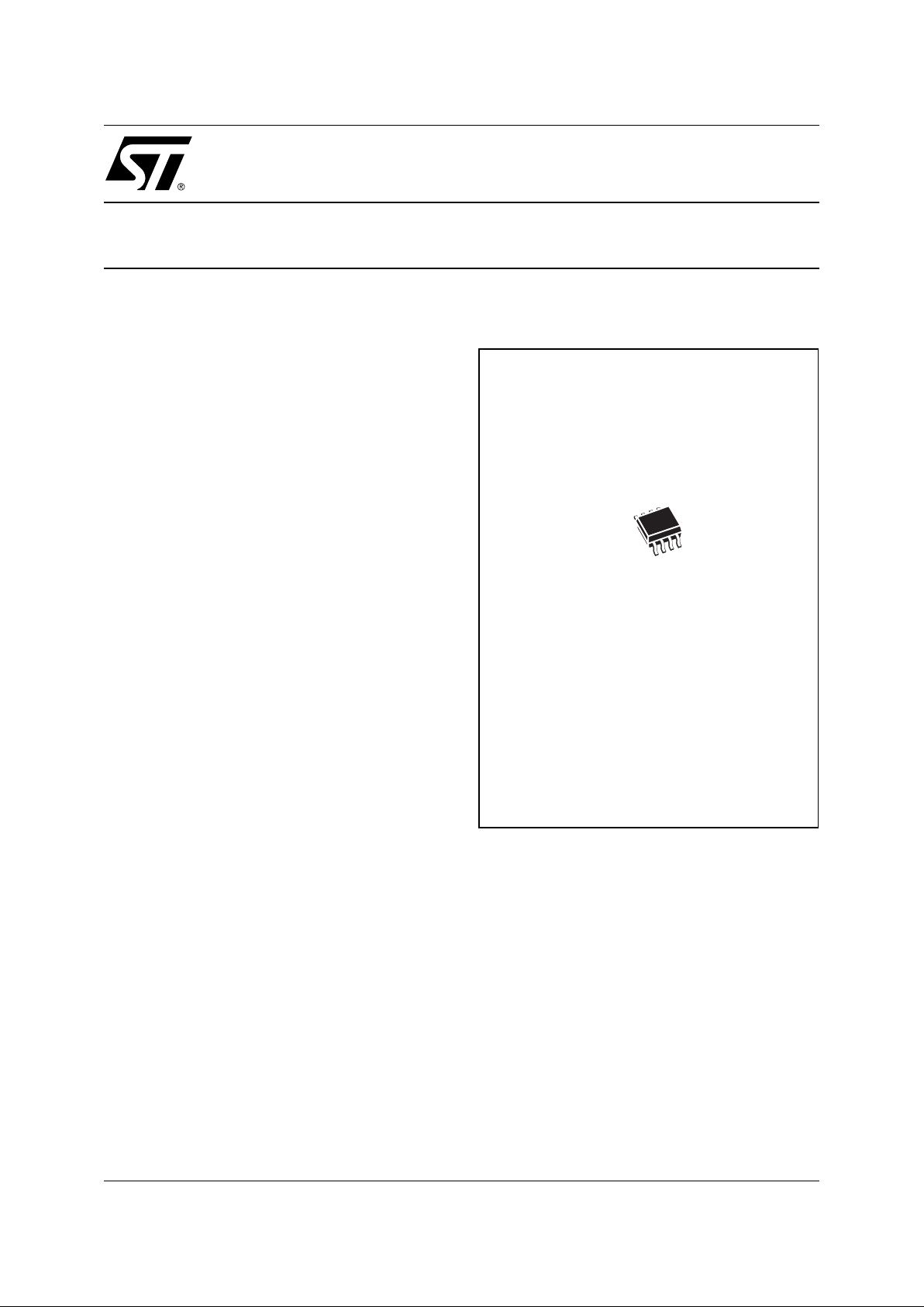
Figure 1. Packages
SO8 (MN)
150 mil width
8
1
Page 2
M25P05
2/32
SUMMARY DESCRIPTION
The M25P05 is a 512 Kbit (64K x 8) Serial Flash
Memory, with advanced write protection mechanisms, accessed by a high spee d SPI-compatible
bus.
The memory can be programmed 1 to 128 bytes at
a time, using the Page Program instruction.
The memory is organized as 2 s ectors, eac h containing 256 pages. E ach page is 128 by tes wide.
Thus, the whole memory can be viewed as consisting of 512 pages, or 65536 bytes.
The whole memory can be eras ed using t he Bulk
Erase instruction, or a sector at a time, us ing the
Sector Erase instruction.
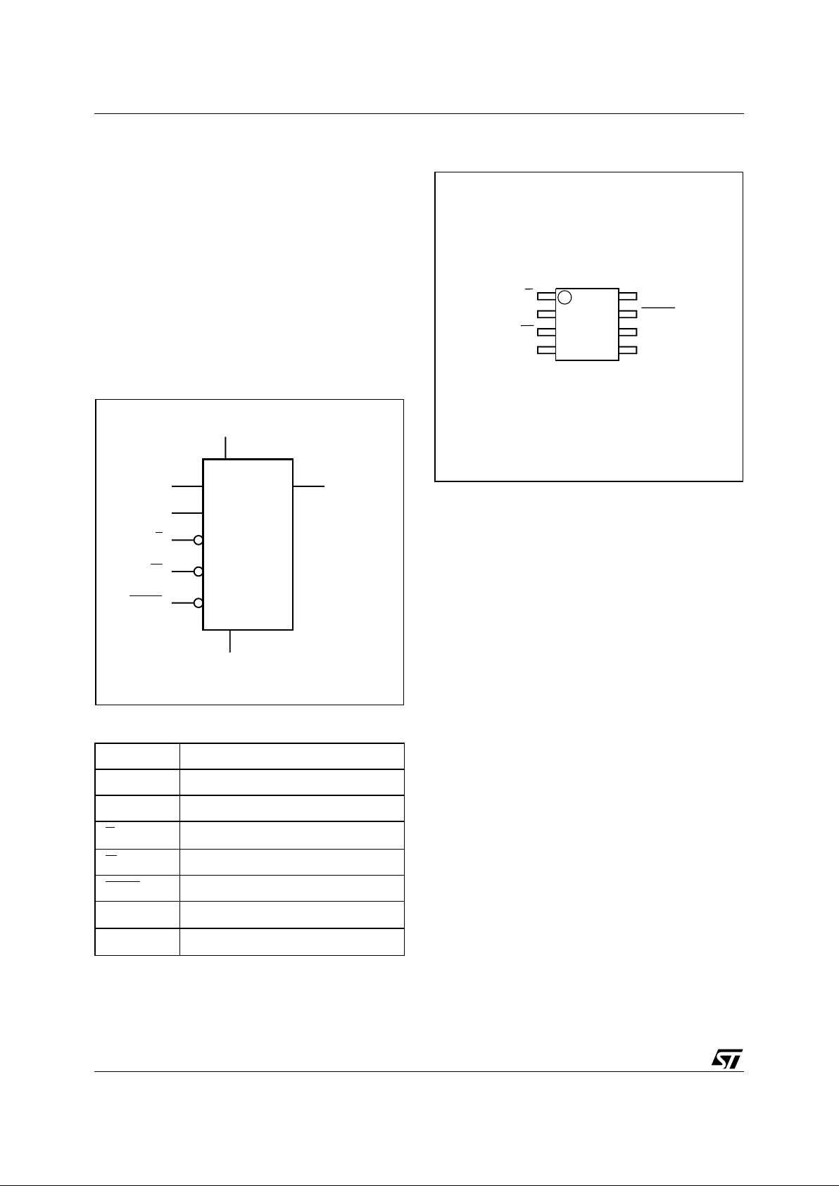
Figure 2. Logic Diagram
Figure 3. SO Connections
Table 1. Signal Names
AI04037
S
V
CC
M25P05
HOLD
V
SS
W
Q
C
D
1
AI04038
2
3
4
8
7
6
5
DV
SS
C
HOLDQ
SV
CC
W
M25P05
C Serial Clock
D Serial Data Input
Q Serial Data Output
S
Chip Select
W
Write Protect
HOLD
Hold
V
CC
Supply Voltage
V
SS
Ground
Page 3

3/32
M25P05
SIGNAL DESCRIPTION
Serial Data Output (Q). This output signal is
used to transfer data serially out of the device.
Data is shifted out on the falling edge of Serial
Clock (C).
Serial Data Input (D). This input signal is used to
transfer data serially into the device. It receives instructions, addresses, and the data to be programmed. Values are latched on the rising edge of
Serial Clock (C).
Serial Clock (C). This input signal provides the
timing of the serial interface. Instructions, addresses, or data present at Serial Data Input (D) are
latched on the rising edge of Serial Clock (C). Data
on Serial Data Output (Q) changes after the falling
edge of Serial Clock (C).
Chip Select (S
). When this input signal is High,
the device is des elected and Serial Data Output
(Q) is at high impedance. Unless an internal Program, Erase or Write Status Register cycle is in
progress, the device will b e in the Standby m ode
(this is not the Deep Power-down mode). D riving
Chip Selec t ( S
) Low enables the device, placing it
in the active power mode.
After Power-up, a falling edge on Chip Select (S
)
is required prior to the start of any instruction.
Hold (HOLD
). The Hold (HOLD) signal is used to
pause any serial communications with the device
without deselecting the device.
During the Hold condition, the Serial Data Output
(Q) is high impedanc e, and Serial D ata Input (D)
and Serial Clock (C) are Don’t Care.
To start the Hold condition, the device must be se-
lected, wit h C h ip S e lec t (S
) driven Low.
Write Protect (W
). The main purpose of this in-
put signal is to freeze the size of the area of memory that is protected against program or erase
instructions (as specified by the values in the BP1
and BP0 bits of the Status Register).
Page 4
M25P05
4/32
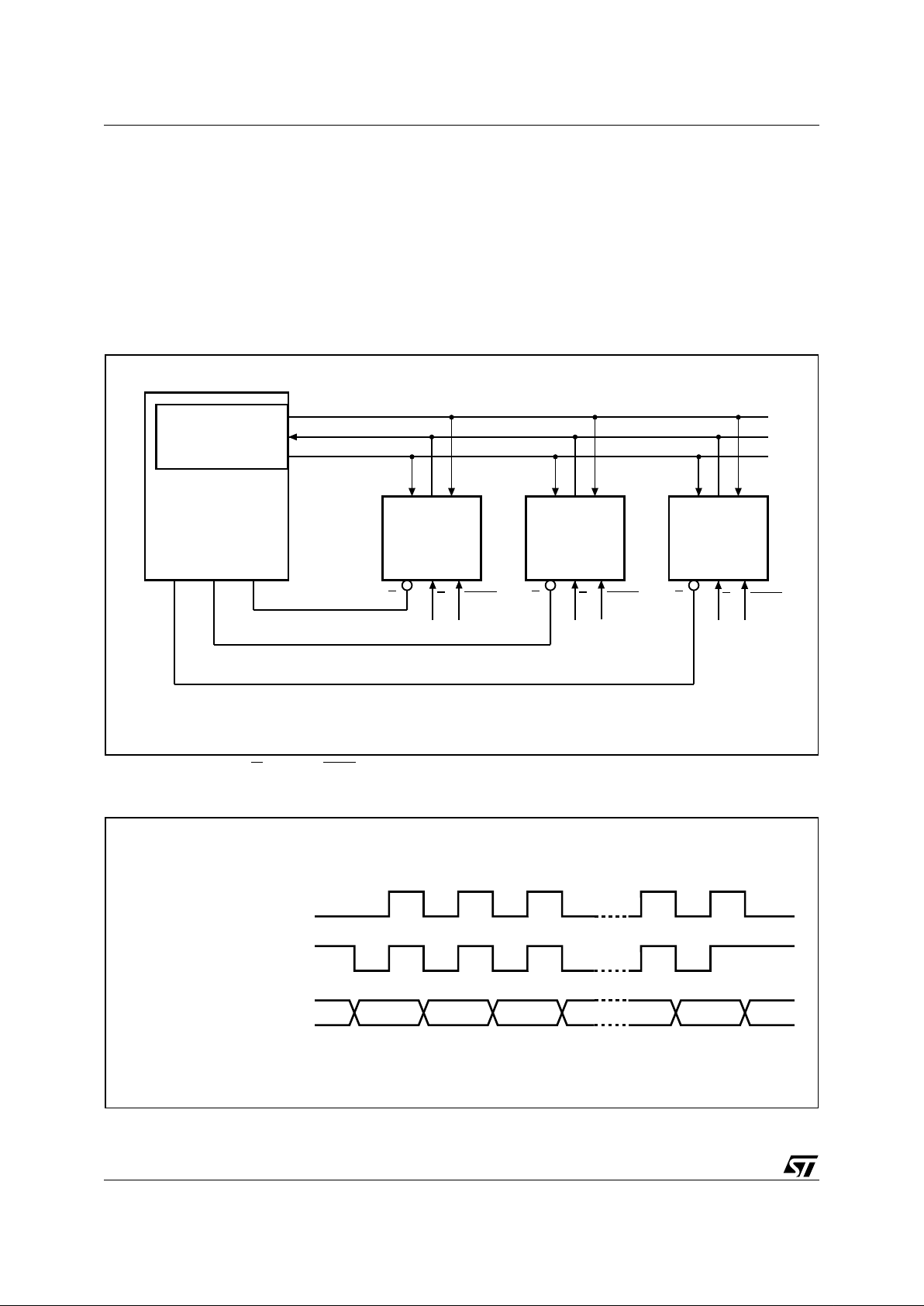
SPI MODES
These devices can be drive n by a microcont roller
with its SPI periphe ral running in ei the r of the two
following modes:
– CPOL=0, CPHA=0
– CPOL=1, CPHA=1
For these two modes, input dat a is latched in on
the rising edge of Serial Clock (C), and output data
is availa ble from t he falling e dge of Se rial Clock
(C).
The difference between the two modes, as shown
in Figure 5, is the clock polarity when the bus master is in Stand-by mode and not transferring data:
– C remains at 0 for (CPOL=0, CPHA=0)
– C remains at 1 for (CPOL=1, CPHA=1)
Figure 4. Bus Master and Memory Devices on the SPI Bus
Note: 1. T he Write Prot ect (W) a nd Hold (HOLD ) signals s hould be driven, High or Low as appropriate.
Figure 5. SPI Mo de s S upported
AI03746C
Bus Master
(ST6, ST7, ST9,
ST10, Others)
SPI Memory
Device
SDO
SDI
SCK
CQD
S
SPI Memory
Device
CQD
S
SPI Memory
Device
CQD
S
CS3 CS2 CS1
SPI Interface with
(CPOL, CPHA) =
(0, 0) or (1, 1)
W
HOLD
W
HOLD
W
HOLD
AI01438
C
C
MSB LSB
CPHA
D or Q
0
1
CPOL
0
1
Page 5

5/32
M25P05
OPERATING FEATURES
Page Prog ram m i ng
To program one data byte, two instructions are required: Write Enable (WREN), which is one by te,
and a Page Program (PP) sequence, which consists of four bytes plus data. This is followed by the
internal Program cycle (of duration t
PP
).
To spread this overhead, the Page P rogram (PP)
instruction allows up to 128 bytes to be programmed at a time (changing bits from 1 to 0), provided that they lie in consecutive addresses on the
same page of memory.
Sector Erase and Bulk Erase
The Page Program (PP) instruction allows bits to
be reset from 1 to 0. Before this can be applied, the
bytes of memory need to have been e rased to a ll
1s (FFh). This can be achieved either a sector at a
time, using the Sector Erase (SE) instruction, or
throughout the entire memory, using the Bulk
Erase (BE) instruction.
Polling During a Write, Program or Erase Cycle
A further improvement in the time to Write Status
Register (WRSR), Program (PP) or Erase (SE or
BE) can be achieved by n ot waiting for the worst
case delay (t
W
, tPP, tSE, or tBE). The Write In
Progress (WIP) bit is provided in the Status Register so that the application program can monitor its
value, polling it to establish when the previous
Write cycle, Program cycle or Erase cycle is complete.
Active Power, Stand-by Power and Deep
Power-Down Modes
When Chip Select (S
) is Low, the device is en-
abled, and in the Active Power mode.
When Chip Select (S
) is High, the device is disabled, but could remain in the Active Power mode
until all internal cycles have completed (Program,
Erase, Write Status Register). The device then
goes in to the Stand-by P ower mode. T he device
consumption drops to I
CC1
.
The Deep Power-down mode is entered when the
specific instruction (the Enter Deep Power-down
Mode (DP) instruction) is executed. The device
consumption drops further to I
CC2
. The device remains in this mode until another specific instruction (the Release from Deep Power-down Mode
and Read Electronic S ignature (RE S) instruction)
is executed.
All other instructions are ignored while the device
is in the Deep Power-down mode. This can be
used as an extra software protection mecha nism,
when the device is not in active use, to protect the
device from inadvertant Write, Program or Erase
instructions.
Status Register
The Status Register contains a num ber of status
and control bits, as shown in Table 5, that can be
read or set (as appropriate) by specific instructions.
WIP bit. The Write In Progress (WIP) bit indicates
whether the memory is busy with a Write Sta tus
Register, Program or Erase cycle.
WEL bit. Th e Write Enable Latch (WEL) bit indicates the status of the internal Write Enable Latch.
BP1, BP0 bits. The Block Protect (BP1, BP0) bits
are non-volatile. They define the size of the area to
be software protected against Program and Erase
instructions.
SRWD bit. The Status Register Write Disable
(SRWD) bit is operated in conjunction with the
Write Protect (W
) signal. The Status Register
Write Disable (SRWD) bit an d Write Protect (W
)
signal allow the device to be put in the Hardware
Protected mode. In this mode, the non-volatile bits
of the Status Register (SRWD, BP1, BP0) become
read-only bits.
Page 6
M25P05
6/32
Table 2. Protected Area Sizes
Protectio n Modes
The environments where non-volatile memory devices are used can be v ery noisy. No SPI device
can operate correctly in the presence of excessive
noise. To help combat this, the M25P05 boasts the
following data protection mechanisms:
■ Power-On Reset and an internal timer (t
PUW
)
can provide protection against inadvertant
changes while the power supply is outside the
operating specification.
■ Program, Erase and Write Status Register
instructions are checked that they consist of a
number of clock pulses that is a multiple of
eight, before they are accepted for execution.
■ All instructions that modify data must be
preceded by a Write Enable (WREN) instruction
to set the Write Enable Latch (WEL) bit . This bit
is returned to its reset state by the following
events:
– Power-up
– Write Disable (WRDI) instruction completion
– Write Status Register (WRSR) instruction
completion
– Page Program (PP) instruction completion
– Sector Erase (SE) instruction completion
– Bulk Erase (BE) instruction completi on
■ The Block Protect (BP1, BP0) bits allow part of
the memory to be configured as read-only. This
is the Software Protected Mode (SPM).
■ The Write Protect (W) signal, in co-operation
with the Status Register Write Disable (SRWD)
bit, allows the Block Protect (BP1, BP0) bits and
Status Register Write Disable (SRWD) bit to be
write-protected. This is the Hardware Protected
Mode (HPM).
■ In addition to the low power consumption
feature, the Deep Power-down mode offers
extra software protection from inadvertant
Write, Program and Erase instructions, as all
instructions are ignored except one particular
instruction (the Release from Deep Powerdown instruction).
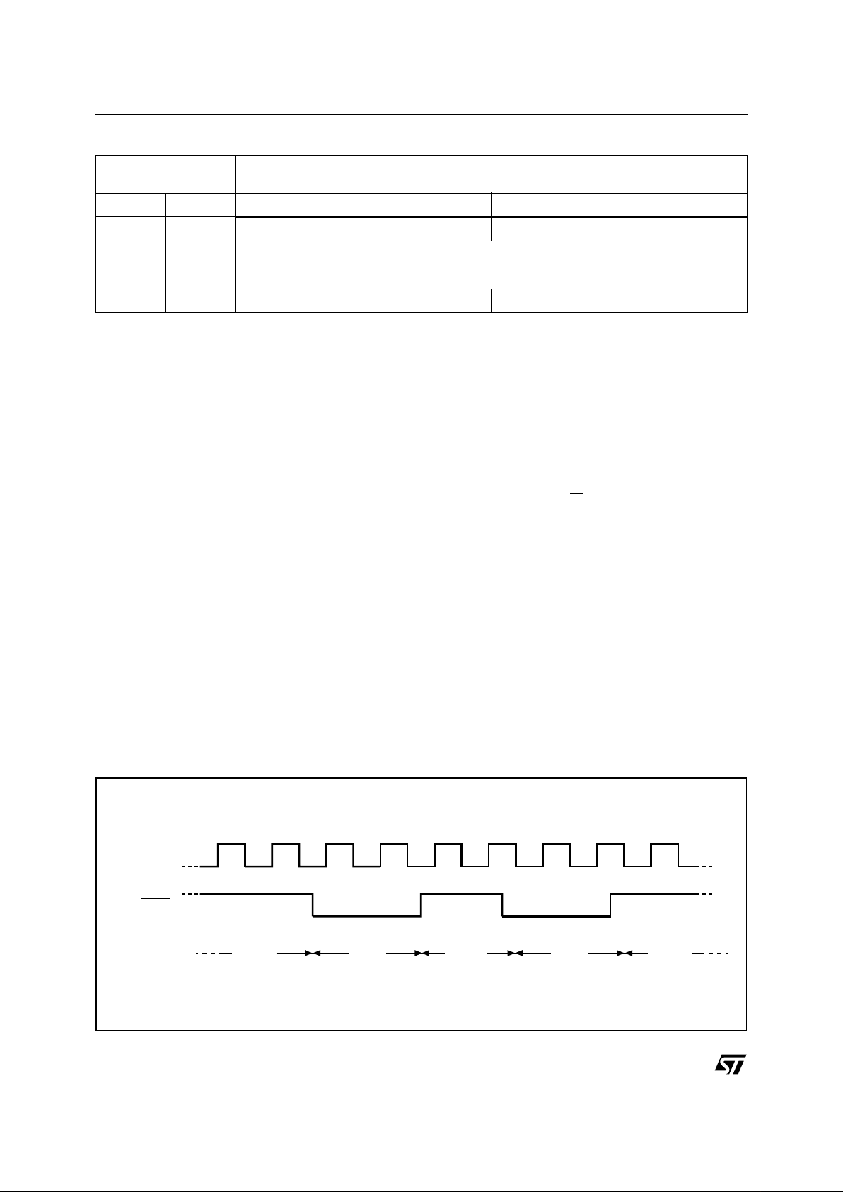
Figure 6. Hold Condition Activation
Status Register
Content
Memory Content
BP1 Bit BP0 Bit Protected Area Unprotected Area
0 0 none All sectors (Sectors 0 and 1)
0 1
No protection against Page Program (PP) and Sector Erase (SE)
All sectors (Sectors 0 and 1) protected against Bulk Erase (BE)
1 0
1 1 All sectors (Sectors 0 and 1) none
AI02029C
HOLD
C
Active Hold Active Hold Active
Page 7

7/32
M25P05
Hold Condition
The Hold (HOLD
) signal is used to pause any serial communications with the device without resetting the clocking sequence. However, taking this
signal Low does not terminate any Write Status
Register, Program or Erase cycle that is currently
in progress.
To enter the Hold condition, the device must be
selected , wit h Ch ip Select (S
) Low.
The Hold condition starts on the falling edge of the
Hold (HOLD
) signal, provided that this coincides
with Serial Clock (C) being L ow (as sh own i n F igure 6).
The Hold condition ends on the rising edge of the
Hold (HOLD
) signal, provided that this coincides
with Serial Clock (C) being Low.
If the falling edge does not coincide with Serial
Clock (C) being Low, the Hold condition starts
when Serial Clock (C) next goes Low. Similarly, if
the rising edge does not coincide with Serial Clock
(C) being Low, the Hold condition ends when Serial Clock (C) next goes Low. (This is shown in Figure 6).
During the Hold condition, the Serial Data Output
(Q) is high impedanc e, and Serial D ata Input (D)
and Serial Clock (C) are Don’t Care.
Normally, the device is kept selected, with Chip
Select (S
) driven Low, for the whole duration of the
Hold condition. This is to en sure that the state of
the internal logic remains unchanged from the moment of entering the Hold condition.
If Chip Select (S
) goes High while the device is in
the Hold condition, this has the effect of reset ting
the internal logic of the device. To restart communication with the device, it is necessary to drive
Hold (HOLD
) High, and then to drive Chip Select
(S
) Low. This prevents the device from going back
to the Hold condition.
Page 8
M25P05
8/32
MEMORY OR GANIZATION
The memory is organized as:
■ 65536 bytes (8 bits each)
■ 2 sectors (256 Kbits, 32768 bytes each)
■ 512 pages (128 bytes each).
Each page can be individually programmed (bits
are programmed from 1 to 0). The device is Sector
or Bulk Erasable (bits are erased from 0 to 1) but
not Page Erasable.
Table 3. Memory Organization
Figure 7. Block Diagram
Sector Address Range
1 08000h 0FFFFh
0 00000h 07FFFh
AI04039
HOLD
S
W
Control Logic
High Voltage
Generator
I/O Shift Register
Address Register
and Counter
128 Byte
Data Buffer
128 Bytes (Page Size)
X Decoder
Y Decoder
C
D
Q
Status
Register
00000h
08000h
0FFFFh
0007Fh
Page 9
9/32
M25P05
INSTRUCTIONS
All instructions, addresses and data are shifted in
and out of the device, most significant bit first.
Serial Data Input (D) is sampled on the first rising
edge of Serial Clock (C) after Chip Select (S
) is
driven Low. Then, the one-byte instruction code
must be shifted in to the device, most significant bit
first, on Serial Data Input (D), each bit being
latched on the rising edges of Serial Clock (C).
The instruction set is listed in Table 4.
Depending on the instruction, the one-byte in-
struction code is follo wed by address bytes, o r by
data bytes, or by both or none. Chip Select (S
)
must be driven High after the last bit of the instruction sequence has been shifted in.
At the end of a Page P rogram (PP), Se ctor Eras e
(SE), Bulk Erase (BE) or Write Status Register
(WRSR) instruction, Chip Select (S
) must be driven High exactly at a byte boundary, otherwise the
instruction is rejected, and is not executed. That is,
Chip Select (S
) must driven High when the number
of clock pulses after Chip Select (S
) being driven
Low is an exact multiple of eight.
All attempts to acc ess t he m em ory array du ring a
Write Status Register cycle, Program cycle or
Erase cycle are ignored, and the internal Write
Status Register cycle, Program cycle or Erase cycle continues unaffected.
Table 4. Instruction Set
Instruction Description One-byte Instruction Code
WREN Write Enable 0000 0110
WRDI Write Disable 0000 0100
RDSR Read Status Register 0000 0101
WRSR Write Status Register 0000 0001
READ Read Data Bytes 0000 0011
PP Page Program 0000 0010
SE Sector Erase 1101 1000
BE Bulk Erase 1100 0111
DP Deep Power-down 1011 1001
RES Release from Deep Power-down, and Read Electronic Signature 1010 1011
Page 10

M25P05
10/32
Figure 8. Write Enable (WREN) Sequence
Write Enable (WREN)
The Write Enable (WREN) instruction (Fig ure 8)
sets the Write Enable Latch (WEL) bit.
The Write Enable Latch (WEL) bit must be set prior to every Page Program (PP), Sector Erase
(SE), Bulk Erase (BE) and Write Status Register
(WRSR) instruction.
The Write Enable (WREN) instruction is entered
by driving Chip Select (S
) Low, sending the in-
struction code, and then driving Chip Select (S
)
High.
Figure 9. Write Disable (WRDI) Sequence
Write Disable (WRDI)
The Write Disable (WRDI) instruction (Figure 9)
resets the Write Enable Latch (WEL) bit.
The Write Disable (WRDI) instruction is entered by
driving Chip Select (S
) Low, sending the instruc-
tion code, and then driving Chip Select (S
) High.
The Write Enable Latch (WEL) bit is reset under
the following conditions:
– Power-up
– Write Disable (WRDI) instruction completion
– Write Status Register (WRSR) instruction com-
pletion
– Page Program (PP) instruction completion
– Sector Erase (SE) instruction completion
– Bulk Erase (BE) instruction completion
C
D
AI02281D
S
Q
21 34567
High Impedance
0
Instruction
C
D
AI03750C
S
Q
21 34567
High Impedance
0
Instruction
Page 11

11/32
M25P05
Figure 10. Read Status Register (RDSR) Sequence
Read Status Register (RDSR)
The Read Status Register (RDSR) instruction allows the Status Register to be read. The Status
Register may be read at any time, even while a
Program, Erase or Write Status Register cycle is in
progress. When one of these cycles is i n pr ogress,
it is recommended to check the Write In Progress
(WIP) bit before sending a new instruction to the
device. It is also possible to read the S tatus Register continuously, as shown in Figure 10.
Table 5. Status Register Format
Note: 1. SRWD, BP1 and BP0 are non-volatile read and write bits.
2. WEL and WIP are volatil e read-only bi ts (WEL is set and
reset by specific instructions; WIP is automatically set
and reset by the internal logic of the device).
The status and cont rol bits of t he Stat us Register
are as follows:
WIP bit. The Write In Process (WIP) bit indi cates
whether the memory is busy with a Write Status
Register, Program or Erase cycle. When set to 1,
such a cycle is in progress, when reset to 0 no
such cycle is in progres s.
WEL bit. Th e Write Enable Latch (WEL) bit indicates the status of the internal Write Enable Latch.
When set to 1 the internal Write Enable Latch is
set, when set to 0 t he i nte rnal W rite E nabl e Latch
is reset and no Write S tatus Reg ister, Pr ogram or
Erase instruction is accepted.
BP1, BP0 bits. The Block Protect (BP1, BP0) bits
are non-volatile. They define the size of the area to
be software protected against Program and Erase
instructions. These bits are written with the Write
Status Register (WRSR) instruction. When both of
the Block Protect (BP1, BP0) bits are set to 1, the
whole memory is protected against Page Program
(PP) and Sector Erase (SE) instructions. The Bulk
Erase (BE) instruction is executed if, and only if,
both Block Protect (BP1, BP0 ) bits are 0. This is
summarized in Table 2 . The Block Protect (BP1,
BP0) bits can be written provided that the Hardware Protected mode has not been set.
SRWD bit. The Status Register Write Disable
(SRWD) bit is operated in conjunction with the
Write Protect (W
) signal. The Status Register
Write Disable (SRWD) bit an d Write Protect (W
)
signal allow the device to be put in the Hardware
Protected mode (when t he Status Register Write
Disable (SRWD) bit is set to 1, and Write Protect
(W
) is driven Low). In this mode, the non-volatile
bits of the Status Register (SRWD, BP1, BP0) become read-only bits and the Write Status Register
(WRSR) instruction is no longer accepted for execution.
C
D
S
21 3456789101112131415
Instruction
0
AI02031C
Q
7 6543210
Status Register Out
High Impedance
MSB
7 6543210
Status Register Out
MSB
7
b7 b0
SRWD 0 0 0 BP1 BP0 WEL WIP
Page 12

M25P05
12/32
Figure 11. Write Status Register (WRSR) Sequence
Write Status Register (WRSR)
The Write Status Register (WRSR) instruction allows new values to be written to the Status Register. Before it can be accepted, a Write Enable
(WREN) instruction must previously have been executed. After the Write Enable (WREN) instruction
has been decoded and ex ecuted, the device sets
the Write Enable Latch (WEL).
The Write Status Register (WRSR) instruction is
entered by driving Chip Select (S
) Low, followed
by the instruction code and the data byte on Serial
Data Input (D).
The instruction sequence is shown in Figure 11.
The Write Status Register (WRSR) instruction has
no effect on b6, b5, b4, b1 and b0 of the Status
Register. b6, b5 and b4 are always read as 0.
Chip Select (S
) must be driven High after the
eighth bit of the d ata byte has been latched in. If
not, the Write Status Register (WRSR) i nstruction
is not executed. As soon as Chip Select (S
) is driv-
en High, the se lf-timed Wri te Status Regist er cycle
(whose duration is tW) is initiated. While the Write
Status Register cycle is in progress, the Status
Register may still be read to check the value of the
Write In Progress (WIP) bit. The Write In Progress
(WIP) bit is 1 during the self-timed Write Status
Register cycle, and is 0 wh en it is completed. At
some unspecifi ed time befor e the cycle i s completed, the Write Enable Latch (WEL) is reset.
The Write Status Register (WRSR) instruction allows the user to change the values of the Block
Protect (BP1, BP0) bits, to define the size of the
area that is to be trea ted as read-only, as defined
in Table 2. The Write Status Register (WRSR) instruction also allows the user to set or reset the
Status Register Write Disable (SRWD) bit in accordance with the Write Protect (W
) signal. The
Status Register Write Disable (SRWD) bit and
Write Protect (W
) signal allow the device to be put
in the Hardware Protected Mode (HPM). The Write
Status Register (WRSR) instruction is not executed once the Hardware P rotected Mode (HPM) is
entered.
C
D
AI02282C
S
Q
21 3456789101112131415
High Impedance
Instruction Status
Register In
0
765432 0
1
MSB
Page 13

13/32
M25P05
Table 6. Protection Modes
Note: 1. As def i ned by the va lu es in the Block Protect (BP1, BP0) bits o f the Status Reg i st er, as shown i n T able 2.
The protection features of t he de vic e are su mmarized in Table 6.
When the Status Register Write Disable (SRWD)
bit of the Status Register is 0 (its initial delivery
state), it is possible to write to the Status Register
provided that the Write Enable Latch (WEL) bit has
previously been set by a Write Enable (WREN) instruction, regardless of th e whether W rite Prote ct
(W
) is driven High or Low.
When the Status Register Write Disable (SRWD)
bit of the Status Register is set to 1, two cases
need to be considered, depending on the st ate of
Write Protect (W
):
– If Write Protect (W
) is driven High, it is possible
to write to the Status Register provided that the
Write Enable Latch (WEL) bit has previously
been set by a Write Enable (WREN) instruction.
– If Write Protect (W
) is driven Low, it is
not
pos-
sible to write to the Status Register
even
if the
Write Enable Latch (WEL) bit has previously
been set by a Write Enable (WREN) instruction.
(Attempts to write to the Status Register are rejected, and are not accepted for ex ecution). As
a consequence, all the data bytes in the memory area that are software protected (SPM) by the
Block Protect (BP1, BP0) bits of the Status Register, are also hardware protected against data
modification.
Regardless of the order of the two events, the
Hardware Protected Mode (HPM) can be entered:
– by setting the Status Register Write Disable
(SRWD) bit after driving Write Protect (W
) Low
– or by driving Write Protect (W
) Low after setting
the Status Register Write Disable (SRWD) bit.
The only way to exit the Hardware Protected Mode
(HPM) once entered is to pull Write Protect (W
)
High.
If Write Protect (W
) is permanently tied High, the
Hardware Protected Mode (HPM) can never be
activated, and only t he Software Protec ted Mode
(SPM), using the Block Protect (B P1, BP 0) bi ts of
the Status Register, can be used.
W
Signal
SRWD
Bit
Mode
Write Protection of the
Status Register
Memory Content
Protected Area
1
Unprotected Area
1
10
Software
Protected
(SPM)
Status Register is
Writable (if the WREN
instruction has set the
WEL bit)
The values in the BP1
and BP0 bits can be
changed
Protected against Page
Program and Sector
Erase
Ready to accept Page
Program and Sector
Erase instructions
00
11
01
Hardware
Protected
(HPM)
Status Register is
Hardware write protected
The values in the BP1
and BP0 bits cannot be
changed
Protected against Page
Program and Sector
Erase
Ready to accept Page
Program and Sector
Erase instructions
Page 14

M25P05
14/32
Figure 12. Read Data Bytes (READ) Sequence
Note: 1. Address bits A23 to A16 must be set to 00h.
Read Data Bytes (READ)
The device is f irst s el ected b y dri ving Chip S ele ct
(S
) Low. The instruction code for the Read Data
Bytes (READ) instruction is followed by a 3-byte
address (A23-A0), each bit being latched-in during
the rising edge of Serial Clock (C). Then the memory contents, at that address, is shifted out on Serial Data Output (Q), each bit being shifted o ut, at
a maximum frequency f
R
, during the falling edge of
Serial Clock (C).
The instruction sequence is shown in Figure 12.
The first byte addressed can be at any location.
The address is automatically incremented to the
next higher address after each byte of data is shifted out. The whole memory can, therefore, be read
with a single Read Data Bytes (READ) i nst ruction.
There is no address roll-over; when the highest
address (0FFFFh) is reached, the instruction
should be terminated.
The Read Data Bytes (READ) instruction is terminated by driving Chip Select (S
) High. Chip Select
(S
) can be driven High at any time during data output. Any Read Data Bytes (READ) instruction,
while an Erase, Program or Write cycle is in
progress, is rejected without having any effects on
the cycle that is in progr es s.
C
D
AI03748C
S
Q
23
21 345678910 2829303132333435
2221 3210
36 37 38
76543 1 7
0
High Impedance
Data Out 1
Instruction 24-Bit Address
0
MSB
MSB
2
39
Data Out 2
Page 15

15/32
M25P05
Figure 13. Page Program (PP) Sequence
Note: 1. Address bits A23 to A16 must be set to 00h.
Page Program (PP)
The Page Program (PP) instruction allows bytes to
be programmed in the memory (changing bits from
1 to 0). Before it can be accept ed, a Wri te Enab le
(WREN) instruction must previously have been executed. After the Write Enable (WREN) instruction
has been decoded, the device sets the Write Enable Latch (WEL).
The Page Program (PP) instruction is entered by
driving Chip Select (S
) Low, followed by the instruction code, three address b ytes (of which the
most significant byte, A23-A16, must be 00h) and
at least one data byte on Serial Data Input (D). If
the 7 least significant address bits (A6-A0) are not
all zero, all transmitted data exceeding the addressed page boundary roll over, and are programmed from the start address of the same page
(the one whose 7 least significant address bits
(A6-A0) are all zero). Chip Select (S
) must be driv-
en Low for the entire duration of the sequence.
The instruction sequence is shown in Figure 13.
If more than 128 bytes are sent to the device, pre-
viously latched data are discarded and the last 128
data bytes are guaranteed to be programmed correctly within the same page. If less than 128 Data
bytes are sent to device, they are correctly programmed at the requested addresses without having any effects on the other bytes of the same
page.
Chip Select (S
) must be driven High after the
eighth bit of the last data byte has been latched in,
otherwise the Page Program (PP) instruction is not
executed.
As soon as Chip Select (S
) is driv en Hi g h , t h e se lf -
timed Page Program cycle (whose duratio n i s t
PP
)
is initiated. While the Page Program cycle is in
progress, the Status Register may be read to
check the value of the Write In Progress (WIP) bit.
The Write In Progress (WIP) bit is 1 during the selftimed Page Program cycle, and is 0 when it is
completed. When th e cycle is com pleted, the Wri te
Enable Latch (WEL) bit is reset.
A Page Program (PP) instruction applied to a page
which is protected by the Block Protect (BP0, BP1)
bits (see Table 2) is not executed.
C
D
AI03749C
S
4241 43 44 45 46 47 48 49 50 52 53 54 5540
C
D
S
23
21 345678910 2829303132333435
2221 3210
36 37 38
Instruction 24-Bit Address
0
765432 0
1
Data Byte 1
39
51
765432 0
1
Data Byte 2
765432 0
1
Data Byte 3 Data Byte 128
1055
1054
1053
1052
1051
1050
1049
765432 0
1
1048
MSB
MSB
MSB MSB MSB
Page 16

M25P05
16/32
Figure 14. Sector Erase (SE) Sequence
Note: 1. Address bits A23 to A16 must be set to 00h.
Sector Erase (SE)
The Sector Erase (SE) instruction sets t o 1 (FFh)
all bits inside the chosen sector. Bef ore it can be
accepted, a Write Enable (WREN) instruction
must previously have been executed. After the
Write Enable (WREN) instruction has been decoded, the device sets the Write Enable Latch (WEL).
The Sector Erase (SE) instruction is entered by
driving Chip Select (S
) Low, followed by the instruction code, and three address by tes on Serial
Data Input (D). Any address inside the Sector (see
Table 3) is a valid address for the Sector Erase
(SE) instruction. Chip Select (S
) must be driven
Low for the entire duration of the sequence.
The instruction sequence is shown in Figure 14.
Chip Select (S
) must be driven High after the
eighth bit of the last address byte has been latched
in, otherwise the S ector Erase (SE) i nstruction is
not executed. As soon as Chip Select (S
) is driven
High, the self -timed Sector E rase cycle (who se duration is t
SE
) is initiated. While the Sector Erase cycle is in progress, the Status Register may be read
to check the value of the Write In Progress (WIP)
bit. The Write In Progress (WIP) bit is 1 during the
self-timed Sector Erase cycle, and is 0 when it is
completed. At some unspecified time before the
cycle is completed, the Write Enable Latch (WEL)
bit is reset.
A Sector Erase (S E) in struction applie d t o a page
which is protected by the Block Protect (BP1, BP0)
bits (see Table 2) is not executed.
24 Bit Address
C
D
AI03751C
S
21 3456789 293031
Instruction
0
23 22 2 0
1
MSB
Page 17

17/32
M25P05
Figure 15. Bulk Erase (BE) Sequence
Bulk Erase (B E)
The Bulk Erase (BE) instruction sets all bits to 1
(FFh). Before it can be ac cepted, a Write Enable
(WREN) instruction must previously have been executed. After the Write Enable (WREN) instruction
has been decoded, the device sets the Write Enable Latch (WEL).
The Bulk Erase (BE) instruction is entered by driving Chip Select (S
) Low, followed by the instruction
code on Serial Data Input (D). Chip Select (S
)
must be driven Low for the entire duration of the
sequence.
The instruction sequence is shown in Figure 15.
Chip Select (S
) must be driven High after the
eighth bit of the instruction code has been latched
in, otherwise the Bulk Erase instruction is not executed. As soon as Chip Select (S
) is driven High,
the self-ti med Bu l k Era se cycl e (who se duration is
t
BE
) is initiated. While the Bulk Erase cycle is in
progress, the Status Register may be read to
check the value of the Write In Progress (WIP) bit.
The Write In Progress (WIP) bit is 1 during the selftimed Bulk Erase cycle, a nd is 0 when it is completed. At some unspecified time before the cycle
is completed, the Write Enable Latch (WEL) bit is
reset.
The Bulk Erase (BE) instruction is executed only if
both Block Protect (BP1, BP0) bits are 0. The Bulk
Erase (BE) instruction is ignored if one, or more,
sectors are protected.
C
D
AI03752C
S
21 345670
Instruction
Page 18

M25P05
18/32
Figure 16. Deep Power-down (DP) Sequence
Deep Power-down (DP)
Executing the Deep Power-down (DP) instruction
is the only way to put the device in the lowest consumption mode (the Deep Power-down mode). It
can also be used as an extra s oftware protection
mechanism, while the device is not in active use,
since in this mod e, the device ign ores all Write,
Program and Erase instructions.
Driving Chip Select (S
) High deselects the device,
and puts the device in the S tandby m ode (if there
is no internal cycle currently in progress). But this
mode is not the Deep Power-down mode. The
Deep Power-down mode can only b e entered by
executing the Deep Power-down (DP ) instruction,
to reduce the standby current (from I
CC1
to I
CC2
,
as specified in Table 13).
Once the device has entered the Deep Power-
down mode, all instructions are ignored except the
Release from Deep Power-down and Read Electronic Signature (RES) instruction. This releases
the device from this mode. The Release from
Deep Power-down and Read Electronic Signature
(RES) instruction also allows the Electronic Signa-
ture of the device to be output on Serial Data Output (Q).
The Deep Power-down m ode automatically stops
at Power-down, and the device always Powers-up
in the Standby mode.
The Deep Power-down (DP) instruction is entered
by driving Chip Select (S
) Low, followed by the instruction code on Serial Da ta Input (D). Chip Select (S
) must be driven Low for the entire duration
of the sequence.
The instruction sequence is shown in Figure 16.
Chip Select (S
) must be driven High after the
eighth bit of the instruction code has been latched
in, otherwise the Deep Power-down (DP) instruction is not executed. As soon as Chip Select (S
) is
driven High, it requires a delay of t
DP
before the
supply current is reduced to I
CC2
and the Deep
Power-down mode is entered.
Any Deep Power-down (DP) instruction, while an
Erase, Program or Write cycle is in progress, is rejected without havi ng any effects on the cycle that
is in progress.
C
D
AI03753C
S
21 345670
t
DP
Deep Power-down Mode
Stand-by Mode
Instruction
Page 19

19/32
M25P05
Figure 17. Release from Deep Power-d ow n and Read Electronic Sign atur e (RES) Sequen ce
Release from Deep Power-down and Read
Electronic Signature (RES)
Once the device has entered the Deep Powerdown mode, all instructions are ignored except the
Release from Deep Power-down and Read Electronic Signature (RES) instruction. Executing this
instruction takes the device out of the Deep Power-down mode. The instruction can also be used to
read, on Serial Data Output (Q), the 8-bit Electronic Signature of the device.
Except while an Erase, P rogram or Write Status
Register cycle is in progress, the Release from
Deep Power-down and Read Electronic Signature
(RES) instruction always provides access to the
Electronic Signature of the device, and can be applied even if the Deep Power-down mode has not
been entered.
Any Release from Deep Power-down and Read
Electronic Signature (RES) instruction while an
Erase, Program or Write Status Register cycle is in
progress, is not decoded, and has no effect on the
cycle that is in progress.
This instruction serves a second purpose. The device features an 8-bit Electronic Signature, whose
value for the M25P05 is 10h. This can be read using the Release from Deep Power-down and Read
Electronic Signature (RES) instruction.
The device is f irst s el ected b y dri ving Chip S el ect
(S
) Low. The instruction code is followed by a
dummy 3-byte a ddress (A23-A0), each bit be ing
latched-in on Serial Data Input (D) during the rising
edge of Serial Clock (C). Then, the 8-bit Electronic
Signature, stored in t he m emo ry, i s shifte d ou t on
Serial Data Output (Q), each bit being shifted out
during the falling edge of Serial Clock (C).
The instruction sequence is shown in Figure 17.
The Release from Deep Power-down and Read
Electronic Signature (RES) instruction is terminated by driving Chip Sele ct (S
) High after the Electronic Signature has been read at least once.
Sending additional clock cycles on Serial Clock
(C), while Chip Select (S
) is driven Low, cause the
Electronic Signature to be output repeatedly.
Once Chip S elect (S
) is driven High, the device is
put in the Standby mode. Th e device waits to be
selected, so that it can rec eive, decode an d execute instructions.
C
D
AI03755C
S
Q
23
21 345678910 2829303132333435
2221 3210
36 37 38
765432 0
1
High Impedance
Electronic Signature Out
Instruction 24-Bit Address
0
MSB
Stand-by Mode
Deep Power-down Mode
MSB
Page 20

M25P05
20/32
Figure 18. Release from Deep Power-dow n (RES) Sequence
Driving Chip Select (S
) High after the 8-bit instruction byte has been received by the device, but before the whole of the 8-bit Electronic Signature has
been transmitted for the first time (as shown in Fig-
ure 18), still insures that the device is taken out of
the Deep Power-down mode, but incurs a delay
(t
RES
) before the device is pu t in Standby mode.
Chip Select (S
) must remain High for at least
t
RES
(max), as specified in Table 14.
C
D
AI03754C
S
21 345670
t
RES
Stand-by Mode
Deep Power-down Mode
Q
High Impedance
Instruction
Page 21

21/32
M25P05
POWER-UP, POWER-DOWN AND DELIVERY STATE
Power-up
At Power-up, the device must not be selected (that
is Chip Se lect (S
) must follow the voltage supplied
on V
CC
) until the supply voltage reaches
V
CC
(min), and a further t
VSL
delay has elapsed.
To avoid data corruption and inadvertent write
operations during power up, a Power On Reset
(POR) circuit is included. The logic inside the
device is held reset while V
CC
is less than the POR
threshold value, V
WI
– all operations are disabled,
and the device will not respo nd to any instruction.
Similarly, when V
CC
drops from the operating
voltage, to below the POR threshold value, V
WI
, all
operations are disabled and the device will not
respond to any instruction.
No instructions (including Read, Write Status
Register, Program or Erase instructions) should
be sent to the device until a time delay of t
VSL
after
V
CC
has risen above the VCC(min) level.
Moreover, the device ignores all Page Program
(PP), Sector Erase (SE), Bulk Erase (BE) and
Write Status Register (WRSR) instructions until a
time delay of t
PUW
has elapsed aft er the moment
that V
CC
rises above the VWI threshold. However,
the correct operation of the device is not
guaranteed if, by this time, V
CC
is still below
V
CC
(min). No Write Status Register, Program or
Erase instructions should be sent until the later of:
–t
PUW
after VCC passed the VWI threshold
–t
VSL
afterVCC passed the VCC(min) level
These values are specified in Table 7.
At Power-up, the device is in the following state:
– The device is in the Standby mode (not the
Deep Power-down mode).
– The Write Enable Latch (WEL) bit is reset.
Figure 19. Power-up Timing
Table 7. Power-Up Timing and V
WI
Threshol d
Note: 1. These parameters are characterize d onl y.
Symbol Parameter Min. Max. Unit
t
VSL
1
VCC(min) to S low
10 µs
t
PUW
1
Time delay to Write instruction 15 ms
V
WI
1
Write Inhibit Voltage 1.5 2.5 V
V
CC
AI04009B
VCC(min)
V
WI
Reset State
of the
Device
Chip Selection Not Allowed
Program, Erase and Write Commands are Rejected by the Device
tVSL
tPUW
time
Read Access allowed Device fully
accessible
Page 22

M25P05
22/32
Power-down
At Power-up and Power-down, the device must
not be selected (that is Chip Select (S
) must follow
the voltage applied on V
CC
) until VCC reaches the
correct value:
–V
CC
(min) at Power-up
–V
SS
at Power-down
A simple pull-up resistor on Chip Select (S
) can be
used to insure safe and proper Power-up and
Power-down.
INITIAL DELIVERY STATE
The device is delivered with the memory array
erased: all bits are set to 1 (each byte contains
FFh). The Status Register contains 00h (all Status
Register bits are 0).
Table 8. Initial Status Register Format
b7 b0
0 0000000
Page 23

23/32
M25P05
MAXIMUM RATIN G
Stressing the device ab ove the rating listed in t he
Absolute Maximum Ratings" table may cause permanent damage to the device. These are stress
ratings only and operation of the device at these or
any other conditions ab ove those i ndicated in t he
Operating sections of this specificat ion is not im-
plied. Exposure to Absolute Maximum Rating conditions for extended periods may affect device
reliability. Refer also to the STMicroelectronics
SURE Program and ot her relevant quality documents.
Table 9. Absolute Maximum Ratings
Note: 1. IPC/JED EC J- STD- 020 A
2. JEDEC Std JESD22-A114A (C1=100 pF, R1=1500 Ω, R2=500 Ω)
Symbol Parameter Min. Max. Unit
T
STG
Storage Temperature –65 150 °C
T
LEAD
Lead Temperature during Soldering (20 seconds max.)
1
235 °C
V
IO
Input and Output Voltage (with respect to Ground) –0.6 4.0 V
V
CC
Supply Voltage –0.6 4.0 V
V
ESD Electrostatic Discharge Voltage (Human Body model)
2
–2000 2000 V
Page 24

M25P05
24/32
DC AND AC PARAMETERS
This section summarizes the operat ing and measurement conditions, and the DC and AC characteristics of the device. The parameters in t he DC
and AC Characteristic tables that follow are derived from tests performed under the Measure-
ment Conditions summarized in the relevant
tables. Designers should chec k th at the o perat ing
conditions in their circuit matc h the meas urement
conditions when relying on the quoted parameters.
Table 10. Operating Conditions
Table 11. AC Measurement Conditions
Note: 1. Output Hi-Z is defin ed as the point w here data out is no l onger driven.
Figure 20. AC Measurement I/O Waveform
Table 12. Capacitance
Note: Sampl ed only, not 10 0% tested, at TA=25°C an d a frequency of 20 MHz.
Symbol Parameter Min. Max. Unit
V
CC
Supply Voltage 2.7 3.6 V
T
A
Ambient Operating Temperature –40 85 °C
Symbol Parameter Min. Max. Unit
C
L
Load Capacitance 30 pF
Input Rise and Fall Times 5 ns
Input Pulse Voltages
0.2V
CC
to 0.8V
CC
V
Input and Output Timing Reference Voltages
0.3V
CC
to 0.7V
CC
V
AI00825
0.8V
CC
0.2V
CC
0.7V
CC
0.3V
CC
Symbol Parameter Test Condition Min. Max. Unit
C
OUT
Output Capacitance (Q) V
OUT
= 0V 8 pF
C
IN
Input Capacitance (other pins) VIN = 0V 6 pF
Page 25

25/32
M25P05
Table 13. DC Characteristics
Symbol Parameter
Test Condition
(in addition to those in Table 10)
Min. Max. Unit
I
LI
Input Leakage Curren t ± 2 µA
I
LO
Output Leakage Current ± 2 µA
I
CC1
Standby Current
S
= VCC, V
IN
= VSS or V
CC
50 µA
I
CC2
Deep Power-down Current S = VCC, V
IN
= VSS or V
CC
5µA
I
CC3
Operating Current (READ)
C = 0.1V
CC
/ 0.9.VCC at 20 MHz,
Q = open
3mA
I
CC4
Operating Current (PP) S = V
CC
15 mA
I
CC5
Operating Current (WRSR) S = V
CC
15 mA
I
CC6
Operating Current (SE) S = V
CC
15 mA
I
CC7
Operating Current (BE)
S
= V
CC
15 mA
V
IL
Input Low Voltage – 0.5
0.3V
CC
V
V
IH
Input High Voltage
0.7V
CC
VCC+1
V
V
OL
Output Low Voltage IOL = 1.6 mA 0.4 V
V
OH
Output High Voltage
I
OH
= –100µAV
CC
–0.2
V
Page 26

M25P05
26/32
Table 14. AC Characteristics
Note: 1. tCH + tCL must be greater than or equal to 1/ f
C
2. Value guar anteed by characteriza tion, not 100% tested in pro duction.
Test conditions specified in Table 10 and Table 11
Symbol Alt. Parameter Min. Max. Unit
f
C
f
C
Clock Frequency D.C. 2 0 MHz
t
SLCH
t
CSS
S Active Setup Time (relative to C) 10 ns
t
CHSL
S Not Active Hold Time (relative to C) 10 ns
t
CH
1
t
CLH
Clock High Time 22 ns
t
CL
1
t
CLL
Clock Low Time 22 ns
t
DVCH
t
DSU
Data In Setup Time 5 ns
t
CHDX
t
DH
Data In Hold Time 5 ns
t
CHSH
S Active Hold Time (relative to C) 10 ns
t
SHCH
S Not Active Setup Time (relative to C) 10 ns
t
SHSL
t
CSH
S Deselect Time 50 ns
t
SHQZ
2
t
DIS
Output Disable Time 20 ns
t
CLQV
t
V
Clock Low to Output Valid 20 ns
t
CLQX
t
HO
Output Hold Time 0 ns
t
HLCH
HOLD Setup Time (relative to C) 10 ns
t
CHHH
HOLD Hold Time (relative to C) 10 ns
t
HHCH
HOLD Setup Time (relative to C) 10 ns
t
CHHL
HOLD Hold Time (relative to C) 10 ns
t
HHQX
2
t
LZ
HOLD to Output Low-Z 20 ns
t
HLQZ
2
t
HZ
HOLD to Output High-Z 20 ns
t
DP
2
S High to Deep Power-down Mode 1.6
µ
s
t
RES
2
S High to Standby Mode 1.6
µ
s
t
W
Write Status Register Cycle Time 5 ms
t
PP
Page Program Cycle Time 5 ms
t
SE
Sector Erase Cycle Time 2 s
t
BE
Bulk Erase Cycle Time 4 s
Page 27

27/32
M25P05
Figure 21. Serial Input Timing
Figure 22. Hold Timi ng
C
D
AI01447C
S
MSB IN
Q
tDVCH
High Impedance
LSB IN
tSLCH
tCHDX
tCHCL
tCLCH
tSHCH
tSHSL
tCHSHtCHSL
C
Q
AI02032
S
D
HOLD
tCHHL
tHLCH
tHHCH
tCHHH
tHHQXtHLQZ
Page 28

M25P05
28/32
Figure 23. Output Timing
C
Q
AI01449C
S
LSB OUT
D
ADDR.LSB IN
tSHQZ
tCH
tCL
tQLQH
tQHQL
tCLQX
tCLQV
Page 29

29/32
M25P05
PACKAGE MECHANICAL
SO8 narrow – 8 lead Plastic Small Outline, 150 mils body width
Note: Drawing is not to scale.
SO8 narrow – 8 lead Plastic Small Outline, 150 mils body width
SO-a
E
N
CP
B
e
A
D
C
LA1 α
1
H
h x 45˚
Symb.
mm inches
Typ. Min. Max. Typ. Min. Max.
A 1.35 1.75 0.053 0.069
A1 0.10 0.25 0.004 0.010
B 0.33 0.51 0.013 0.020
C 0.19 0.25 0.007 0.010
D 4.80 5.00 0.189 0.197
E 3.80 4.00 0.150 0.157
e 1.27 – – 0.050 – –
H 5.80 6.20 0.228 0.244
h 0.25 0.50 0.010 0.020
L 0.40 0.90 0.016 0.035
α
0° 8° 0° 8°
N8 8
CP 0.10 0.004
Page 30

M25P05
30/32
PART NUMBERING
Table 15. Ordering Information Scheme
For a list of available options (speed, package,
etc.) or for further information on any aspect of this
device, please contact your nearest ST Sales O ffice.
Example: M25P05 –VMN6T
Device Type
M25P
Device Function
05 = 512 Kbit (64K x 8)
Operating Voltage
V = V
CC
= 2.7 to 3.6V
Package
MN = SO8 (150 mil width)
Temperature Range
6 = –40 to 85 °C
Option
T = Tape & Reel Packing
Page 31

31/32
M25P05
REVISION HIST ORY
Table 16. Document Revision History
Date Description of Revision
09-Feb-2001 1.0 Document written
26-Mar-2001 1.1 Correction to descriptions on Hold condition and Power up: no parameters changed
12-Apr-2001 1.2 Descriptions of Page Programming made more precise
25-May-2001 1.3 Serial Paged Flash Memory renamed as Serial Flash Memory
11-Sep-2001 1.4
Changes to text: Signal Description/Chip Select; Hold Condition/1st para; Protection modes;
Release from Power-down and Read Electronic Signature (RES); Power-up
Repositioning of several tables and illustrations without changing their contents
Power-up timing illustration; SO8W package removed
Changes to tables: Abs Max Ratings/V
IO
; DC Characteristics/V
IL
25-Feb-2002 1.5 Product is “Not for New Design”
Page 32

M25P05
32/32
Information furnished is believed to be accurate and reliable. However, STMicroelectronics assumes no responsibility for the consequences
of use of such information nor for any infringement of patents or other rights of third parties which may result from its use. No license is granted
by implic ation or otherwise under any patent or p atent rights of STMi croelectr oni cs. Spec i fications mentioned i n this publicatio n are subject
to change without notice. This publication supersedes and replaces all information previously supplied. STMicroelectronics products are not
authorized for use as cri tical comp onents in life support dev i ces or systems wi t hout expres s written approval of STMi croelectr o nics.
The ST logo is registered trademark of STMicroelectronics
All other names are the propert y of their respective owners
© 2002 STMicroelectronics - All Rights Reserved
STMicroel ectronics group of companies Australia - Brazil - Canada - China - Finland - France - Germany - Hong Kon g -
India - Israel - Italy - Japan - Malaysia - Malta - Morocco - Singapore - Spain - Sweden - Switzerland - United Kingdom - United States.
www.st.com
 Loading...