

Page 1
M24C64
M24C32
64Kbit and 32Kbit Serial I²C Bus EEPROM
FEATURES SUMMARY
■ Two Wire I
Supports 400 kHz Protocol
■ Single Supply Voltage:
– 4.5V to 5.5V for M24Cxx
– 2.5V to 5.5V for M24Cxx-W
– 1.8V to 5.5V for M24Cxx-R
■ Write Control Input
■ BYTE and PAGE WRITE (up to 32 Bytes)
■ RANDOM and SEQUENTIAL READ Modes
■ Self-Tim e d P rogramming Cycle
■ Automatic Address Incrementing
■ Enhanced ESD/Latch-Up Behavior
■ More than 1 Million Erase/Write Cycles
■ More than 40 Year Data Retention
2
C Serial Interface
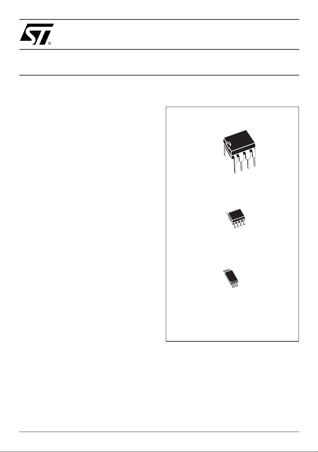
Figure 1. Packages
8
1
PDIP8 (BN)
8
1
SO8 (MN)
150 mil width
TSSOP8 (DW)
169 mil width
1/24May 2003
Page 2
M24C64, M24C32
SUMMARY DESCRIPTION
2
These I
C-compatible electrically erasable
programmable memory (EEPROM) devices are
organized as 8192 x 8 bits (M24C64) and 4096 x 8
bits (M24C32).
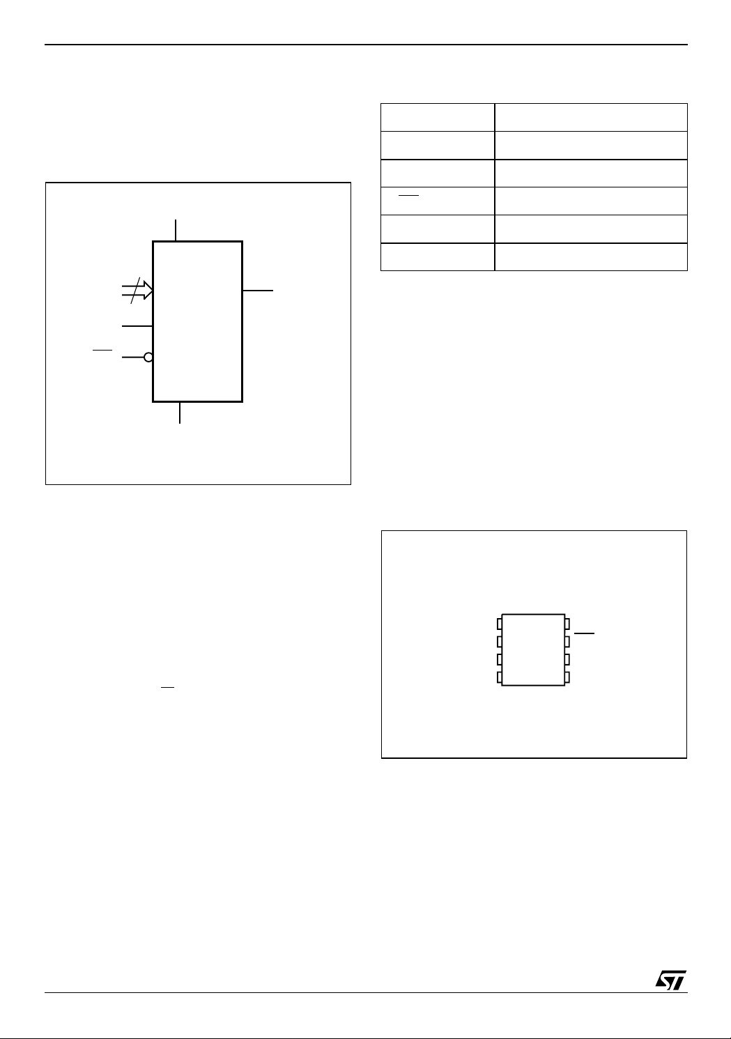
Figure 2. Logic Diagram
V
CC
3
E0-E2 SDA
SCL
WC
M24C64
M24C32
V
SS
AI01844B
Table 1. Signal Names
E0, E1, E2 Chip Enable
SDA Serial Data
SCL Serial Clock
WC
V
CC
V
SS
Power On Reset: V
Write Control
Supply Voltage
Ground
Lock-Out Write Protect
CC
In order to prevent data corruption and inadvertent
Write operations during Power-up, a Power On
Reset (POR) circuit is included. The internal reset
is held active until V
has reached the POR
CC
threshold value, and all operations are disabled –
the device will not respond to any command. In the
same way, when V
drops from the operating
CC
voltage, below the POR threshold value, all operations are disabled and the device will not respond
to any command. A stable and valid V
must be
CC
applied before applying any logic signal.
These devices are compatible with the I
2
C memory protocol. This is a two wire s erial interface that
uses a bi-directional data bus and serial clock. The
devices carry a built-in 4-bit Device Type Identifier
code (1010) in accordance with the I
2
C bus defini-
tion.
The device behaves as a slave in the I
2
C protocol,
with all memory operations synchronized by the
serial clock. Read and Write operations are initiated by a Start condition, generated by the bus master. The Start condition is followed by a Device
Select Code and RW
bit (as described in Table 2),
terminated by an acknowledge bit.
When writing data to the memory, the device in-
serts an acknowledge bit during the 9
th
bit time,
following the bus master’s 8-bit transmission.
When data is read by the bus master, the bus
master acknowledges the receipt of the data byte
in the same way. Data transfers are terminated by
a Stop condition after an Ack for Write, and after a
NoAck for Read.
Figure 3. DIP, SO and TSSOP Connections
M24C64
M24C32
1
E0 V
2
3
E2
4
SS
Note: 1. See page 19 (onwards) for package dimensions, and how
to identify pin-1.
8
7
6
5
AI01845C
CC
WCE1
SCL
SDAV
2/24
Page 3
SIGNAL DESCRIPTION
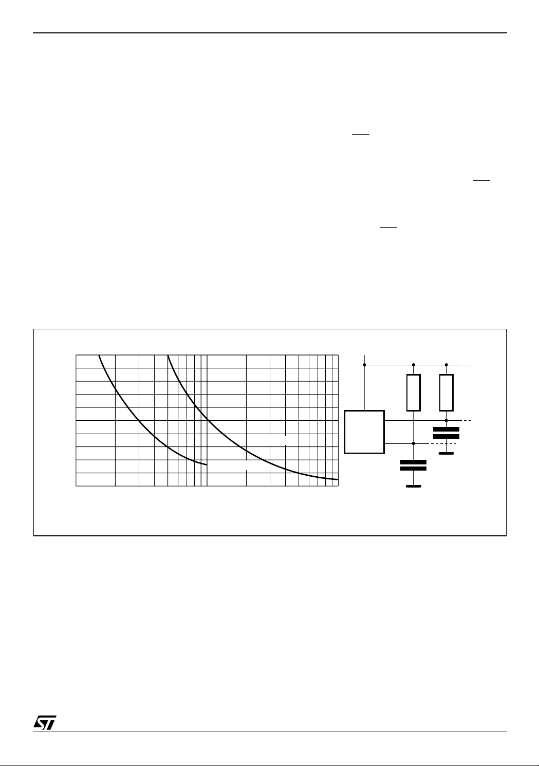
Serial Clock (SCL)
This input signal is used to strobe all data in and
out of the device. In applications where this signal
is used by slave devices to synchronize the bus to
a slower clock, the bus master must have an open
drain output, and a pull-up resistor must be connected from Serial Clock (SCL) to V
. (Figure 4
CC
indicates how the value of the pull-up resist or can
be calculated). In most applications, thoug h, this
method of synchronization is no t employed, and
so the pull-up resistor is not necessary, provided
that the bus maste r has a push-pull (rather than
open drain) output.
Serial Data (SDA)
This bi-directional signal is used to transfer data in
or out of the device. It is an open drain output that
may be wire-OR’ed with other open drain or open
collector signals on the bus. A pull up resistor must
be connected from Serial Data (SDA) to V
CC
. (Figure 4 indicates how the value of the pull-up resistor
can be calculated).
M24C64, M24C32
Chip Enable (E0, E1, E2)
These input signals are used to set the value that
is to be looked for on the three least significant bits
(b3, b2, b1) of the 7-bit Device Select Code. These
inputs must be tied to V
Device Select Code.
Write Control (WC
This input signal is useful for protecting the entire
contents of the memory from inadvertent write operations. Write operations are disabled to the entire memory array when Write Control (WC
driven High. When unconnected, the signal is internally read as V
IL
lowed.
When Write Control (WC
Select and Address bytes are acknowledged,
Data bytes are not acknowledged.
or VSS, to establish the
CC
)
) is
, and Write operations are al-
) is driven High, Device
Figure 4. Maximum R
20
16
12
8
Maximum RP value (kΩ)
4
0
10 1000
Value versus Bus Capacitance (C
L
fc = 100kHz
fc = 400kHz
100
C
(pF)
BUS
) for an I2C Bus
BUS
MASTER
V
CC
R
SDA
SCL
R
C
BUS
L
C
BUS
AI01665
L
3/24
Page 4
M24C64, M24C32
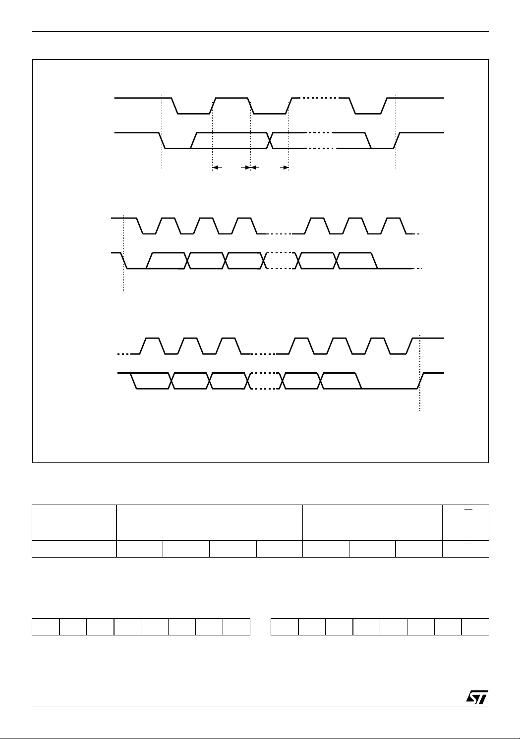
Figure 5. I2C Bus Protocol
SCL
SDA
SCL
SDA
SCL
SDA
START
Condition
START
Condition
1 23 789
MSB
1 23 789
MSB ACK
SDA
Input
SDA
Change
STOP
Condition
ACK
STOP
Condition
AI00792B
Table 2. Device Select Code
Device Type Identifier
1
Chip Enable Address
b7 b6 b5 b4 b3 b2 b1 b0
Device Select Code 1 0 1 0 E2 E1 E0 RW
Note: 1. The most si gnifican t bit, b7, is se nt first.
2. E0 , E 1 and E2 are compared agai nst the respective external pins on the memory device.
2
RW
Table 3. Most Significant Byte Table 4. Least Significant Byte
b15 b14 b13 b12 b11 b10 b9 b8 b7 b6 b5 b4 b3 b2 b1 b0
4/24
Page 5
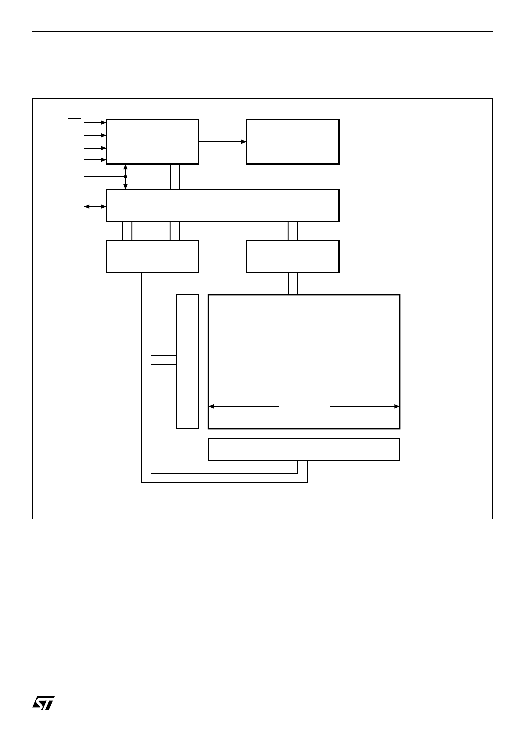
MEMORY ORGANIZATI ON
The memory is organized as shown in Figure 6.
Figure 6. Block Diagram
WC
E0
E1
E2
SCL
Control Logic
M24C64, M24C32
High Voltage
Generator
SDA
Address Register
and Counter
I/O Shift Register
Data
Register
Y Decoder
1 Page
X Decoder
AI06899
5/24
Page 6
M24C64, M24C32
DEVICE OPERATION
2
The device supports the I
C proto col. This is su m marized in Figure 5. Any device that sends data on
to the bus is defined to be a transmitter, a nd any
device that reads the data to be a receiver. The
device that controls the data transfer is known as
the bus master, and the other as the slave device.
A data transfer can only be initiated by the bus
master, w h ic h will als o provid e t h e s e r i a l c lo c k f or
synchronization. The M24Cxx device is always a
slave in all communication.
Start Condition
Start is identified by a falling edge of Serial Data
(SDA) while Serial Clock (SCL) is stable in the
High state. A Start condition must precede any
data transfer command. The devi ce continuously
monitors (except duri ng a Write cycle ) Se ri a l Data
(SDA) and Serial Clock (SCL) for a Start condition,
and will not respond unless one is give n.
Stop Condition
Stop is identified by a rising edg e of Serial Data
(SDA) while Serial Clock (SCL) is stable and driven High. A Stop condition terminates communication between the device and the bus master. A
Read command that is followed by NoAck can be
followed by a Stop condi tion to force the device
into the Stand-by mode. A Stop condition at the
end of a Write command triggers the internal EEPROM Wr ite cyc le.
Acknowledge Bit (ACK)
The acknowledge bit is used to indicate a successful byte transfer. The bus transmitter, whether it be
bus master or slave device, releases Serial Data
(SDA) after sending eight bits of data. During the
th
clock pulse period, the receiver pulls Serial
9
Data (SDA) Low to acknowledge the receipt of the
eight data bits.
Data Input
During data input, the device samples Serial Data
(SDA) on the rising edge of Serial Clock (SCL).
For correct device operation, Serial Data (SDA)
must be stable during the rising edge of Serial
Clock (SCL), and the Serial Data (SDA) signal
only
must change
when Serial Clock (SCL) is driv-
en Low.
Memory Addressing
To start communication betwee n the bus master
and the slave device, the bus mas ter mus t initiate
a Start condition. Following this, t he bus master
sends the Device Select Code, shown in Tabl e 2
(on Serial Data (SDA), most significant bit first).
The Device Select Code consists of a 4-bit Device
Type Identifier, and a 3-bit Chip Enable “Address”
(E2, E1, E0). To address the memory array, t he 4bit Device Type Identifier is 1010b.
Up to eight memory devices can be connected on
a single I
2
C bus. Each one is given a uniq ue 3-bit
code on the Chip Enable (E0, E1, E2) inputs.
When the Device Select Code is received on Serial Data (SDA), the device only responds if the Chip
Enable Address is the same as the value on the
Chip Enable (E0, E1, E2) inputs.
th
The 8
bit is the Read/Write bit (RW). This bi t is
set to 1 for Read and 0 for Write operations.
If a match occurs on the Device Select code , the
corresponding device gives an acknowledgment
on Serial Data (SDA) during the 9
th
bit time. If the
device does not match the Device Select code, it
deselects itself from the bus, and goes into Standby mode.
Table 5. Operating Modes
Mode RW bit
Current Address Read 1 X 1 START, Device Select, RW
Random Address Read
Sequential Read 1 X
Byte Write 0 V
Page Write 0 V
Note: 1. X = V
6/24
IH
or V
.
IL
0X
1 X reSTART, Device Select, RW
WC
1
IL
IL
Bytes Initial Sequence
1
1 Similar to Current or Random Address Read
≥
1 START, Device Select, RW = 0
32 START, Device Select, RW
≤
START, Device Select, RW
= 1
= 0, Address
= 1
= 0
Page 7

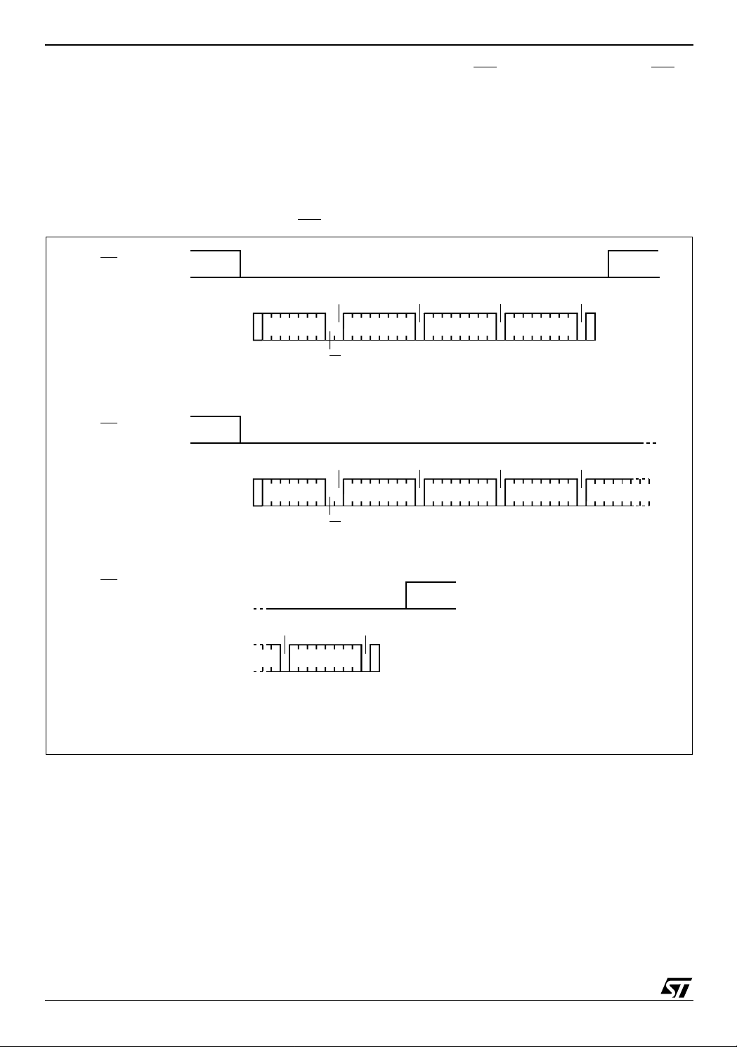
Figure 7. Wri te Mo de S e qu e nces with WC =1 (data wri te inhibi ted)
WC
ACK ACK ACK NO ACK
BYTE WRITE DEV SEL BYTE ADDR BYTE ADDR DATA IN
M24C64, M24C32
R/W
START
WC
ACK ACK ACK NO ACK
PAGE WRITE DEV SEL BYTE ADDR BYTE ADDR DATA IN 1
R/W
START
WC (cont'd)
NO ACK NO ACK
PAGE WRITE
(cont'd)
DATA IN N
STOP
slot), either at the end of a Byte Write or a Page
Write Operations
Following a Start condition the bus master sends
a Device Select Code with the RW
bit rese t to 0 .
The device acknowledges this, as shown in Figure
7, and waits for two address bytes. The device responds to each address byte with an acknowledge
bit, and then waits for the data byte.
Writing to the memory may be inhibited if Write
Control (WC
with Write Control (WC
) is driven High. Any Write instruction
) driven High (during a period of time from the Start condition until the end of
the two address bytes) will not modify the memory
contents, and the accompanying data bytes are
not
acknowledged, as shown in Figure 6.
Each data byte in the m emory has a 16-bit (two
byte wide) address. The Most Significant Byte (Table 3) is sent first, followed by the Least Significant
Byte (Table 4). Bits b15 to b0 form t he add ress of
the byte in memory.
When the bus mast er generates a Stop con dition
immediately after the Ack bi t (in t he “10
th
bit” time
Write, the internal memory Write cycle is triggered.
A Stop condition at any other time slot does not
trigger the internal Write cycle.
During the internal Write cycle, Serial Da ta (SDA)
is disabled internally, and the devi ce does not respond to any requests.
Byte Write
After the Device Select code and the address
bytes, the bus master sends one dat a byte. If the
addressed location is Write-protected, by Write
Control (WC
with NoAck, and the location is not modified. If, instead, the addressed location is not Write-protected, the device replies with Ack. The bus master
terminates the transfer by generating a S top condition, as shown in Figure 7.
Page Write
The Page Write mode allows u p to 32 by tes to be
written in a single Write cycle, provided that they
are all located in the same ’row’ in the memory:
that is, the most significant m emory address bits
STOP
DATA IN 2
AI01120C
) being driven High, the device replies
7/24
Page 8
M24C64, M24C32
(b12-b5 for M24C64, and b12-b5 for M24C32) are
the same. If more bytes are sent than will fit up to
the end of the row, a condition known as ‘roll-over’
occurs. This should be avoided, as data s tarts to
become overwritten in an implement ation dependent way.
The bus master sends fr om 1 to 32 bytes of data,
each of which is acknowledged by the device if
Figure 8. Wri te Mo de S e qu e nces with W
WC
BYTE WRITE DEV SEL BYTE ADDR BYTE ADDR DATA IN
START
WC
C=0 (data write enabled)
ACK
R/W
ACK ACK ACK ACK
Write Control (WC) is Low. If Write Control (WC) is
High, the contents of the addressed memory location are not modified, and each dat a byte is followed by a NoAck. After each byt e is transferred,
the internal byte address counte r (the 5 least s ignificant address bits only) is incremented. The
transfer is terminated by the bus master generating a Stop condition.
ACK ACK ACK
STOP
PAGE WRITE DEV SEL BYTE ADDR BYTE ADDR DATA IN 1
R/W
START
WC (cont'd)
ACKACK
PAGE WRITE
(cont'd)
DATA IN N
STOP
DATA IN 2
AI01106C
8/24
Page 9

Figure 9. Wri te Cy cle Pol l in g Fl owchart usin g A C K
WRITE Cycle
in Progress
START Condition
DEVICE SELECT
with RW = 0
ACK
NO
Returned
M24C64, M24C32
First byte of instruction
with RW = 0 already
decoded by the device
ReSTART
STOP
YES
Next
Operation is
Addressing the
Memory
DATA for the
WRITE Operation
Continue the
WRITE Operation
Minimizing System Delays by Polling On ACK
During the internal Write cycle, the device disconnects itself from the bus, and writes a copy of the
data from its internal latches to the memory cells.
The maximum Write time (t
) is shown in Tables
w
17 and 18, but the typical time is shorter. To make
use of this, a polling sequence can be used by the
bus master.
The sequence, as shown in Figure 8, is:
– Initial condition: a Write cycle is in progress.
YESNO
Send Address
and Receive ACK
START
Condition
YESNO
DEVICE SELECT
with RW = 1
Continue the
Random READ Operation
AI01847C
– Step 1: the bus master issues a Start condition
followed by a Device Select Code (the first byte
of the new instruction).
– Step 2: if the device is busy with the internal
Write cycle, no Ack will be returned and the bus
master goes back to Step 1. If the device has
terminated the internal Write cycle, it responds
with an Ack, indicating that the device is ready
to receive the second part of the instruction (the
first byte of this instruction having been sent
during Step 1).
9/24
Page 10

M24C64, M24C32
Figure 10. Read Mode Sequences
CURRENT ADDRESS READ
RANDOM ADDRESS READ
SEQUENTIAL
CURRENT
READ
SEQUENTIAL
RANDOM
READ
ACK
DEV SEL DATA OUT
R/W
START
ACK
DEV SEL * BYTE ADDR BYTE ADDR
R/W
START
ACK ACK ACK NO ACK
DEV SEL DATA OUT 1
R/W
START
ACK ACK ACK
DEV SEL * BYTE ADDR BYTE ADDR
NO ACK
STOP
ACK ACK ACK
DEV SEL * DATA OUT
R/W
START
DATA OUT N
STOP
ACK ACK
DEV SEL * DATA OUT 1
NO ACK
STOP
R/W
START
ACK NO ACK
DATA OUT N
STOP
Note: 1. The sev en m ost significant bits o f the Device Sel ect Code of a Random Read (in the 1st and 4th bytes) must be identical.
START
R/W
AI01105C
Current Address Read
Read Operations
Read operations are performed independently of
the state of the Write Control (WC
) signal.
Random Address Read
A dummy Write is performed to load the address
into the address counter (as shown in Figure 9) but
without
sending a Stop condition. Then, t he bus
master sends another Start condition, and repeats
the Device Select Code, with t he RW
bit set to 1.
The device acknowledges this, and outputs the
contents of the addressed byte. The bus master
must
not
acknowledge the byte, and terminates
the transfer with a Stop condition.
The device has an internal address counter which
is incremented each time a byte is read. For the
Current Address Read operation, following a Start
condition, the bus master only sends a Device Select Code with the RW
bit set to 1. The device acknowledges this, an d outpu ts the byt e address ed
by the internal address counter. The counter is
then incremented. The bus master t erm inates t he
transfer with a Stop condition, a s shown i n Figure
9,
without
acknowledging the byte.
Sequenti a l Rea d
This operation can be used after a Current Address Read or a Random Address Read. The bus
10/24
Page 11

M24C64, M24C32
master
does
acknowledge the data byte output,
and sends additional clock pulses so that the device continues to output the next byte in sequence.
To terminate the stream of bytes, the bus master
must
not
acknowledge the last byte, and
must
generate a Stop condition, as shown in Figure 9.
The output data comes from consecutive address-
es, with the internal address counter automatically
incremented after each byte output. After the last
memory address, the address counter ‘rolls-over’,
and the device continues to output data from
memory address 00h.
Acknowledge in Read Mode
For all Read commands, the device waits, after
each byte read, for an acknowledgment during the
th
bit time. If the bus master does not drive Serial
9
Data (SDA) Low during this time, the device terminates the data transfer and s witches to its St andby mode.
11/24
Page 12

M24C64, M24C32
MAXI MUM RATI N G
Stressing the device ab ove the rating listed in t he
Absolute Maximum Ratings" table may cause permanent damage to the device. These are stress
ratings only and operation of the device at these or
any other conditions ab ove those i ndicated in t he
Operating sections of this specificat ion is not im-
Table 6. Absolute Maximum Ratings
Symbol Parameter Min. Max. Unit
T
T
STG
LEAD
Storage Temperature –65 150 °C
Lead Temperature during
Soldering
PDIP: 10 seconds
SO: 20 seconds (max)
TSSOP: 20 seconds (max)
plied. Exposure to Absolute Maximum Rating conditions for extended periods may affect device
reliability. Refer also to the STMicroelectronics
SURE Program and ot her relevant quality documents.
1
1
260
235
235
°C
V
IO
V
CC
V
ESD
Note: 1. IPC/JEDEC J-STD-020 A
2. JEDEC Std J ESD22-A114A (C1=1 00 pF, R1=1500 Ω, R2=500 Ω)
Input or Output range –0.6 6.5 V
Supply Voltage –0.3 6.5 V
Electrostatic Discharge Voltage (Human Body model)
2
–4000 4000 V
12/24
Page 13

M24C64, M24C32
DC AND AC PARAMETERS
This section summarizes the operat ing and measurement conditions, and the DC and AC characteristics of the device. The parameters in t he DC
and AC Characteristic tables that follow are derived from tests performed under the Measure-
Table 7. Operating Conditions (M24Cxx)
Symbol Parameter Min. Max. Unit
ment Conditions summarized in the relevant
tables. Designers should chec k th at the o perat ing
conditions in their circuit matc h the meas urement
conditions when relying on the quoted parameters.
V
CC
T
A
Supply Voltage 4.5 5.5 V
Ambient Operating Temperature –40 8 5 °C
Table 8. Operating Conditions (M24Cxx-W)
Symbol Parameter Min. Ma x. Unit
V
CC
T
A
Supply Voltage 2.5 5.5 V
Ambient Operating Temperature –40 8 5 °C
Table 9. Operating Conditions (M24Cxx-R)
Symbol Parameter Min. Ma x. Unit
V
CC
T
A
Supply Voltage 1.8 5.5 V
Ambient Operating Temperature –40 8 5 °C
13/24
Page 14

M24C64, M24C32
Table 10. AC Measurement Conditions
Symbol Parameter Min. Max. Unit
C
L
Load Capacitance 100 pF
Input Rise and Fall Times 50 ns
Input Levels
Input and Output Timing Reference Levels
Figure 11. AC Measurement I/O Waveform
Input Levels
0.8V
CC
0.2V
CC
Table 11. Input Parameters
Symbol
C
IN
C
IN
Z
WCL
Z
WCH
t
NS
Note: 1. TA = 25 °C, f = 400 kHz
2. Sampled only, not 100% tested.
Input Capacitanc e (SDA) 8 pF
Input Capacitance (other pins) 6 pF
WC Input Impedance VIN < 0.5 V 5 20 k
WC Input Impedance
Pulse width ignored
(Input Filter on SCL and SDA)
Parameter
1,2
to 0.8V
0.2V
0.3V
Input and Output
Timing Reference Levels
0.7V
CC
0.3V
CC
AI00825B
CC
to 0.7V
CC
CC
CC
V
V
Test Condition Min. Max. Unit
Ω
V
> 0.7V
IN
CC
500 k
Ω
Single glitch 100 ns
14/24
Page 15

Table 12. DC Characteristics (M24Cxx)
Symbol Parameter
Input Leakage Current
I
LI
(SCL, SDA, E2, E1, E0)
Test Condition
(in addition to those in Table 7)
V
= VSS or V
IN
CC
device in Stand-by mode
M24C64, M24C32
Min. Max. Unit
± 2 µA
I
I
I
CC1
Output Leakage Current V
LO
Supply Current
CC
Stand-by Supply Current
V
Input Low Voltage
V
V
V
(E2, E1, E0, SCL, SDA)
IL
Input Low Voltage (WC
Input High Voltage
IH
(E2, E1, E0, SCL, SDA, WC
Output Low Voltage IOL = 3 mA, VCC = 5 V 0.4 V
OL
) –0.3
)
Table 13. DC Characteristics (M24Cxx-W)
Symbol Parameter
Input Leakage Current
I
LI
(SCL, SDA, E2, E1, E0)
I
I
I
CC1
V
Output Leakage Current V
LO
Supply Current
CC
Stand-by Supply Current
Input Low Voltage
(E2, E1, E0, SCL, SDA)
IL
Input Low Voltage (WC
) –0.3
V
CC
= VSS or V
OUT
=5V, fc=400kHz (rise/fall time < 30ns)
CC
V
= VSS or V
IN
SDA in Hi-Z ± 2 µA
CC,
, V
CC
= 5 V
CC
Test Condition
(in addition to those in Table 8)
V
= VSS or V
IN
CC
device in Stand-by mode
= VSS or V
OUT
SDA in Hi-Z ± 2 µA
CC,
=2.5V , fc=400kHz (rise/fall time < 30ns)
V
= VSS or V
IN
CC
, V
CC
= 2.5 V
–0.3 0.3V
0.7V
CC
Min.
–0.3 0.3V
2mA
10 µA
V
CC
0.5
VCC+1
V
V
Max. Unit
± 2 µA
1mA
2µA
V
CC
0.5
V
V
V
Input High Voltage
IH
(E2, E1, E0, SCL, SDA, WC
Output Low Voltage IOL = 2.1 mA, VCC = 2.5 V 0.4 V
OL
)
0.7V
CC
VCC+1 V
15/24
Page 16

M24C64, M24C32
Table 14. DC Characteristics (M24Cxx-R)
Symbol Parameter
Input Leakage Current
I
LI
(SCL, SDA, E2, E1, E0)
Test Condition
(in addition to those in Table 9)
V
= VSS or V
IN
CC
device in Stand-by mode
Min.
Max. Unit
± 2 µA
I
I
V
V
V
I
LO
CC
CC1
Output Leakage Current V
Supply Current
V
CC
Stand-by Supply Current
= VSS or V
OUT
=1.8V , fc=100kHz (rise/fall time < 30ns)
V
= VSS or V
IN
Input Low Voltage
(E2, E1, E0, SCL, SDA)
IL
Input Low Voltage (WC
Input High Voltage
IH
(E2, E1, E0, SCL, SDA, WC
Output Low Voltage IOL = 0.7 mA, VCC = 1.8 V
OL
) –0.3 0.5 V
)
SDA in Hi-Z ± 2 µA
CC,
0.8
, V
CC
= 1.8 V
CC
– 0.3
0.7V
CC
0.2
0.3 V
VCC+1 V
0.2
CC
mA
µA
V
V
16/24
Page 17

M24C64, M24C32
Table 15. AC Characteristics (M24Cxx, M24Cxx-W)
Test conditions specified in Table 10 and Table 7 or 8
Symbol Alt. Parameter Min. Max. Unit
f
C
t
CHCL
t
CLCH
t
DL1DL2
t
DXCX
t
CLDX
t
CLQX
3
t
CLQV
1
t
CHDX
t
DLCL
t
CHDH
t
DHDL
t
W
Note: 1. For a reS T A RT conditio n, or following a Write cy cle.
2. Sampled only, not 100% tested.
3. To avoid spurious START and STOP conditions, a minimum delay is placed between SCL=1 and the falling or rising edge of SDA.
4. The Write Tim e of 5 ms only appl i es to devices bearing the process let ter “B” in the package marking (on the to p side of the pac k-
age), otherwise (for devices bearing the process letter “N”) the Write Time is 10 ms. For further details, please contact your nearest
ST sales office, and ask fo r a copy of the Product Ch ange Notice PCEE0036.
f
SCL
t
HIGH
t
LOW
2
t
SU:DAT
t
HD:DAT
t
t
t
SU:STA
t
HD:STA
t
SU:STO
t
BUF
t
WR
Clock Frequency 400 kHz
Clock Pulse Width High 600 ns
Clock Pulse Width Low 1300 ns
t
SDA Fall Time 20 300 ns
F
Data In Set Up Time 100 ns
Data In Hold Time 0 ns
Data Out Hold Time 200 ns
DH
Clock Low to Next Data Valid (Access Time) 200 900 ns
AA
Start Condition Set Up Time 600 ns
Start Condition Hold Time 600 ns
Stop Condition Set Up Time 600 ns
Time between Stop Condition and Next Start Condition 1300 ns
Write Time
5 or
4
10
ms
Table 16. AC Characteristics (M24Cxx-R)
Test conditions specified in Table 10 and Table 9
Symbol Alt. Parameter Min. Max. Unit
f
C
t
CHCL
t
CLCH
t
DL1DL2
t
DXCX
t
CLDX
t
CLQX
3
t
CLQV
1
t
CHDX
t
DLCL
t
CHDH
t
DHDL
t
W
Note: 1. For a reS T A RT conditio n, or following a Write cy cle.
2. Sampled only, not 100% tested.
3. To avoid spurious START and STOP conditions, a minimum delay is placed between SCL=1 and the falling or rising edge of SDA.
f
SCL
t
HIGH
t
LOW
2
t
SU:DAT
t
HD:DAT
t
t
t
SU:STA
t
HD:STA
t
SU:STO
t
BUF
t
WR
Clock Frequency 400 kHz
Clock Pulse Width High 600 ns
Clock Pulse Width Low 1300 ns
t
SDA Fall Time 20 300 ns
F
Data In Set Up Time 100 ns
Data In Hold Time 0 ns
Data Out Hold Time 200 ns
DH
Clock Low to Next Data Valid (Access Time) 200 900 ns
AA
Start Condition Set Up Time 600 ns
Start Condition Hold Time 600 ns
Stop Condition Set Up Time 600 ns
Time between Stop Condition and Next Start Condition 1300 ns
Write Time 10 ms
17/24
Page 18

M24C64, M24C32
Figure 12. AC Waveforms
SCL
SDA In
SCL
SDA In
SCL
tCHCL
tDLCL
tCHDX
START
Condition
tCHDH
STOP
Condition
tCLQV tCLQX
SDA
Input
tCLCH
SDA
Change
tW
Write Cycle
tDXCXtCLDX
tCHDH tDHDL
tCHDX
START
Condition
STOP
Condition
START
Condition
SDA Out
Data Valid
AI00795C
18/24
Page 19

PACKAGE MECHANICAL
PDIP8 – 8 pin Plastic DIP, 0.25mm lead frame, Package Outline
M24C64, M24C32
b2
A2
A1AL
be
D
8
E1
1
Notes: 1. Drawing is not to scale.
E
c
eA
eB
PDIP-B
PDIP8 – 8 pin Plastic DIP, 0.25mm lead frame, Package Mechanical Data
Symb.
Typ. Min. Max. Typ. Min. Max.
A 5.33 0.210
A1 0.38 0.015
mm inches
A2 3.30 2.92 4.95 0.130 0.115 0.195
b 0.46 0.36 0.56 0.018 0.014 0.022
b2 1.52 1.14 1.78 0.060 0.045 0.070
c 0.25 0.20 0.36 0.010 0.008 0.014
D 9.27 9.02 10.16 0.365 0.355 0.400
E 7.87 7.62 8.26 0.310 0.300 0.325
E1 6.35 6.10 7.11 0.250 0.240 0.280
e 2.54 – – 0.100 – –
eA 7.62 – – 0.300 – –
eB 10.92 0.430
L 3.30 2.92 3.81 0.130 0.115 0.150
19/24
Page 20

M24C64, M24C32
SO8 narrow – 8 lead Plastic Small Outline, 150 mils body width, Package Ou tline
h x 45˚
Note: Drawing is not to scale.
B
SO-a
A
e
D
N
1
CP
E
H
C
LA1 α
SO8 narrow – 8 lead Plastic Small Outline, 150 mils body width, Package M echa nical Data
Symb.
Typ. Min. Max. Typ. Min. Max.
mm inches
20/24
A 1.35 1.75 0.053 0.069
A1 0.10 0.25 0.004 0.010
B 0.33 0.51 0.013 0.020
C 0.19 0.25 0.007 0.010
D 4.80 5.00 0.189 0.197
E 3.80 4.00 0.150 0.157
e 1.27 – – 0.050 – –
H 5.80 6.20 0.228 0.244
h 0.25 0.50 0.010 0.020
L 0.40 0.90 0.016 0.035
α
0° 8° 0° 8°
N8 8
CP 0.10 0.004
Page 21

TSSOP8 – 8 lead Thin Shrink Small Outline, Package Outline
D
M24C64, M24C32
8
1
CP
Notes: 1. Drawing is not to scale.
5
EE1
4
A2A
eb
A1
L1
TSSOP8 – 8 lead Thin Shrink Small Outline, Package Mec han ical Data
Symbol
Typ. Min. Max. Typ. Min. Max.
A 1.200 0.0472
A1 0.050 0.150 0.0020 0.0059
A2 1.000 0.800 1. 050 0.0394 0.0315 0.0413
b 0. 190 0.300 0.0075 0.0118
c 0.090 0.200 0.0035 0.0079
mm inches
c
α
L
TSSOP8AM
CP 0.100 0.0039
D 3.000 2.900 3.100 0.1181 0.1142 0.1 220
e 0 .650 – – 0.0256 – –
E 6.400 6.200 6. 600 0.2520 0.2441 0.2598
E1 4.400 4.300 4. 500 0.1732 0.1693 0.1772
L 0 .600 0.450 0.750 0.0236 0.0177 0.0295
L1 1 .000 0.0394
α
0° 8° 0° 8°
21/24
Page 22

M24C64, M24C32
PART NUMBERING
Table 17. Ordering Information Scheme
Example: M24C64 –WMN6T
Device Type
2
M24 = I
Device Function
64 = 64 Kbit (8192 x 8)
32 = 32 Kbit (4096 x 8)
Operating Voltage
blank = V
W = V
R = V
Package
BN = PDIP8
MN = SO8 (150 mil width)
DW = TSSOP8 (169 mil width)
C serial access EEPROM
= 4.5 to 5.5V
CC
= 2.5 to 5.5V
CC
= 1.8 to 5.5V
CC
Temperature Range
6 = –40 to 85 °C
Option
T = Tape & Reel Packing
Note: 1. Availa ble for M24C32 only.
For a list of available options (speed, package,
etc.) or for further information on any aspect of this
device, please contact your nearest ST Sales O ffice.
22/24
Page 23

M24C64, M24C32
REVISION HIST ORY
Table 18. Document Revision History
Date Rev. Description of Revision
22-Dec-1999 2.3 TSSOP8 package in place of TSSOP14 (pp 1, 2, OrderingInfo, PackageMechData).
28-Jun-2000 2.4 TSSOP8 package data corrected
31-Oct-2000 2.5
20-Apr-2001 2.6
16-Jan-2002 2.7
02-Aug-2002 2.8
04-Feb-2003 2.9 SO8W package removed. -S voltage range removed
27-May-2003 2.10 TSSOP8 (3x3mm² body size) package (MSOP8) removed
References to Temperature Range 3 removed from Ordering Information
Voltage range -S added, and range -R removed from text and tables throughout.
Lead Soldering Temperature in the Absolute Maximum Ratings table amended
Write Cycle Polling Flow Chart using ACK illustration updated
References to PSDIP changed to PDIP and Package Mechanical data updated
Test condition for I
-R voltage range added
Document reformated using new template.
TSSOP8 (3x3mm² body size) package (MSOP8) added.
5ms write time offered for 5V and 2.5V devices
made more precise, and value of ILI for E2-E0 and WC added
LI
23/24
Page 24

M24C64, M24C32
Information furnished is believed to be accurate an d rel i able. However, STMicroelectro ni cs assumes no responsibility for the consequen ces
of use of such information nor for any infringement of patents or other rights of third parties which may result from its use. No license is granted
by implic ation or otherwise under any patent or patent ri ghts of STM i croelectr onics. Sp ecifications mentioned in thi s publication are subject
to change without notice. This publication supersedes and replaces all information previously supplied. STMicroelectronics product s are not
authorized for use as cri tical comp onents in lif e support devi ces or systems without express written approv al of STMicroel ectronics.
The ST log o i s registered trademark of STMicroelectronics
All other nam es are the pro perty of their respect ive owners
© 2003 STMicroelectronics - All Rights Reserved
STMicroelectronics group of companies
Austra lia - Brazil - Canada - China - F i nl and - France - Germany - Hong Kong -
India - Israel - Italy - Japan - Malaysia - Malt a - M orocco - Singapore - Spain - Sweden - Switzerl and - Unite d Kingdom - United States.
www.st.com
24/24
 Loading...