

Page 1
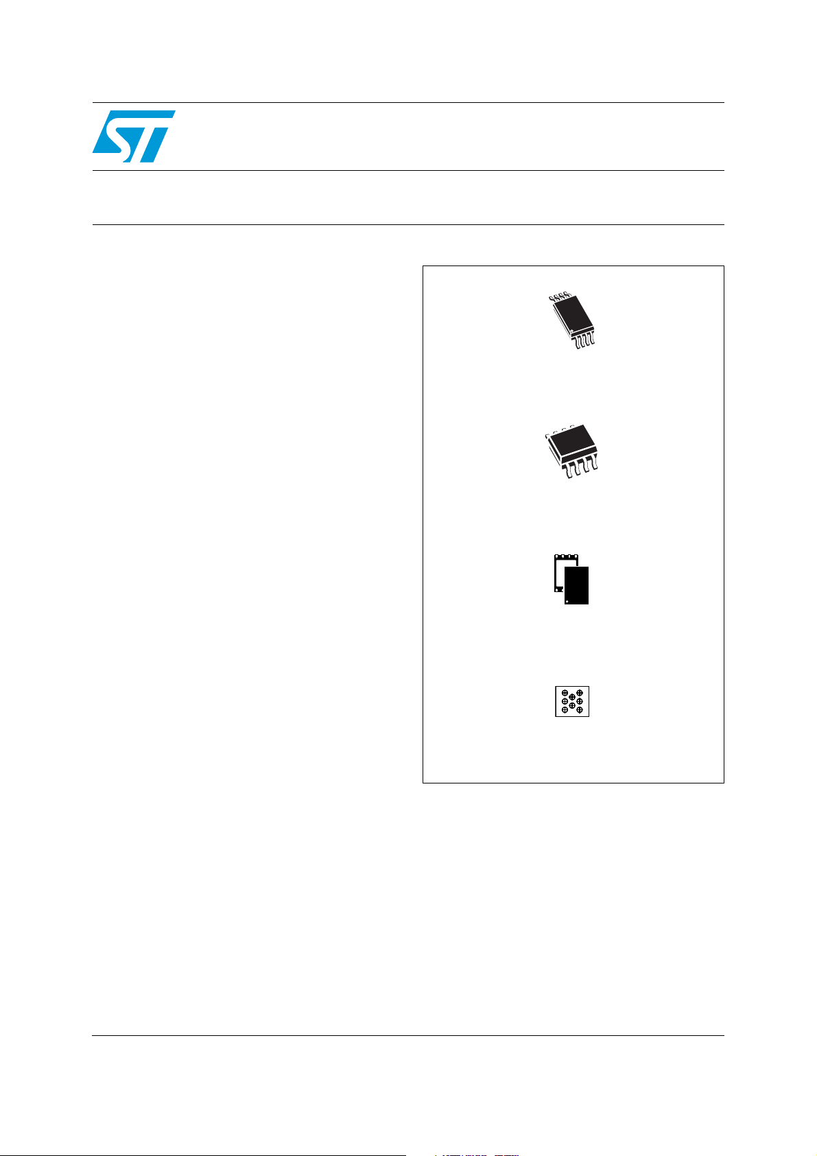
M24512-W M24512-R
SO8 (MN)
150 mil width
TSSOP8 (DW)
169 mil width
UFDFPN8
(MC)
WLCSP (CS)
M24512-DR M24512-DF
512-Kbit serial I²C bus EEPROM
Datasheet − production data
Features
■ Compatible with all I
–1 MHz
– 400 kHz
– 100 kHz
■ Single supply voltage and high speed:
– 1 MHz clock from 1.7 V to 5.5 V
■ Memory array:
– 512 Kbit (64 Kbytes) of EEPROM
– Page size: 128 bytes
– Additional Write lockable page
(M24512-D order codes)
■ Write
– Byte Write within 5 ms
– Page Write within 5 ms
■ Operating temperature range: from -40 °C up
to +85 °C
■ Random and sequential Read modes
■ Write protect of the whole memory array
■ Enhanced ESD/Latch-Up protection
■ More than 4 million Write cycles
■ More than 200-year data retention
■ Packages
– RoHS compliant and halogen-free
(ECOPACK
2
®
)
C bus modes:
June 2012 Doc ID 16459 Rev 25 1/44
This is information on a product in full production.
www.st.com
1
Page 2

Contents M24512-W M24512-R M24512-DR M24512-DF
Contents
1 Description . . . . . . . . . . . . . . . . . . . . . . . . . . . . . . . . . . . . . . . . . . . . . . . . . 6
2 Signal description . . . . . . . . . . . . . . . . . . . . . . . . . . . . . . . . . . . . . . . . . . . 8
2.1 Serial Clock (SCL) . . . . . . . . . . . . . . . . . . . . . . . . . . . . . . . . . . . . . . . . . . . 8
2.2 Serial Data (SDA) . . . . . . . . . . . . . . . . . . . . . . . . . . . . . . . . . . . . . . . . . . . . 8
2.3 Chip Enable (E2, E1, E0) . . . . . . . . . . . . . . . . . . . . . . . . . . . . . . . . . . . . . . 8
2.4 Write Control (WC
2.5 V
(ground) . . . . . . . . . . . . . . . . . . . . . . . . . . . . . . . . . . . . . . . . . . . . . . . 9
SS
2.6 Supply voltage (V
2.6.1 Operating supply voltage V
2.6.2 Power-up conditions . . . . . . . . . . . . . . . . . . . . . . . . . . . . . . . . . . . . . . . . 9
2.6.3 Device reset . . . . . . . . . . . . . . . . . . . . . . . . . . . . . . . . . . . . . . . . . . . . . . . 9
2.6.4 Power-down conditions . . . . . . . . . . . . . . . . . . . . . . . . . . . . . . . . . . . . . . 9
) . . . . . . . . . . . . . . . . . . . . . . . . . . . . . . . . . . . . . . . . . . . 8
) . . . . . . . . . . . . . . . . . . . . . . . . . . . . . . . . . . . . . . . . . 9
CC
CC . . . . . . . . . . . . . . . . . . . . . . . . . . . . . . . . . . . . . . . . . . 9
3 Memory organization . . . . . . . . . . . . . . . . . . . . . . . . . . . . . . . . . . . . . . . 10
4 Device operation . . . . . . . . . . . . . . . . . . . . . . . . . . . . . . . . . . . . . . . . . . . 11
4.1 Start condition . . . . . . . . . . . . . . . . . . . . . . . . . . . . . . . . . . . . . . . . . . . . . 12
4.2 Stop condition . . . . . . . . . . . . . . . . . . . . . . . . . . . . . . . . . . . . . . . . . . . . . 12
4.3 Data input . . . . . . . . . . . . . . . . . . . . . . . . . . . . . . . . . . . . . . . . . . . . . . . . . 12
4.4 Acknowledge bit (ACK) . . . . . . . . . . . . . . . . . . . . . . . . . . . . . . . . . . . . . . . 12
4.5 Device addressing . . . . . . . . . . . . . . . . . . . . . . . . . . . . . . . . . . . . . . . . . . 13
5 Instructions . . . . . . . . . . . . . . . . . . . . . . . . . . . . . . . . . . . . . . . . . . . . . . . 14
5.1 Write operations . . . . . . . . . . . . . . . . . . . . . . . . . . . . . . . . . . . . . . . . . . . . 14
5.1.1 Byte Write . . . . . . . . . . . . . . . . . . . . . . . . . . . . . . . . . . . . . . . . . . . . . . . 15
5.1.2 Page Write . . . . . . . . . . . . . . . . . . . . . . . . . . . . . . . . . . . . . . . . . . . . . . . 16
5.1.3 Write Identification Page (M24512-D only) . . . . . . . . . . . . . . . . . . . . . . 17
5.1.4 Lock Identification Page (M24512-D only) . . . . . . . . . . . . . . . . . . . . . . . 17
5.1.5 ECC (Error Correction Code) and Write cycling . . . . . . . . . . . . . . . . . . 18
5.1.6 Minimizing Write delays by polling on ACK . . . . . . . . . . . . . . . . . . . . . . 19
5.2 Read operations . . . . . . . . . . . . . . . . . . . . . . . . . . . . . . . . . . . . . . . . . . . . 20
5.2.1 Random Address Read . . . . . . . . . . . . . . . . . . . . . . . . . . . . . . . . . . . . . 20
2/44 Doc ID 16459 Rev 25
Page 3

M24512-W M24512-R M24512-DR M24512-DF Contents
5.2.2 Current Address Read . . . . . . . . . . . . . . . . . . . . . . . . . . . . . . . . . . . . . . 21
5.2.3 Sequential Read . . . . . . . . . . . . . . . . . . . . . . . . . . . . . . . . . . . . . . . . . . 21
5.3 Read Identification Page (M24512-D only) . . . . . . . . . . . . . . . . . . . . . . . 21
5.4 Read the lock status (M24512-D only) . . . . . . . . . . . . . . . . . . . . . . . . . . . 21
6 Initial delivery state . . . . . . . . . . . . . . . . . . . . . . . . . . . . . . . . . . . . . . . . . 22
7 Maximum rating . . . . . . . . . . . . . . . . . . . . . . . . . . . . . . . . . . . . . . . . . . . . 23
8 DC and AC parameters . . . . . . . . . . . . . . . . . . . . . . . . . . . . . . . . . . . . . . 24
9 Package mechanical data . . . . . . . . . . . . . . . . . . . . . . . . . . . . . . . . . . . . 33
10 Part numbering . . . . . . . . . . . . . . . . . . . . . . . . . . . . . . . . . . . . . . . . . . . . 38
11 Revision history . . . . . . . . . . . . . . . . . . . . . . . . . . . . . . . . . . . . . . . . . . . 39
Doc ID 16459 Rev 25 3/44
Page 4

List of tables M24512-W M24512-R M24512-DR M24512-DF
List of tables
Table 1. Signal names . . . . . . . . . . . . . . . . . . . . . . . . . . . . . . . . . . . . . . . . . . . . . . . . . . . . . . . . . . . . 6
Table 2. Device select code . . . . . . . . . . . . . . . . . . . . . . . . . . . . . . . . . . . . . . . . . . . . . . . . . . . . . . . 13
Table 3. Most significant address byte . . . . . . . . . . . . . . . . . . . . . . . . . . . . . . . . . . . . . . . . . . . . . . . 14
Table 4. Least significant address byte . . . . . . . . . . . . . . . . . . . . . . . . . . . . . . . . . . . . . . . . . . . . . . 14
Table 5. Absolute maximum ratings . . . . . . . . . . . . . . . . . . . . . . . . . . . . . . . . . . . . . . . . . . . . . . . . . 23
Table 6. Operating conditions (voltage range W) . . . . . . . . . . . . . . . . . . . . . . . . . . . . . . . . . . . . . . . 24
Table 7. Operating conditions (voltage range R) . . . . . . . . . . . . . . . . . . . . . . . . . . . . . . . . . . . . . . . 24
Table 8. Operating conditions (voltage range F) . . . . . . . . . . . . . . . . . . . . . . . . . . . . . . . . . . . . . . . 24
Table 9. AC measurement conditions. . . . . . . . . . . . . . . . . . . . . . . . . . . . . . . . . . . . . . . . . . . . . . . . 24
Table 10. Input parameters. . . . . . . . . . . . . . . . . . . . . . . . . . . . . . . . . . . . . . . . . . . . . . . . . . . . . . . . . 25
Table 11. Cycling performance by groups of four bytes . . . . . . . . . . . . . . . . . . . . . . . . . . . . . . . . . . . 25
Table 12. Memory cell data retention . . . . . . . . . . . . . . . . . . . . . . . . . . . . . . . . . . . . . . . . . . . . . . . . . 25
Table 13. DC characteristics (M24512-W, device grade 6) . . . . . . . . . . . . . . . . . . . . . . . . . . . . . . . . 26
Table 14. DC characteristics (M24512-R, M24512-DR, device grade 6) . . . . . . . . . . . . . . . . . . . . . . 27
Table 15. DC characteristics (M24512-DF, device grade 6). . . . . . . . . . . . . . . . . . . . . . . . . . . . . . . . 28
Table 16. 400 kHz AC characteristics. . . . . . . . . . . . . . . . . . . . . . . . . . . . . . . . . . . . . . . . . . . . . . . . . 29
Table 17. 1 MHz AC characteristics . . . . . . . . . . . . . . . . . . . . . . . . . . . . . . . . . . . . . . . . . . . . . . . . . . 30
Table 18. TSSOP8 – 8-lead thin shrink small outline, package mechanical data. . . . . . . . . . . . . . . . 33
Table 19. SO8N – 8 lead plastic small outline, 150 mils body width, package data. . . . . . . . . . . . . . 34
Table 20. UFDFPN8 (MLP8) 8-lead ultra thin fine pitch dual flat package no lead
2 x 3 mm, data . . . . . . . . . . . . . . . . . . . . . . . . . . . . . . . . . . . . . . . . . . . . . . . . . . . . . . . . . . 35
Table 21. M24512-DFCS6TP/K, WLCSP 8-bump wafer-level chip scale package mechanical data. 37
Table 22. Ordering information scheme . . . . . . . . . . . . . . . . . . . . . . . . . . . . . . . . . . . . . . . . . . . . . . . 38
4/44 Doc ID 16459 Rev 25
Page 5

M24512-W M24512-R M24512-DR M24512-DF List of figures
List of figures
Figure 1. Logic diagram . . . . . . . . . . . . . . . . . . . . . . . . . . . . . . . . . . . . . . . . . . . . . . . . . . . . . . . . . . . . 6
Figure 2. 8-pin package connections . . . . . . . . . . . . . . . . . . . . . . . . . . . . . . . . . . . . . . . . . . . . . . . . . . 7
Figure 3. WLCSP connections for die identified with process letters “KB”
(top view, marking side, with balls on the underside) . . . . . . . . . . . . . . . . . . . . . . . . . . . . . . 7
Figure 4. Device select code . . . . . . . . . . . . . . . . . . . . . . . . . . . . . . . . . . . . . . . . . . . . . . . . . . . . . . . . 8
Figure 5. Block diagram . . . . . . . . . . . . . . . . . . . . . . . . . . . . . . . . . . . . . . . . . . . . . . . . . . . . . . . . . . . 10
Figure 6. I
Figure 7. Write mode sequences with WC
Figure 8. Write mode sequences with WC
Figure 9. Write cycle polling flowchart using ACK . . . . . . . . . . . . . . . . . . . . . . . . . . . . . . . . . . . . . . . 19
Figure 10. Read mode sequences . . . . . . . . . . . . . . . . . . . . . . . . . . . . . . . . . . . . . . . . . . . . . . . . . . . . 20
Figure 11. AC measurement I/O waveform . . . . . . . . . . . . . . . . . . . . . . . . . . . . . . . . . . . . . . . . . . . . . 25
Figure 12. Maximum R
Figure 13. Maximum R
Figure 14. AC waveforms . . . . . . . . . . . . . . . . . . . . . . . . . . . . . . . . . . . . . . . . . . . . . . . . . . . . . . . . . . 32
Figure 15. TSSOP8 – 8-lead thin shrink small outline, package outline . . . . . . . . . . . . . . . . . . . . . . . 33
Figure 16. SO8N – 8 lead plastic small outline, 150 mils body width, package outline . . . . . . . . . . . . 34
Figure 17. UFDFPN8 (MLP8) - 8-lead ultra thin fine pitch dual flat no lead, package outline . . . . . . . 35
Figure 18. M24512-DFCS6TP/K , WLCSP 8-bump wafer-level chip scale package outline . . . . . . . . 36
2
C bus protocol . . . . . . . . . . . . . . . . . . . . . . . . . . . . . . . . . . . . . . . . . . . . . . . . . . . . . . . . . 11
= 0 (data write enabled) . . . . . . . . . . . . . . . . . . . . . . . . . 15
= 1 (data write inhibited) . . . . . . . . . . . . . . . . . . . . . . . . . 16
value versus bus parasitic capacitance (C
2
an I
C bus at maximum frequency fC = 400 kHz . . . . . . . . . . . . . . . . . . . . . . . . . . . . . . . . 31
2
an I
C bus at maximum frequency fC = 1MHz . . . . . . . . . . . . . . . . . . . . . . . . . . . . . . . . . . 31
bus
value versus bus parasitic capacitance C
bus
bus
bus
) for
) for
Doc ID 16459 Rev 25 5/44
Page 6
Description M24512-W M24512-R M24512-DR M24512-DF
!)F
%% 3$!
6
##
-XXX
7#
3#,
6
33
1 Description
The M24512 is a 512-Kbit I2C-compatible EEPROM (Electrically Erasable PROgrammable
Memory) organized as 64 K × 8 bits.
The M24512-W can operate with a supply voltage from 2.5 V to 5.5 V, the M24512-R and
M24512-DR can operate with a supply voltage from 1.8 V to 5.5 V and the M24512-DF can
operate with a supply voltage from 1.7 V to 5.5 V. All these devices operate with a clock
frequency of 1 MHz (or less) over an ambient temperature range of -40 °C / +85 °C.
The M24512-D offers an additional page, named the Identification Page (128 bytes). The
Identification Page can be used to store sensitive application parameters which can be
(later) permanently locked in Read-only mode.
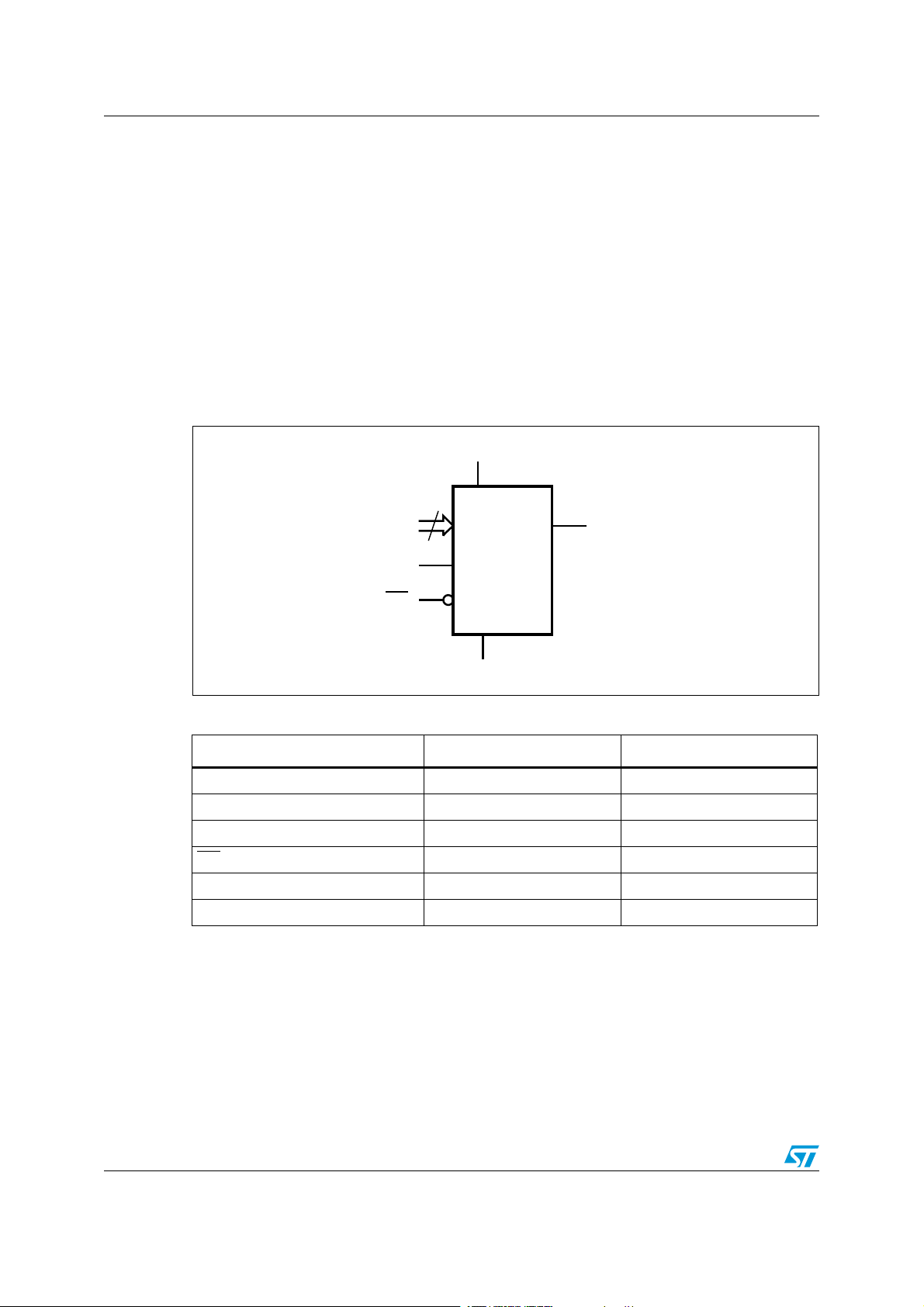
Figure 1. Logic diagram
Table 1. Signal names
Signal name Function Direction
E2, E1, E0 Chip Enable Input
SDA Serial Data I/O
SCL Serial Clock Input
WC
V
CC
V
SS
6/44 Doc ID 16459 Rev 25
Write Control Input
Supply voltage
Ground
Page 7
M24512-W M24512-R M24512-DR M24512-DF Description
3$!6
33
3#,
7#%
% 6
##
%
!)F
-36
6
##
3$!
6
33
%
3#,
%
7#
%
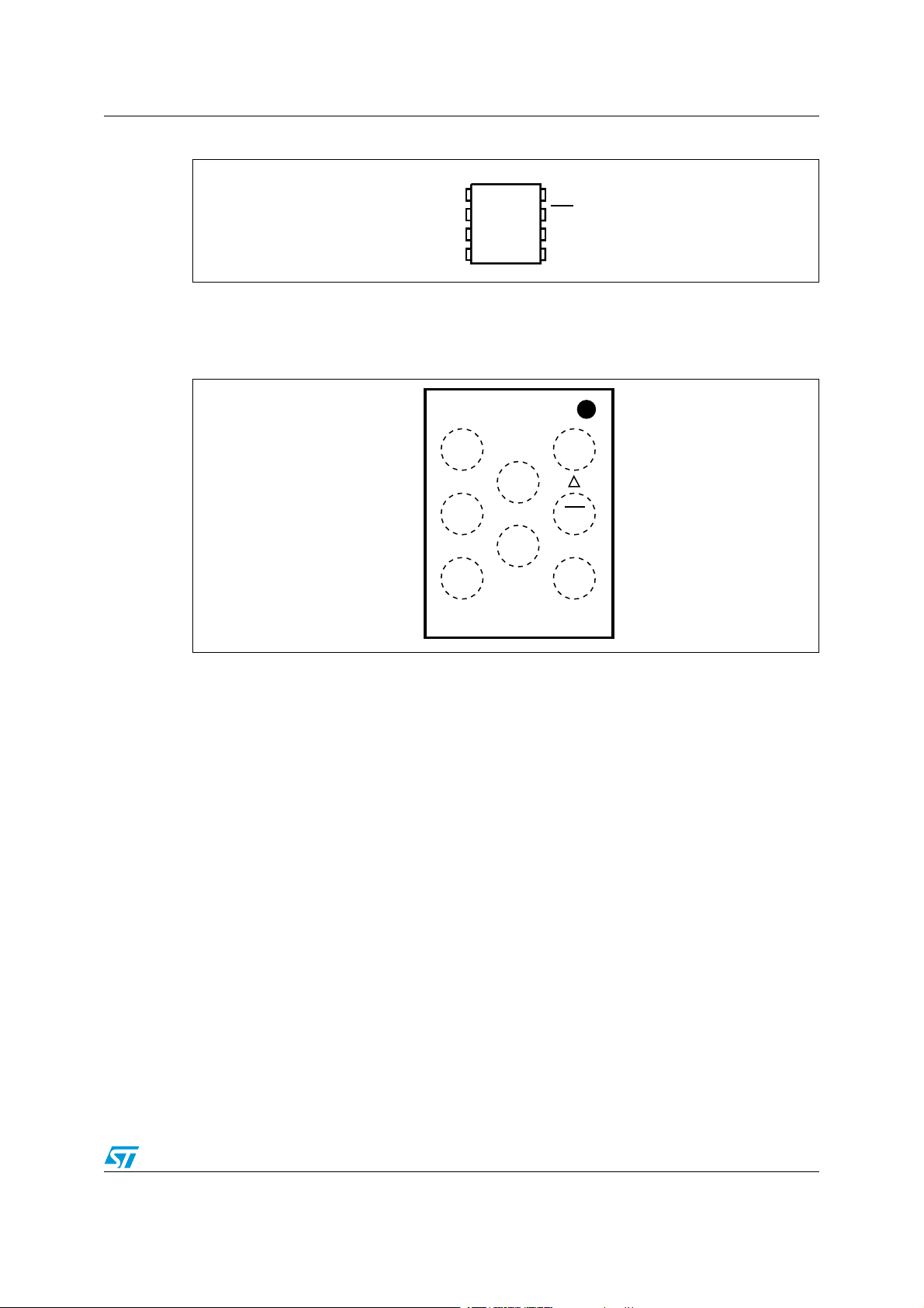
Figure 2. 8-pin package connections
1. DU: Don't Use (if connected, must be connected to VSS)
2. See Section 9: Package mechanical data for package dimensions, and how to identify pin 1.
Figure 3. WLCSP connections for die identified with process letters “KB”
(top view, marking side, with balls on the underside)
Caution: As EEPROM cells lose their charge (and so their binary value) when exposed to ultra violet
(UV) light, EEPROM dice delivered in wafer form or in WLCSP package by
STMicroelectronics must never be exposed to UV light.
Doc ID 16459 Rev 25 7/44
Page 8
Signal description M24512-W M24512-R M24512-DR M24512-DF
Ai12806
V
CC
M24xxx
V
SS
E
i
V
CC
M24xxx
V
SS
E
i
2 Signal description
2.1 Serial Clock (SCL)
The signal applied on the SCL input is used to strobe the data available on SDA(in) and to
output the data on SDA(out).
2.2 Serial Data (SDA)
SDA is an input/output used to transfer data in or data out of the device. SDA(out) is an open
drain output that may be wire-OR’ed with other open drain or open collector signals on the
bus. A pull-up resistor must be connected from Serial Data (SDA) to V
indicates how to calculate the value of the pull-up resistor).
2.3 Chip Enable (E2, E1, E0)
(E2,E1,E0) input signals are used to set the value that is to be looked for on the three least
significant bits (b3, b2, b1) of the 7-bit device select code (see Ta b le 2 ). These inputs must
be tied to V
are read as low (0).
or VSS, as shown in Figure 4. When not connected (left floating), these inputs
CC
(Figure 12
CC
Figure 4. Device select code
2.4 Write Control (WC)
This input signal is useful for protecting the entire contents of the memory from inadvertent
write operations. Write operations are disabled to the entire memory array when Write
Control (WC
driven low or left floating.
When Write Control (WC
acknowledged, Data bytes are not acknowledged.
) is driven high. Write operations are enabled when Write Control (WC) is either
) is driven high, device select and address bytes are
8/44 Doc ID 16459 Rev 25
Page 9

M24512-W M24512-R M24512-DR M24512-DF Signal description
2.5 VSS (ground)
VSS is the reference for the VCC supply voltage.
2.6 Supply voltage (VCC)
2.6.1 Operating supply voltage V
Prior to selecting the memory and issuing instructions to it, a valid and stable VCC voltage
within the specified [V
(min), VCC(max)] range must be applied (see Operating conditions
CC
in Section 8: DC and AC parameters). In order to secure a stable DC supply voltage, it is
recommended to decouple the V
10 nF to 100 nF) close to the V
CC
CC/VSS
This voltage must remain stable and valid until the end of the transmission of the instruction
and, for a write instruction, until the completion of the internal write cycle (t
2.6.2 Power-up conditions
The VCC voltage has to rise continuously from 0 V up to the minimum VCC operating voltage
(see Operating conditions in Section 8: DC and AC parameters) and the rise time must not
vary faster than 1 V/µs.
2.6.3 Device reset
In order to prevent inadvertent write operations during power-up, a power-on-reset (POR)
circuit is included.
At power-up, the device does not respond to any instruction until V
internal reset threshold voltage. This threshold is lower than the minimum V
voltage (see Operating conditions in Section 8: DC and AC parameters). When V
over the POR threshold, the device is reset and enters the Standby Power mode; however,
the device must not be accessed until V
specified [V
parameters).
(min), VCC(max)] range (see Operating conditions in Section 8: DC and AC
CC
CC
line with a suitable capacitor (usually of the order of
package pins.
).
W
has reached the
CC
reaches a valid and stable DC voltage within the
CC
operating
CC
CC
passes
In a similar way, during power-down (continuous decrease in V
accessed when V
drops below VCC(min). When VCC drops below the power-on-reset
CC
threshold voltage, the device stops responding to any instruction sent to it.
2.6.4 Power-down conditions
During power-down (continuous decrease in VCC), the device must be in the Standby Power
mode (mode reached after decoding a Stop condition, assuming that there is no internal
write cycle in progress).
), the device must not be
CC
Doc ID 16459 Rev 25 9/44
Page 10
Memory organization M24512-W M24512-R M24512-DR M24512-DF
-36
7#
#ONTROLLOGIC
(IGHVOLTAGE
GENERATOR
)/SHIFTREGISTER
!DDRESSREGISTER
ANDCOUNTER
$ATA
REGISTER
PAGE
8DECODER
9DECODER
)DENTIFICATIONPAGE
%
%
3#,
3$!
%
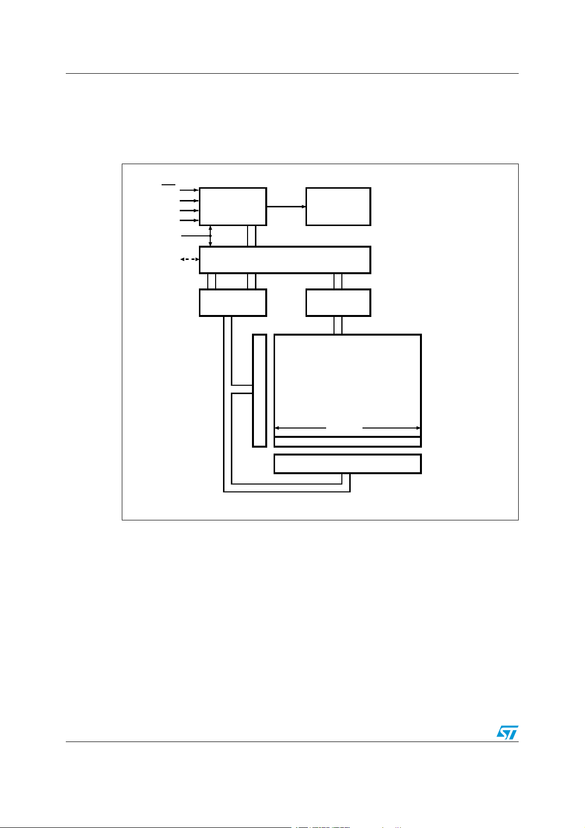
3 Memory organization
The memory is organized as shown below.
Figure 5. Block diagram
10/44 Doc ID 16459 Rev 25
Page 11
M24512-W M24512-R M24512-DR M24512-DF Device operation
SCL
SDA
SCL
SDA
SDA
START
Condition
SDA
Input
SDA
Change
AI00792B
STOP
Condition
1 23 7 89
MSB
ACK
START
Condition
SCL
1 23 7 89
MSB ACK
STOP
Condition
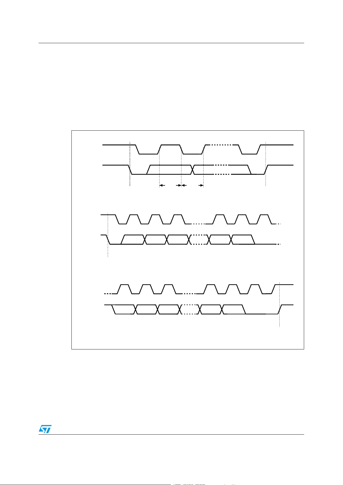
4 Device operation
The device supports the I2C protocol. This is summarized in Figure 6. Any device that sends
data on to the bus is defined to be a transmitter, and any device that reads the data to be a
receiver. The device that controls the data transfer is known as the bus master, and the
other as the slave device. A data transfer can only be initiated by the bus master, which will
also provide the serial clock for synchronization. The device is always a slave in all
communications.
Figure 6. I
2
C bus protocol
Doc ID 16459 Rev 25 11/44
Page 12

Device operation M24512-W M24512-R M24512-DR M24512-DF
4.1 Start condition
Start is identified by a falling edge of Serial Data (SDA) while Serial Clock (SCL) is stable in
the high state. A Start condition must precede any data transfer instruction. The device
continuously monitors (except during a Write cycle) Serial Data (SDA) and Serial Clock
(SCL) for a Start condition.
4.2 Stop condition
Stop is identified by a rising edge of Serial Data (SDA) while Serial Clock (SCL) is stable
and driven high. A Stop condition terminates communication between the device and the
bus master. A Read instruction that is followed by NoAck can be followed by a Stop
condition to force the device into the Standby mode.
A Stop condition at the end of a Write instruction triggers the internal Write cycle.
4.3 Data input
During data input, the device samples Serial Data (SDA) on the rising edge of Serial Clock
(SCL). For correct device operation, Serial Data (SDA) must be stable during the rising edge
of Serial Clock (SCL), and the Serial Data (SDA) signal must change only when Serial Clock
(SCL) is driven low.
4.4 Acknowledge bit (ACK)
The acknowledge bit is used to indicate a successful byte transfer. The bus transmitter,
whether it be bus master or slave device, releases Serial Data (SDA) after sending eight bits
of data. During the 9
acknowledge the receipt of the eight data bits.
th
clock pulse period, the receiver pulls Serial Data (SDA) low to
12/44 Doc ID 16459 Rev 25
Page 13
M24512-W M24512-R M24512-DR M24512-DF Device operation
4.5 Device addressing
To start communication between the bus master and the slave device, the bus master must
initiate a Start condition. Following this, the bus master sends the device select code, shown
in Ta ble 2 (on Serial Data (SDA), most significant bit first).
Table 2. Device select code
Device type identifier
b7 b6 b5 b4 b3 b2 b1 b0
Device select code
when addressing the
memory array
Device select code
when accessing the
Identification page
1. The most significant bit, b7, is sent first.
2. E0, E1 and E2 are compared against the respective external pins on the memory device.
1010E2E1E0RW
1011E2E1E0RW
(1)
Chip Enable address
When the device select code is received, the device only responds if the Chip Enable
Address is the same as the value on the Chip Enable (E2, E1, E0) inputs.
th
The 8
bit is the Read/Write bit (RW). This bit is set to 1 for Read and 0 for Write operations.
(2)
RW
If a match occurs on the device select code, the corresponding device gives an
acknowledgment on Serial Data (SDA) during the 9
th
bit time. If the device does not match
the device select code, it deselects itself from the bus, and goes into Standby mode.
Doc ID 16459 Rev 25 13/44
Page 14
Instructions M24512-W M24512-R M24512-DR M24512-DF
5 Instructions
5.1 Write operations
Following a Start condition the bus master sends a device select code with the R/W bit (RW)
reset to 0. The device acknowledges this, as shown in Figure 7, and waits for two address
bytes. The device responds to each address byte with an acknowledge bit, and then waits
for the data byte.
Table 3. Most significant address byte
A15 A14 A13 A12 A11 A10 A9 A8
Table 4. Least significant address byte
A7 A6 A5 A4 A3 A2 A1 A0
When the bus master generates a Stop condition immediately after a data byte Ack bit (in
the “10
cycle t
th
bit” time slot), either at the end of a Byte Write or a Page Write, the internal Write
is triggered. A Stop condition at any other time slot does not trigger the internal
W
Write cycle.
After the Stop condition and the successful completion of an internal Write cycle (t
), the
W
device internal address counter is automatically incremented to point to the next byte after
the last modified byte.
During the internal Write cycle, Serial Data (SDA) is disabled internally, and the device does
not respond to any requests.
If the Write Control input (WC) is driven High, the Write instruction is not executed and the
accompanying data bytes are not acknowledged, as shown in Figure 8.
14/44 Doc ID 16459 Rev 25
Page 15

M24512-W M24512-R M24512-DR M24512-DF Instructions
Stop
Start
Byte Write Dev sel Byte addr
Byte addr Data in
WC
Start
Page Write Dev sel Byte addr Byte addr Data in 1
WC
Data in 2
AI01106d
Page Write (cont'd)
WC (cont'd)
Stop
Data in N
ACK
R/W
ACK ACK ACK
ACK ACK ACK ACK
R/W
ACKACK
5.1.1 Byte Write
After the device select code and the address bytes, the bus master sends one data byte. If
the addressed location is Write-protected, by Write Control (WC
device replies with NoAck, and the location is not modified. If, instead, the addressed
location is not Write-protected, the device replies with Ack. The bus master terminates the
transfer by generating a Stop condition, as shown in Figure 7.
) being driven high, the
Figure 7. Write mode sequences with WC
= 0 (data write enabled)
Doc ID 16459 Rev 25 15/44
Page 16

Instructions M24512-W M24512-R M24512-DR M24512-DF
Stop
Start
Byte Write Dev sel Byte addr Byte addr Data in
WC
Start
Page Write Dev sel Byte addr Byte addr Data in 1
WC
Data in 2
AI01120d
Page Write (cont'd)
WC (cont'd)
Stop
Data in N
ACK ACK ACK NO ACK
R/W
ACK ACK ACK NO ACK
R/W
NO ACK NO ACK
5.1.2 Page Write
The Page Write mode allows up to 128 bytes to be written in a single Write cycle, provided
that they are all located in the same page in the memory: that is, the most significant
memory address bits, A15/A7, are the same. If more bytes are sent than will fit up to the end
of the page, a “roll-over” occurs, i.e. the bytes exceeding the page end are written on the
same page, from location 0.
The bus master sends from 1 to 128 bytes of data, each of which is acknowledged by the
device if Write Control (WC
addressed memory location are not modified, and each data byte is followed by a NoAck, as
shown in Figure 8. After each transferred byte, the internal page address counter is
incremented.
The transfer is terminated by the bus master generating a Stop condition.
) is low. If Write Control (WC) is high, the contents of the
Figure 8. Write mode sequences with WC
= 1 (data write inhibited)
16/44 Doc ID 16459 Rev 25
Page 17

M24512-W M24512-R M24512-DR M24512-DF Instructions
5.1.3 Write Identification Page (M24512-D only)
The Identification Page (128 bytes) is an additional page which can be written and (later)
permanently locked in Read-only mode. It is written by issuing the Write Identification Page
instruction. This instruction uses the same protocol and format as Page Write (into memory
array), except for the following differences:
● Device type identifier = 1011b
● MSB address bits A15/A7 are don't care except for address bit A10 which must be ‘0’.
LSB address bits A6/A0 define the byte address inside the Identification page.
If the Identification page is locked, the data bytes transferred during the Write Identification
Page instruction are not acknowledged (NoAck).
5.1.4 Lock Identification Page (M24512-D only)
The Lock Identification Page instruction (Lock ID) permanently locks the Identification page
in Read-only mode. The Lock ID instruction is similar to Byte Write (into memory array) with
the following specific conditions:
● Device type identifier = 1011b
● Address bit A10 must be ‘1’; all other address bits are don't care
● The data byte must be equal to the binary value xxxx xx1x, where x is don't care
If the Identification Page is locked, the data bytes transferred during the Write Identification
Page instruction are not acknowledged (NoAck).
Doc ID 16459 Rev 25 17/44
Page 18

Instructions M24512-W M24512-R M24512-DR M24512-DF
5.1.5 ECC (Error Correction Code) and Write cycling
The Error Correction Code (ECC) is an internal logic function which is transparent for the
2
I
C communication protocol.
The ECC logic is implemented on each group of four EEPROM bytes
single bit out of the four bytes happens to be erroneous during a Read operation, the ECC
detects this bit and replaces it with the correct value. The read reliability is therefore much
improved.
Even if the ECC function is performed on groups of four bytes, a single byte can be
written/cycled independently. In this case, the ECC function also writes/cycles the three
other bytes located in the same group
(a)
. As a consequence, the maximum cycling budget is
defined at group level and the cycling can be distributed over the 4 bytes of the group: the
sum of the cycles seen by byte0, byte1, byte2 and byte3 of the same group must remain
below the maximum value defined in Table 11: Cycling performance by groups of four bytes.
(a)
. Inside a group, if a
a. A group of four bytes is located at addresses [4*N, 4*N+1, 4*N+2, 4*N+3], where N is an
integer.
18/44 Doc ID 16459 Rev 25
Page 19

M24512-W M24512-R M24512-DR M24512-DF Instructions
Write cycle
in progress
AI
d
AI01847e
Next
Operation is
addressing the
memory
Start condition
Device select
with RW = 0
ACK
returned
YES
NO
YESNO
ReStart
Stop
Data for the
Write cperation
Device select
with RW = 1
Send Address
and Receive ACK
First byte of instruction
with RW = 0 already
decoded by the device
YESNO
StartCondition
Continue the
Write operation
Continue the
Random Read operation
5.1.6 Minimizing Write delays by polling on ACK
The maximum Write time (tw) is shown in AC characteristics tables in Section 8: DC and AC
parameters, but the typical time is shorter. To make use of this, a polling sequence can be
used by the bus master.
The sequence, as shown in Figure 9, is:
● Initial condition: a Write cycle is in progress.
● Step 1: the bus master issues a Start condition followed by a device select code (the
first byte of the new instruction).
● Step 2: if the device is busy with the internal Write cycle, no Ack will be returned and
the bus master goes back to Step 1. If the device has terminated the internal Write
cycle, it responds with an Ack, indicating that the device is ready to receive the second
part of the instruction (the first byte of this instruction having been sent during Step 1).
Figure 9. Write cycle polling flowchart using ACK
1. The seven most significant bits of the Device Select code of a Random Read (bottom right box in the
figure) must be identical to the seven most significant bits of the Device Select code of the Write (polling
instruction in the figure).
Doc ID 16459 Rev 25 19/44
01847
Page 20

Instructions M24512-W M24512-R M24512-DR M24512-DF
Start
Dev sel * Byte addr Byte addr
Start
Dev sel Data out 1
AI01105d
Data out N
Stop
Start
Current
Address
Read
Dev sel Data out
Random
Address
Read
Stop
Start
Dev sel * Data out
Sequential
Current
Read
Stop
Data out N
Start
Dev sel * Byte addr Byte addr
Sequention
Random
Read
Start
Dev sel * Data out1
Stop
ACK
R/W
NO ACK
ACK
R/W
ACK ACK ACK
R/W
ACK ACK ACK NO ACK
R/W
NO ACK
ACK ACK ACK
R/W
ACK ACK
R/W
ACK NO ACK
5.2 Read operations
Read operations are performed independently of the state of the Write Control (WC) signal.
After the successful completion of a Read operation, the device’s internal address counter is
incremented by one, to point to the next byte address.
For the Read instructions, after each byte read (data out), the device waits for an
acknowledgment (data in) during the 9th bit time. If the bus master does not acknowledge
during this 9th time, the device terminates the data transfer and switches to its Standby
mode.
Figure 10. Read mode sequences
5.2.1 Random Address Read
A dummy Write is first performed to load the address into this address counter (as shown in
Figure 10) but without sending a Stop condition. Then, the bus master sends another Start
condition, and repeats the device select code, with the RW
acknowledges this, and outputs the contents of the addressed byte. The bus master must
not acknowledge the byte, and terminates the transfer with a Stop condition.
20/44 Doc ID 16459 Rev 25
bit set to 1. The device
Page 21

M24512-W M24512-R M24512-DR M24512-DF Instructions
5.2.2 Current Address Read
For the Current Address Read operation, following a Start condition, the bus master only
sends a device select code with the R/W
outputs the byte addressed by the internal address counter. The counter is then
incremented. The bus master terminates the transfer with a Stop condition, as shown in
Figure 10, without acknowledging the byte.
bit set to 1. The device acknowledges this, and
5.2.3 Sequential Read
This operation can be used after a Current Address Read or a Random Address Read. The
bus master does acknowledge the data byte output, and sends additional clock pulses so
that the device continues to output the next byte in sequence. To terminate the stream of
bytes, the bus master must not acknowledge the last byte, and must generate a Stop
condition, as shown in Figure 10.
The output data comes from consecutive addresses, with the internal address counter
automatically incremented after each byte output. After the last memory address, the
address counter “rolls-over”, and the device continues to output data from memory address
00h.
5.3 Read Identification Page (M24512-D only)
The Identification Page (128 bytes) is an additional page which can be written and (later)
permanently locked in Read-only mode.
The Identification Page can be read by issuing an Read Identification Page instruction. This
instruction uses the same protocol and format as the Random Address Read (from memory
array) with device type identifier defined as 1011b. The MSB address bits A15/A7 are don't
care, the LSB address bits A6/A0 define the byte address inside the Identification Page. The
number of bytes to read in the ID page must not exceed the page boundary (e.g.: when
reading the Identification Page from location 100d, the number of bytes should be less than
or equal to 28, as the ID page boundary is 128 bytes).
5.4 Read the lock status (M24512-D only)
The locked/unlocked status of the Identification page can be checked by transmitting a
specific truncated command [Identification Page Write instruction + one data byte] to the
device. The device returns an acknowledge bit if the Identification page is unlocked,
otherwise a NoAck bit if the Identification page is locked.
Right after this, it is recommended to transmit to the device a Start condition followed by a
Stop condition, so that:
● Start: the truncated command is not executed because the Start condition resets the
device internal logic,
● Stop: the device is then set back into Standby mode by the Stop condition.
Doc ID 16459 Rev 25 21/44
Page 22

Initial delivery state M24512-W M24512-R M24512-DR M24512-DF
6 Initial delivery state
The device is delivered with all bits set to 1 (both in the memory array and in the
Identification page - that is, each byte contains FFh).
22/44 Doc ID 16459 Rev 25
Page 23

M24512-W M24512-R M24512-DR M24512-DF Maximum rating
7 Maximum rating
Stressing the device outside the ratings listed in Ta bl e 5 may cause permanent damage to
the device. These are stress ratings only, and operation of the device at these, or any other
conditions outside those indicated in the operating sections of this specification, is not
implied. Exposure to absolute maximum rating conditions for extended periods may affect
device reliability.
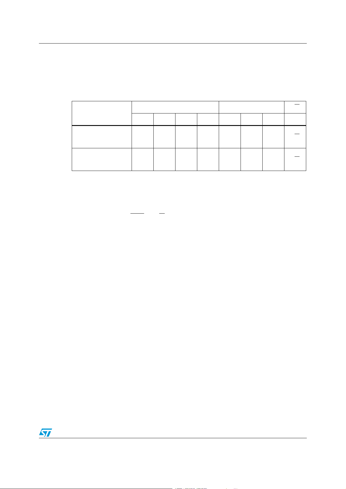
Table 5. Absolute maximum ratings
Symbol Parameter Min. Max. Unit
Ambient operating temperature –55 130 °C
T
STG
T
LEAD
V
IO
I
OL
V
CC
V
ESD
1. Compliant with JEDEC Std J-STD-020D (for small body, Sn-Pb or Pb assembly), the ST ECOPACK®
7191395 specification, and the European directive on Restrictions on Hazardous Substances (RoHS)
2002/95/EU.
2. Positive and negative pulses applied on different combinations of pin connections, according to AEC-
Q100-002 (compliant with JEDEC Std JESD22-A114, C1=100 pF, R1=1500 Ω).
3. 4000 V for new devices identified with process letters KB and 3000 V for previous devices identified with
process letters KA and AB.
Storage temperature –65 150 °C
Lead temperature during soldering see note
(1)
°C
Input or output range –0.50 6.5 V
DC output current (SDA = 0) - 5 mA
Supply voltage –0.50 6.5 V
Electrostatic pulse (Human Body model)
(2)
- 4000
(3)
V
Doc ID 16459 Rev 25 23/44
Page 24

DC and AC parameters M24512-W M24512-R M24512-DR M24512-DF
8 DC and AC parameters
This section summarizes the operating and measurement conditions, and the DC and AC
characteristics of the device.
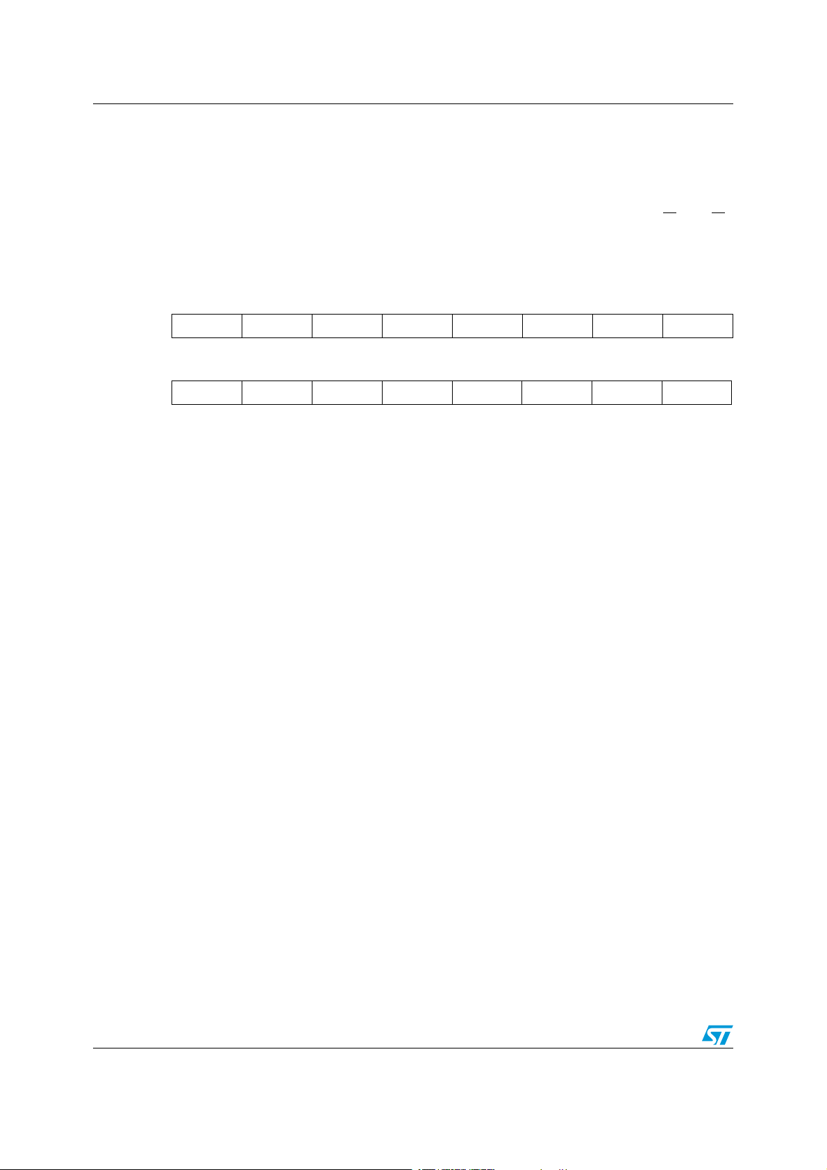
Table 6. Operating conditions (voltage range W)
Symbol Parameter Min. Max. Unit
V
CC
T
f
C
1. For devices identified by process letter K.
Table 7. Operating conditions (voltage range R)
Supply voltage 2.5 5.5 V
Ambient operating temperature –40 85 °C
A
Operating clock frequency - 1
(1)
Symbol Parameter Min. Max. Unit
V
CC
T
f
C
1. For devices identified by process letter K.
Table 8. Operating conditions (voltage range F)
Supply voltage 1.8 5.5 V
Ambient operating temperature –40 85 °C
A
Operating clock frequency - 1
(1)
Symbol Parameter Min. Max. Unit
V
CC
T
f
C
1. For devices identified by process letter K.
Supply voltage 1.7 5.5 V
Ambient operating temperature –40 85 °C
A
Operating clock frequency - 1
(1)
MHz
MHz
MHz
Table 9. AC measurement conditions
Symbol Parameter Min. Max. Unit
C
bus
Load capacitance 100 pF
SCL input rise/fall time, SDA input fall time 50 ns
Input levels 0.2 V
Input and output timing reference levels 0.3 V
24/44 Doc ID 16459 Rev 25
to 0.8 V
CC
to 0.7 V
CC
CC
CC
V
V
Page 25

M24512-W M24512-R M24512-DR M24512-DF DC and AC parameters
-36
6
##
6
##
6
##
6
##
)NPUTANDOUTPUT
4IMINGREFERENCELEVELS
)NPUTVOLTAGELEVELS
Figure 11. AC measurement I/O waveform
Table 10. Input parameters
Symbol Parameter
(1)
Test condition Min. Max. Unit
C
C
Z
Z
1. Characterized only, not tested in production.
2. E2, E1, E0 input impedance when the memory is selected (after a Start condition).
Table 11. Cycling performance by groups of four bytes
Symbol Parameter Test condition
Ncycle
1. Cycling performance for products identified by process letter KB.
2. The Write cycle endurance is defined for groups of four data bytes located at addresses [4*N, 4*N+1,
4*N+2, 4*N+3] where N is an integer. The Write cycle endurance is defined by characterization and
qualification.
3. A Write cycle is executed when either a Page Write, a Byte Write, a Write Identification Page or a Lock
Identification Page instruction is decoded. When using the Byte Write, the Page Write or the Write
Identification Page, refer also to Section 5.1.5: ECC (Error Correction Code) and Write cycling.
Table 12. Memory cell data retention
Input capacitance (SDA) 8 pF
IN
Input capacitance (other pins) 6 pF
IN
L
Input impedance (E2, E1, E0, WC)
H
Write cycle
endurance
TA ≤ 25 °C, VCC(min) < VCC < VCC(max) 4,000,000
(2)
TA = 85 °C, VCC(min) < VCC < VCC(max) 1,200,000
(2)
VIN < 0.3 V
VIN > 0.7 V
(1)
CC
CC
30 kΩ
500 kΩ
Max. Unit
Write cycle
Parameter Test condition Min. Unit
Data retention
1. For products identified by process letter KB. The data retention behavior is checked in production. The
200-year limit is defined from characterization and qualification results.
(1)
TA = 55 °C 200 Year
(3)
Doc ID 16459 Rev 25 25/44
Page 26

DC and AC parameters M24512-W M24512-R M24512-DR M24512-DF
Table 13. DC characteristics (M24512-W, device grade 6)
Symbol Parameter
Input leakage current
I
(SCL, SDA, E2, E1,
LI
E0)
Output leakage
I
LO
current
I
Supply current (Read)
CC
I
I
Supply current (Write) During tW, 2.5 V < VCC < 5.5 V 5
CC0
Standby supply
CC1
current
Input low voltage
V
IL
(SCL, SDA, WC)
Input high voltage
(SCL, SDA)
V
IH
Input high voltage
(WC, E2, E1, E0)
V
1. For devices identified by process letter AB: ICC(max) = 1 mA.
2. Characterized value, not tested in production.
3. The device is not selected after power-up, after a Read instruction (after the Stop condition), or after the
Output low voltage
OL
completion of the internal write cycle t
Test conditions (see Tabl e 6 and
Table 9 )
V
= VSS or V
IN
CC
Min. Max. Unit
device in Standby mode
SDA in Hi-Z, external voltage applied
on SDA: VSS or V
= 2.5 V, fc = 400 kHz
V
CC
CC
(rise/fall time < 50 ns)
V
= 5.5 V, fc = 400 kHz
CC
(rise/fall time < 50 ns)
2.5 V < V
< 5.5 V, fc = 1 MHz
CC
(rise/fall time < 50 ns)
(3)
, V
Device not selected
VCC, V
CC
= 2.5 V
Device not selected, V
= 5.5 V
V
CC
= VSS or
IN
= VSS or VCC,
IN
–0.45 0.3 V
0.7 V
CC
0.7 V
CCVCC
IOL = 2.1 mA, VCC = 2.5 V or
= 3 mA, VCC = 5.5 V
I
OL
(tW is triggered by the correct decoding of a Write instruction).
W
± 2 µA
± 2 µA
(1)
2
2mA
2.5 mA
(2)
2µA
3µA
CC
6.5 V
+0.6 V
0.4 V
mA
mA
V
26/44 Doc ID 16459 Rev 25
Page 27

M24512-W M24512-R M24512-DR M24512-DF DC and AC parameters
Table 14. DC characteristics (M24512-R, M24512-DR, device grade 6)
(1)
Symbol Parameter
Input leakage current
I
LI
(E1, E2, SCL, SDA)
I
Output leakage current
LO
Supply current (Read)
I
CC
I
I
Supply current (Write) During t
CC0
Standby supply current
CC1
Input low voltage
V
IL
(SCL, SDA, WC)
Input high voltage
(SCL, SDA)
V
IH
Input high voltage
(WC, E2, E1, E0)
V
1. If the application uses the voltage range R device with 2.5 V < Vcc < 5.5 V and -40 °C < TA < +85 °C,
2. For devices identified by process letters K: ICC(max) = 1.5 mA.
3. Only for devices operating at fC max = 1 MHz (see Table 17).
4. Characterized value, not tested in production.
5. The device is not selected after power-up, after a Read instruction (after the Stop condition), or after the
Output low voltage IOL = 1 mA, VCC = 1.8 V 0.2 V
OL
please refer to Table 13 instead of this table.
completion of the internal write cycle t
Test conditions
to those in Tabl e 7)
= VSS or V
V
IN
device in Standby mode
SDA in Hi-Z, external voltage
applied on SDA: V
V
= 1.8 V, fc= 400 kHz 0.8
CC
f
= 1 MHz
c
(3)
W
Device not selected
= VSS or VCC, VCC = 1.8 V
V
IN
1.8 V ≤ V
1.8 V ≤ V
1.8 V ≤ V
(tW is triggered by the correct decoding of a Write instruction).
W
< 2.5 V –0.45 0.25 V
CC
< 2.5 V 0.75V
CC
< 2.5 V 0.75V
CC
(in addition
CC
SS
(5)
or V
,
CC
Min. Max. Unit
± 2 µA
± 2 µA
(2)
mA
2.5 mA
(4)
5
mA
1µA
V
CC
CC
CCVCC
6.5 V
+0.6 V
Doc ID 16459 Rev 25 27/44
Page 28

DC and AC parameters M24512-W M24512-R M24512-DR M24512-DF
Table 15. DC characteristics (M24512-DF, device grade 6)
(1)
Symbol Parameter
Input leakage current
I
LI
(E1, E2, SCL, SDA)
I
Output leakage current
LO
Supply current (Read)
I
CC
I
I
Supply current (Write) During tW 5
CC0
Standby supply current
CC1
Input low voltage
V
IL
(SCL, SDA, WC)
Input high voltage
(SCL, SDA)
V
IH
Input high voltage
(WC, E2, E1, E0)
V
1. If the application uses the voltage range F device with 2.5 V < VCC < 5.5 V and -40 °C < TA < +85 °C,
2. For devices identified by process letters K: ICC(max) = 1.5 mA.
3. Only for devices operating at fC max = 1 MHz (see Table 17).
4. Characterized value, not tested in production.
5. The device is not selected after power-up, after a Read instruction (after the Stop condition), or after the
Output low voltage IOL = 1 mA, VCC = 1.7 V 0.2 V
OL
please refer to Table 13 instead of this table.
completion of the internal write cycle t
Test conditions
to those in Tabl e 8 )
= VSS or V
V
IN
device in Standby mode
SDA in Hi-Z, external voltage
applied on SDA: V
V
= 1.7 V, fc= 400 kHz 0.8
CC
f
= 1 MHz
c
(3)
Device not selected
= VSS or VCC, VCC = 1.7 V
V
IN
1.7 V ≤ V
1.7 V ≤ V
1.7 V ≤ V
(tW is triggered by the correct decoding of a Write instruction).
W
< 2.5 V –0.45 0.25 V
CC
< 2.5 V 0.75 V
CC
< 2.5 V 0.75 VCCVCC+0.6 V
CC
(in addition
CC
SS
(5)
or V
,
CC
Min. Max.
± 2 µA
± 2 µA
(2)
2.5 mA
(4)
1µA
CC
6.5 V
CC
Unit
mA
mA
V
28/44 Doc ID 16459 Rev 25
Page 29

M24512-W M24512-R M24512-DR M24512-DF DC and AC parameters
Table 16. 400 kHz AC characteristics
Symbol Alt. Parameter Min. Max. Unit
t
CHCL
t
CLCH
t
QL1QL2
t
XH1XH2
t
XL1XL2
t
DXCH
t
CLDX
t
CLQX
t
CLQV
t
CHDL
t
DLCL
t
CHDH
t
DHDL
t
WLDL
t
DHWH
t
NS
f
t
W
C
(6)(1)
(7)(1)
(1)
(4)
(5)
(1)
f
SCL
t
HIGH
t
LOW
t
F
t
R
t
F
t
SU:DAT
t
HD:DAT
t
DH
t
AA
t
SU:STA
t
HD:STA
t
SU:STO
t
BUF
t
SU:WC
t
HD:WC
t
WR
Clock frequency - 400 kHz
Clock pulse width high 600 - ns
Clock pulse width low 1300 - ns
SDA (out) fall time 20
Input signal rise time
Input signal fall time
(2)
(3)
(3) (3)
300 ns
(3)
ns
ns
Data in set up time 100 - ns
Data in hold time 0 - ns
Data out hold time 100 - ns
Clock low to next data valid (access time) - 900 ns
Start condition setup time 600 - ns
Start condition hold time 600 - ns
Stop condition set up time 600 - ns
Time between Stop condition and next Start
condition
1300 - ns
WC set up time (before the Start condition) 0 - µs
WC hold time (after the Stop condition) 1 - µs
Internal Write cycle duration - 5 ms
Pulse width ignored (input filter on SCL and
SDA) - single glitch
-80ns
1. Characterized only, not tested in production.
2. With CL = 10 pF.
3. There is no min. or max. values for the input signal rise and fall times. It is however recommended by the
I²C specification that the input signal rise and fall times be more than 20 ns and less than 300 ns when
f
< 400 kHz.
C
4. To avoid spurious Start and Stop conditions, a minimum delay is placed between SCL=1 and the falling or
rising edge of SDA.
5. t
6. WC=0 set up time condition to enable the execution of a WRITE command.
7. WC=0 hold time condition to enable the execution of a WRITE command.
is the time (from the falling edge of SCL) required by the SDA bus line to reach either 0.3VCC or
CLQV
0.7V
, assuming that R
CC
bus
× C
time constant is within the values specified in Figure 12.
bus
Doc ID 16459 Rev 25 29/44
Page 30

DC and AC parameters M24512-W M24512-R M24512-DR M24512-DF
Table 17. 1 MHz AC characteristics
Symbol Alt. Parameter Min. Max. Unit
t
t
t
XH1XH2
t
XL1XL2
t
QL1QL2
t
DXCX
t
t
CLQX
t
CLQV
t
t
t
CHDH
t
t
WLDL
t
DHWH
t
f
C
CHCL
CLCH
CLDX
CHDL
DLCL
DHDL
(5)(2)
(6)(2)
t
W
(2)
NS
(3)
(4)
(2)
f
SCL
t
HIGH
t
LOW
t
R
t
F
t
F
t
SU:DAT
t
HD:DAT
t
DH
t
AA
t
SU:STA
t
HD:STA
t
SU:STO
t
BUF
t
SU:WC
t
HD:WC
t
WR
Clock frequency 0 1 MHz
Clock pulse width high 300 - ns
Clock pulse width low 400 - ns
Input signal rise time
Input signal fall time
(1)
(1) (1)
(1)
ns
ns
SDA (out) fall time - 120 ns
Data in setup time 80 - ns
Data in hold time 0 - ns
Data out hold time 50 - ns
Clock low to next data valid (access time) 500 ns
Start condition setup time 250 - ns
Start condition hold time 250 - ns
Stop condition setup time 250 - ns
Time between Stop condition and next Start
condition
500 - ns
WC set up time (before the Start condition) 0 - µs
WC hold time (after the Stop condition) 1 - µs
Write time - 5 ms
Pulse width ignored (input filter on SCL and
SDA)
-80
(7)
ns
1. There is no min. or max. values for the input signal rise and fall times. It is however recommended by the
I²C specification that the input signal rise and fall times be less than 120 ns when fC<1MHz.
2. Characterized only, not tested in production.
3. To avoid spurious Start and Stop conditions, a minimum delay is placed between SCL=1 and the falling or
rising edge of SDA.
4. t
5. WC=0 set up time condition to enable the execution of a WRITE command.
6. WC=0 hold time condition to enable the execution of a WRITE command.
7. 50 ns for devices identified by process letter A.
is the time (from the falling edge of SCL) required by the SDA bus line to reach either 0.3 VCC or
CLQV
0.7 V
, assuming that the Rbus × Cbus time constant is within the values specified in Figure 13.
CC
30/44 Doc ID 16459 Rev 25
Page 31

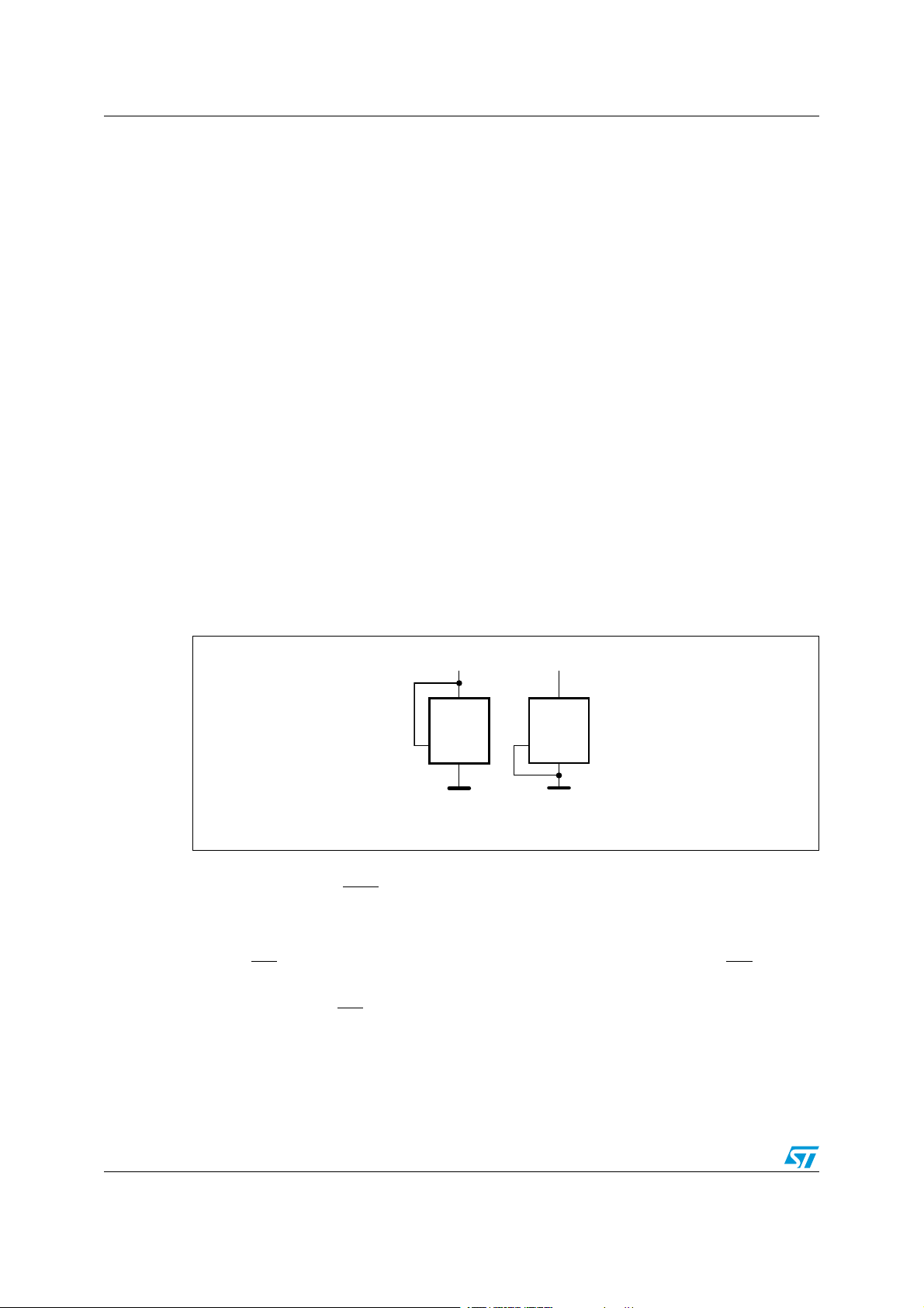
M24512-W M24512-R M24512-DR M24512-DF DC and AC parameters
AIB
"USLINECAPACITORP&
"USLINEPULLUPRESISTOR
K
)£#BUS
MASTER
-XXX
2
BUS
6
##
#
BUS
3#,
3$!
2
BUS
§#
BUS
NS
(ERE2
BUS
§#
BUS
NS
K½
P&
4HE2X#TIMECONSTANT
MUSTBEBELOWTHENS
TIMECONSTANTLINEREPRESENTED
ONTHELEFT
BUS
BUS
Figure 12. Maximum R
2
an I
C bus at maximum frequency fC = 400 kHz
Figure 13. Maximum R
2
an I
C bus at maximum frequency fC = 1MHz
value versus bus parasitic capacitance (C
bus
value versus bus parasitic capacitance C
bus
bus
bus
) for
) for
6
##
2
BU
§
S
#
BU
NS
"USLINEPULLUPRESISTORK
S
§
(ERE
NS
#
2
BUS
BUS
"USLINECAPACITORP&
4HE2
§#
TIMECONSTANT
BUS
MUSTBEBELOWTHENS
TIMECONSTANTLINEREPRESENTED
ONTHELEFT
BUS
)£#BUS
MASTER
3#,
3$!
2
BUS
#
BUS
-XXX
-36
Doc ID 16459 Rev 25 31/44
Page 32

DC and AC parameters M24512-W M24512-R M24512-DR M24512-DF
3#,
3$!/UT
3#,
3$!)N
$ATAVALID
T#,16 T#,18
T#($(
3TOP
CONDITION
T#($,
3TART
CONDITION
7RITECYCLE
T7
!)G
$ATAVALID
T1,1,
3$!)N
T#($,
3TART
CONDITION
T$8#(T#,$8
3$!
)NPUT
3$!
#HANGE
T#($( T$($,
3TOP
CONDITION
3TART
CONDITION
T8(8(
3#,
T#(#,
T$,#,
T#,#(
T8(8(
T8,8,
T8,8,
7#
T7,$,
T$(7(
Figure 14. AC waveforms
32/44 Doc ID 16459 Rev 25
Page 33

M24512-W M24512-R M24512-DR M24512-DF Package mechanical data
9 Package mechanical data
In order to meet environmental requirements, ST offers these devices in different grades of
ECOPACK
specifications, grade definitions and product status are available at: www.st.com.
ECOPACK
®
packages, depending on their level of environmental compliance. ECOPACK®
®
is an ST trademark.
Figure 15. TSSOP8 – 8-lead thin shrink small outline, package outline
1. Drawing is not to scale.
Table 18. TSSOP8 – 8-lead thin shrink small outline, package mechanical data
millimeters inches
Symbol
Typ. Min. Max. Typ. Min. Max.
(1)
A 1.200 0.0472
A1 0.050 0.150 0.0020 0.0059
A2 1.000 0.800 1.050 0.0394 0.0315 0.0413
b 0.190 0.300 0.0075 0.0118
c 0.090 0.200 0.0035 0.0079
CP 0.100 0.0039
D 3.000 2.900 3.100 0.1181 0.1142 0.1220
e 0.650 – – 0.0256 – –
E 6.400 6.200 6.600 0.2520 0.2441 0.2598
E1 4.400 4.300 4.500 0.1732 0.1693 0.1772
L 0.600 0.450 0.750 0.0236 0.0177 0.0295
L1 1.000 0.0394
α 0° 8° 0° 8°
1. Values in inches are converted from mm and rounded to four decimal digits.
Doc ID 16459 Rev 25 33/44
Page 34

Package mechanical data M24512-W M24512-R M24512-DR M24512-DF
SO-A
E1
8
ccc
b
e
A
D
c
1
E
h x 45˚
A2
k
0.25 mm
L
L1
A1
GAUGE PLANE
Figure 16. SO8N – 8 lead plastic small outline, 150 mils body width, package outline
1. Drawing is not to scale.
Table 19. SO8N – 8 lead plastic small outline, 150 mils body width, package data
millimeters inches
Symbol
Typ Min Max Typ Min Max
A 1.750 0.0689
A1 0.100 0.250 0.0039 0.0098
A2 1.250 0.0492
b 0.280 0.480 0.0110 0.0189
c 0.170 0.230 0.0067 0.0091
ccc 0.100 0.0039
D 4.900 4.800 5.000 0.1929 0.1890 0.1969
E 6.000 5.800 6.200 0.2362 0.2283 0.2441
E1 3.900 3.800 4.000 0.1535 0.1496 0.1575
e 1.270 0.0500
h 0.250 0.500 0.0098 0.0197
k 0°8° 0°8°
L 0.400 1.270 0.0157 0.0500
L1 1.040 0.0409
1. Values in inches are converted from mm and rounded to four decimal digits.
(1)
34/44 Doc ID 16459 Rev 25
Page 35

M24512-W M24512-R M24512-DR M24512-DF Package mechanical data
$
%
:7?-%E6
!
!
EEE
,
E B
$
,
%
,
0IN
+
Figure 17. UFDFPN8 (MLP8) - 8-lead ultra thin fine pitch dual flat no lead, package
outline
1. Drawing is not to scale.
2. The central pad (area E2 by D2 in the above illustration) is internally pulled to V
connected to any other voltage or signal line on the PCB, for example during the soldering process.
Table 20. UFDFPN8 (MLP8) 8-lead ultra thin fine pitch dual flat package no lead
. It must not be
SS
2 x 3 mm, data
millimeters inches
Symbol
Typ Min Max Typ Min Max
(1)
A 0.550 0.450 0.600 0.0217 0.0177 0.0236
A1 0.020 0.000 0.050 0.0008 0.0000 0.0020
b 0.250 0.200 0.300 0.0098 0.0079 0.0118
D 2.000 1.900 2.100 0.0787 0.0748 0.0827
D2 (rev MC) 1.200 1.600 0.0472 0.0630
E 3.000 2.900 3.100 0.1181 0.1142 0.1220
E2 (rev MC) 1.200 1.600 0.0472 0.0630
e 0.500 0.0197
K (rev MC) 0.300 0.0118
L 0.300 0.500 0.0118 0.0197
L1 0.150 0.0059
L3 0.300 0.0118
(2)
eee
1. Values in inches are converted from mm and rounded to four decimal digits.
2. Applied for exposed die paddle and terminals. Exclude embedding part of exposed die paddle from
measuring.
0.080 0.0031
Doc ID 16459 Rev 25 35/44
Page 36

Package mechanical data M24512-W M24512-R M24512-DR M24512-DF
8
AAA
7AFERBACKSIDE
$
%
3IDEVIEW
$ETAIL!
!
!
"UMPSSIDE
$ETAIL!
2OTATED
"UMP
EEE
!
3EATINGPLANE
#F?-%?6
B
BBB
:
:
8
CCC-
9
:
DDD-
8
9
:
:
2EFERENCE
E
E
'
&
E
E
2EFERENCE
Figure 18. M24512-DFCS6TP/K , WLCSP 8-bump wafer-level chip scale package
outline
1. Drawing is not to scale.
36/44 Doc ID 16459 Rev 25
Page 37

M24512-W M24512-R M24512-DR M24512-DF Package mechanical data
Table 21. M24512-DFCS6TP/K, WLCSP 8-bump wafer-level chip scale package
mechanical data
Symbol millimeters inches
Typ Min Max Typ Min Max
A 0.540 0.500 0.580 0.0213 0.0197 0.0228
A1 0.190 0.0075
A2 0.350 0.0138
b 0.270 0.0106
D 1.271 1.291 0.0500 0.0508
E 1.937 1.957 0.0763 0.0770
e 1.000 0.0394
e1 0.866 0.0341
e2 0.500 0.0197
e3 0.433 0.0170
F 0.202 0.0080
G 0.469 0.0185
N 8.000 0.3150
(1)
aaa 0.110 0.0043
bbb 0.110 0.0043
ccc 0.110 0.0043
ddd 0.060 0.0024
eee 0.060 0.0024
1. Values in inches are converted from mm and rounded to four decimal digits.
Doc ID 16459 Rev 25 37/44
Page 38

Part numbering M24512-W M24512-R M24512-DR M24512-DF
10 Part numbering
Table 22. Ordering information scheme
Example: M24512 W MN 6 T P /K
Device type
2
M24 = I
C serial access EEPROM
Device function
512 = 512 Kbit (64 x 8)
Device family
Blank: Without Identification page
-D: With additional Identification page
Operating voltage
W = V
R = V
= 2.5 V to 5.5 V
CC
= 1.8 V to 5.5 V
CC
F = VCC = 1.7 V to 5.5 V
Package
MN = SO8 (150 mil width)
DW = TSSOP8 (169 mil width)
(1)
(1)
MC = UFDFPN8 (MLP8)
CS = standard WLCSP
Device grade
6 = Industrial: device tested with standard test flow over –40 to 85 °C
Option
blank = standard packing
T = Tape and reel packing
Plating technology
®
P or G = ECOPACK
(2)
Process
(RoHS compliant)
/K = Manufacturing technology code
1. RoHS-compliant and halogen-free (ECOPACK2®)
2. The process letters apply to WLCSP devices only. The process letters appear on the device package
(marking) and on the shipment box. Please contact your nearest ST Sales Office for further information.
38/44 Doc ID 16459 Rev 25
Page 39

M24512-W M24512-R M24512-DR M24512-DF Revision history
11 Revision history
Date Revision Changes
Lead Soldering Temperature in the Absolute Maximum Ratings table
amended
29-Jan-2001 1.1
10-Apr-2001 1.2
16-Jul-2001 1.3 LGA8 Package given the designator “LA”
02-Oct-2001 1.4 LGA8 Package mechanical data updated
13-Dec-2001 1.5
12-Jun-2001 1.6 Document promoted to Full Datasheet
22-Oct-2003 2.0
02-Sep-2004 3.0
Write Cycle Polling Flow Chart using ACK illustration updated
LGA8 and SO8(wide) packages added
References to PSDIP8 changed to PDIP8, and Package Mechanical data
updated
LGA8 Package Mechanical data and illustration updated
SO16 package removed
Document becomes Preliminary Data
Test conditions for ILI, ILO, ZL and ZH made more precise
VIL and VIH values unified. tNS value changed
Table of contents, and Pb-free options added. Minor wording changes in
Summary Description, Power-On Reset, Memory Addressing, Write
Operations, Read Operations. V
(min) improved to –0.45V.
IL
LGA8 package is Not for New Design. 5V and -S supply ranges, and
Device Grade 5 removed. Absolute Maximum Ratings for V
(min) changed. Soldering temperature information clarified for RoHS
V
CC
(min) and
IO
compliant devices. Device grade information clarified. AEC-Q100-002
compliance. VIL specification unified for SDA, SCL and WC
22-Feb-2005 4.0
Initial delivery state is FFh (not necessarily the same as Erased).
LGA package removed, TSSOP8 and SO8N packages added (see
Package mechanical data section and Table 21: Ordering information
scheme).
Voltage range R (1.8V to 5.5V) also offered. Minor wording changes.
Test Conditions modified in Table 11: Input parameters and Note 2
Z
L
added.
I
CC
and I
values for VCC = 5.5V added to Table 12: DC characteristics
CC1
(voltage range W).
Note added to Table 12: DC characteristics (voltage range W).
Power On Reset paragraph specified.
max value modified in Table 14: 400 kHz AC characteristics and note 4
t
W
added. Plating technology changed in Table 21: Ordering information
scheme.
Resistance and capacitance renamed in Figure 6.
Doc ID 16459 Rev 25 39/44
Page 40

Revision history M24512-W M24512-R M24512-DR M24512-DF
Date Revision Changes
Power On Reset paragraph replaced by Section 2.6: Supply voltage
(VCC). Figure 4: Device select code added.
ECC (error correction code) and write cycling added and specified at 1
05-May-2006 5
16-Oct-2006 6
02-Jul-2007 7
16-Oct-2007 8
Million cycles.
added and I
I
CC0
specified over the whole voltage range in Ta b le 1 2
CC1
and Ta bl e 1 3 .
PDIP8 package removed. Packages are ECOPACK® compliant. Small
text changes.
M24256-BW and M24256-BR part numbers added.
Section 3.12: ECC (error correction code) and write cycling updated.
I
CC
and I
modified in Table 13: DC characteristics (voltage range R).
CC1
tW modified in Table 14: 400 kHz AC characteristics.
SO8Narrow package specifications updated (see Ta b l e 1 7 and
Figure 15). Blank option removed from below Plating technology in
Table 21: Ordering information scheme.
Section 2.6: Supply voltage (VCC) modified.
Section 3.12: ECC (error correction code) and write cycling modified.
JEDEC standard and European directive references corrected below
Table 7: Absolute maximum ratings.
Rise/fall time conditions modified for I
and VIH max modified in
CC
Table 12: DC characteristics (voltage range W) and Table 13: DC
characteristics (voltage range R)
Note 1 removed from Table 12: DC characteristics (voltage range W).
SO8W package specifications modified in Section 7: Package mechanical
data.
Table 23: Available M24256-BR, M24256-BW, M24256-BF products
(package, voltage range, temperature grade) and Table 26: Available
M24512-x products (package, voltage range, temperature grade) added.
Section 2.5: VSS ground added. Small text changes.
max changed and Note 1 updated to latest standard revision in
V
IO
Table 7: Absolute maximum ratings.
Note removed from Table 11: Input parameters.
min and VIL max modified in Table 13: DC characteristics (voltage
V
IH
range R).
Removed t
CH1CH2
, t
CL1CL2
and t
DH1DH2
, and added t
XL1XL2
, t
DL1DL2
and
Note 3 in Table 14: 400 kHz AC characteristics.
t
XH1XH2
, t
and Note 2 added to Table 15: 1 MHz AC characteristics.
XL1XL2
Figure 13: AC timings modified.
Package mechanical data inch values calculated from mm and rounded to
4 decimal digits (see Section 7: Package mechanical data).
40/44 Doc ID 16459 Rev 25
Page 41

M24512-W M24512-R M24512-DR M24512-DF Revision history
Date Revision Changes
1 MHz frequency introduced (M24512-HR root part number).
Section 2.6.3: Device reset modified.
Figure 5: I2C Fast mode (fC = 400 kHz): maximum Rbus value versus bus
parasitic capacitance (Cbus) modified, Figure 6: I2C Fast mode Plus (fC =
14-Dec-2007 9
27-Mar-2008 10
22-Apr-2008 11
22-Dec-2008 12
21-Jan-2009 13
05-Jun-2009 14
16-Jun-2009 15 Part numbers updated in cover page header.
1 MHz): maximum Rbus value versus bus parasitic capacitance (Cbus)
added.
moved from Ta bl e 1 1 to Ta bl e 1 4 . ILO test conditions modified in
t
NS
Ta ble 12 .
Table 13: DC characteristics (voltage range R) and Table 15: 1 MHz AC
characteristics modified. Small text changes.
Small text changes. M24256-BHR root part number added.
Section 2.6.3: Device reset on page 9 updated.
Figure 6: I2C Fast mode Plus (fC = 1 MHz): maximum Rbus value versus
bus parasitic capacitance (Cbus) on page 10 updated.
Caution removed in Section 3.12: ECC (error correction code) and write
cycling.
M24512-W and M24256-BW offered in the device grade 3 option
(automotive temperature range):
– Table 8: Operating conditions (voltage range W),
– Table 12: DC characteristics (voltage range W),
– /AB Process letters added to Table 21: Ordering information scheme,
– Table 23: Available M24256-BR, M24256-BW, M24256-BF products
(package, voltage range, temperature grade) and
– Table 26: Available M24512-x products (package, voltage range,
temperature grade) updated accordingly).
Small text changes.
WLCSP package added (see Figure 3: WLCSP connections (top view,
marking side, with balls on the underside) and Section 7: Package
mechanical data).
M24256-BF part number added (V
= 1.7 V to 5.5 V voltage range
CC
added, see Ta bl e 1 0 , Tab l e 1 4 and Table 23).
test conditions modified in Table 12: DC characteristics (voltage
I
CC1
range W), Table 13: DC characteristics (voltage range R) and Tab l e 1 4 :
DC characteristics (voltage range F).
M24512-DR part number and Identification page feature added.
Command replaced by instruction in the whole document.
UFDFPN8 added.
Figure 6 updated.
Section 2.6.2: Power-up conditions and Section 2.6.3: Device reset
updated.
t
CLQX
t
CLQX
and t
and t
updated in Ta bl e 1 4 , Note 6 and Note 8 added.
CLQV
updated in Ta b le 15, Note 5 and Note 8 added.
CLQV
Section 8: Part numbering updated.
Reference to the SURE program removed in Section 5: Maximum rating.
Previous 1 MHz M24512-HR and M24512-BHR devices replaced by new
M24512-R and M24256-BR (process letter K).
Doc ID 16459 Rev 25 41/44
Page 42

Revision history M24512-W M24512-R M24512-DR M24512-DF
Date Revision Changes
I
added to Table 8: Operating conditions (voltage range W).
OL
20-Aug-2009 16
13-Oct-2009 17
Note 1 and I
W); Note 2 and ICC modified in Table 13: DC characteristics (voltage
range R);
Datasheet split to leave only devices with 512 Kbit capacity.
Figure 4: Device select code and Figure 5: I2C Fast mode (fC = 400 kHz):
maximum Rbus value versus bus parasitic capacitance (Cbus) updated.
VIO max modified in Table 7: Absolute maximum ratings.
modified in Table 12: DC characteristics (voltage range W), Ta bl e 1 3 :
V
IH
DC characteristics (voltage range R) and Table 14: DC characteristics
(voltage range F).
In Table14: 400kHz AC characteristics and Table 15: 1 MHz AC
characteristics:
–t
DL1DL2
–t
CHDX
–t
XH1XH2
– Notes modified
Figure 13: AC timings modified.
modified in Table 12: DC characteristics (voltage range
CC
changed to t
changed to t
and t
QL1QL2
CHDL
values removed
XL1XL2
05-Nov-2009 18
01-Jun-2010 19
28-Sep-2010 20
21-Dec-2010 21
Section 3.10: Write Identification Page (M24512-DR only) corrected.
Section 3.18: Read Identification Page (M24512-D only) clarified.
Clarified cover page.
Section 1: Description inserted paragraph clarifying Identification Page.
Section 3.1: Start condition clarified.
Section 3.7: Write operations clarified.
Section 3.10: Write Identification Page (M24512-DR only) clarified.
Section 3.18: Read Identification Page (M24512-D only) paragraph
updated.
Table 7: Absolute maximum ratings updated.
Table 10: AC test measurement conditions updated.
Table 12: DC characteristics (voltage range W) updated.
Table 13: DC characteristics (voltage range R) updated.
Table 14: DC characteristics (voltage range F) table deleted.
Re-ordered Features content.
WLCSP package information added in Figure 3.
Text updated in Section 3.10, Section 3.18.
Updated Figure 13.
Added Figure 18, Ta bl e 2 0 .
Updated Features, Section 1: Description, Section 3.12: ECC (error
correction code) and write cycling, title of sections 3.18 and 3.19,
Table 12: DC characteristics (voltage range W), Table 13: DC
characteristics (voltage range R), Table 14: 400 kHz AC characteristics
and Table 15: 1 MHz AC characteristics, Figure 17: UFDFPN8 (MLP8) 8-
lead ultra thin fine pitch dual flat package no lead 2 x 3 mm, outline.
Added Caution under Figure 3.
42/44 Doc ID 16459 Rev 25
Page 43

M24512-W M24512-R M24512-DR M24512-DF Revision history
Date Revision Changes
Updated Ta ble 7 , Ta bl e 1 3 , Tab l e 1 6 and Tab l e 1 7 .
(2)
to Ta bl e 1 4 .
31-Jan-2011 22
Added note
Deleted Table 22: Available M24512-W and M24512-R products
(package, voltage range, temperature grade) and Table 23: Available
M24512-DR products (package, voltage range, temperature grade).
– Deleted reference “M24512-DR” and inserted reference “M24512-DF”.
– Updated data regarding package UFDFPN8.
– Updated Section 1: Description.
– Added Figure 4 and updated title of Figure 3.
value in Table 7: Absolute maximum ratings, note
ESD
01-Mar-2012 23
– Updated V
under Ta b le 1 3 and ICC value in Ta bl e 1 4 .
– Added Table 10: Operating conditions (voltage range F) and Table 15:
DC characteristics (voltage range F).
– Added values t
WLDL
and t
DHWH
and Table 17: 1 MHz AC characteristics .
–Replaced Figure 14.
12-Apr-2012 24 Updated Section 1: Description.
Datasheet split into:
– M24512-125 datasheet for automotive products (range 3),
– M24512-W M24512-R M24512-DR M24512-DF for standard products
(range 6, this datasheet rev 25).
Deleted:
–SO8W package
– UFDFPN8 (MLP8): MB version package
– WLCSP (KA die) dimensions
25-Jun-2012 25
Added:
– Reference M24512-DR
– Table 11: Cycling performance by groups of four bytes
– Table 12: Memory cell data retention
Updated:
– Figure 12: Maximum R
– Figure 13: Maximum R
for an I
for an I
2
C bus at maximum frequency fC = 400 kHz
2
C bus at maximum frequency fC = 1MHz
value versus bus parasitic capacitance (C
bus
value versus bus parasitic capacitance C
bus
(1)
in Table 16: 400 kHz AC characteristics
bus
bus
)
)
Doc ID 16459 Rev 25 43/44
Page 44

M24512-W M24512-R M24512-DR M24512-DF
Please Read Carefully:
Information in this document is provided solely in connection with ST products. STMicroelectronics NV and its subsidiaries (“ST”) reserve the
right to make changes, corrections, modifications or improvements, to this document, and the products and services described herein at any
time, without notice.
All ST products are sold pursuant to ST’s terms and conditions of sale.
Purchasers are solely responsible for the choice, selection and use of the ST products and services described herein, and ST assumes no
liability whatsoever relating to the choice, selection or use of the ST products and services described herein.
No license, express or implied, by estoppel or otherwise, to any intellectual property rights is granted under this document. If any part of this
document refers to any third party products or services it shall not be deemed a license grant by ST for the use of such third party products
or services, or any intellectual property contained therein or considered as a warranty covering the use in any manner whatsoever of such
third party products or services or any intellectual property contained therein.
UNLESS OTHERWISE SET FORTH IN ST’S TERMS AND CONDITIONS OF SALE ST DISCLAIMS ANY EXPRESS OR IMPLIED
WARRANTY WITH RESPECT TO THE USE AND/OR SALE OF ST PRODUCTS INCLUDING WITHOUT LIMITATION IMPLIED
WARRANTIES OF MERCHANTABILITY, FITNESS FOR A PARTICULAR PURPOSE (AND THEIR EQUIVALENTS UNDER THE LAWS
OF ANY JURISDICTION), OR INFRINGEMENT OF ANY PATENT, COPYRIGHT OR OTHER INTELLECTUAL PROPERTY RIGHT.
UNLESS EXPRESSLY APPROVED IN WRITING BY TWO AUTHORIZED ST REPRESENTATIVES, ST PRODUCTS ARE NOT
RECOMMENDED, AUTHORIZED OR WARRANTED FOR USE IN MILITARY, AIR CRAFT, SPACE, LIFE SAVING, OR LIFE SUSTAINING
APPLICATIONS, NOR IN PRODUCTS OR SYSTEMS WHERE FAILURE OR MALFUNCTION MAY RESULT IN PERSONAL INJURY,
DEATH, OR SEVERE PROPERTY OR ENVIRONMENTAL DAMAGE. ST PRODUCTS WHICH ARE NOT SPECIFIED AS "AUTOMOTIVE
GRADE" MAY ONLY BE USED IN AUTOMOTIVE APPLICATIONS AT USER’S OWN RISK.
Resale of ST products with provisions different from the statements and/or technical features set forth in this document shall immediately void
any warranty granted by ST for the ST product or service described herein and shall not create or extend in any manner whatsoever, any
liability of ST.
ST and the ST logo are trademarks or registered trademarks of ST in various countries.
Information in this document supersedes and replaces all information previously supplied.
The ST logo is a registered trademark of STMicroelectronics. All other names are the property of their respective owners.
© 2012 STMicroelectronics - All rights reserved
STMicroelectronics group of companies
Australia - Belgium - Brazil - Canada - China - Czech Republic - Finland - France - Germany - Hong Kong - India - Israel - Italy - Japan -
Malaysia - Malta - Morocco - Philippines - Singapore - Spain - Sweden - Switzerland - United Kingdom - United States of America
www.st.com
44/44 Doc ID 16459 Rev 25
 Loading...