

Page 1

M22101
M22102
4 X 4 X 2 CROSSPOINT SWITCHES
WITH CONTROLMEMORY
.LOW ON RESISTANCE– 75Ω TYPAT
VDD=12V
.”BUILT-IN” LATCHED INPUTS
.LARGE ANALOG SIGNALCAPACITY±V
DD
/2
.10 MHz SWITCH BANDWITH
.MATCHED SWITCHCHARACTERISTICS
.∆ RON = 8 Ω TYP, AT V
DD
=12V
.HIGH LINEARITY – 0.25 % DISTORTION TYP,
AT f = 1 kHz, VIN= 5 V, VDD-VSS= 10 V AND
RI = 1 Ω
.STANDARD CMOS NOISEIMMUNITY
DESCRIPTION
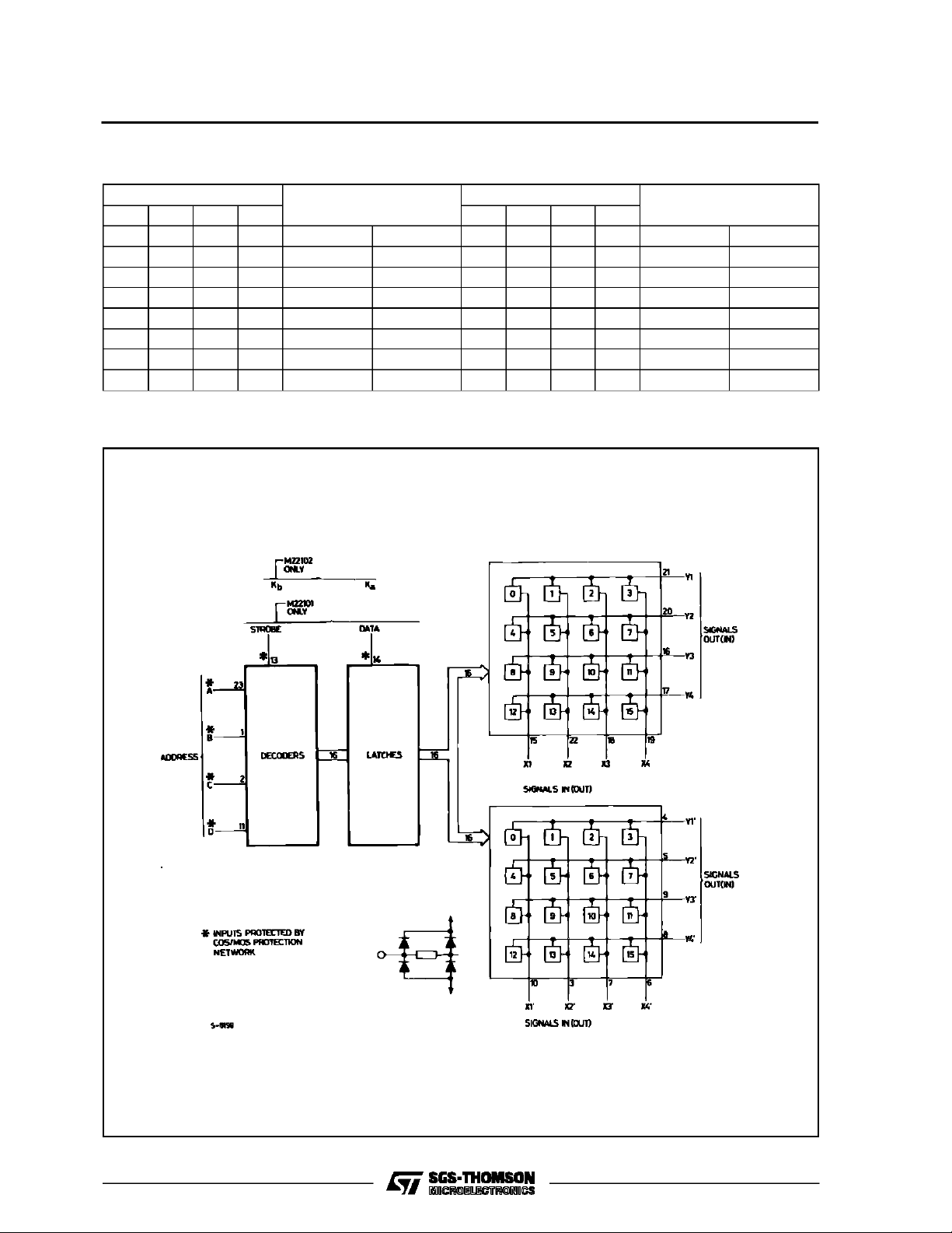
TheM22101 and M22102 crosspoint switches con-
sist of 4 x 4 x 2 arrays of crosspoints (transmission
gates), 4-line to 16-linedecoders, and 16 latchcircuits.Anyone ofthe sixteen crosspoint pairscan be
selected by applying the appropriate four-line addressandanynumber ofcrosspoint pairscanbeON
simultaneously. Corresponding crosspointsin each
arrayare turned on and OFFsimultaneously, also.
In the M22101, the selected crosspoint pair can be
turnedon oroff by applyingalogical ONEor ZERO,
respectively, to the data input,and applying aONE
to the strobe input. When the device is”power-up”,
the state of the16 switches is indeterminate.
Therefore all switches mustbe turned offby putting
the strobe hight,data-in-low, and theaddressing all
switches in succession.
The selected pair of crosspoints in the M22102 is
turnedon by applying a logical ONE to the Ka(set)
input whilealogical ZEROis on theKb(reset) input,
and turned off by applying a logical ONE to the K
input while a logical ZEROis on theKainput.In this
respectthecontrol latches oftheM22102 aresimilar
to SET/RESET flip-flops. They differ, however, in
thatthe simultaneousapplication of ONEstothe K
and Kbinputs turns off (resets) all crosspoints. All
crosspoints in both devices must be turned off as
VDDis applied.
B1
(PlasticPackage)
ORDER CODES :
M22XXX B1 M22XXX F1
(CeramicPackage)
F1
b
a
PIN CONNECTIONS
September 1988
1/8
Page 2
M22101/M22102
ABSOLU TE M AXIMU M R AT ING
Symbol Parameter Value Unit
V
DD
V
P
T
T
Stressesabove thoselistedunder ”Absolute Maximum Ratings”maycause permanent damagetothedevice. Thisisastressratingonlyand functional
operation ofthe device at these or any otherconditions above thoseindicatedintheoperational sections of thisspecification isnot implied.Exposure
to absolute maximumratingconditions forexternal periods mayaffect device reliability.
RECO MM ENDED OPERAT I N G CO NDI TIONS
Symbol Parameter Value Unit
V
V
T
Supply Voltage: Ceramic Type
Plastic Type
Input Voltage -0.5 to VDD+ 0.5 V
i
I
DC Input Current (any one input) ± 10 mA
I
Total Power Dissipation (per package)
tot
-0.5 to +20
-0.5 to +18
200
Dissipation per Output Transistor
for Top = Full Package Temperature Range
Operating Temperature: Ceramic Type
op
Plastic Type
Storage Temperature -65 to +150
stg
Supply Voltage: Ceramic Type
DD
Plastic Type
Input Voltage 0 to V
I
Operating Temperature: Ceramic Type
op
Plastic Type
100
-55 to +125
-40 to +85
3to18
3to15
DD
-55 to +125
-40 to +85
V
V
mW
mW
o
C
o
C
o
C
V
V
V
o
C
o
C
CONT RO L TRUT H TABLE FOR M22101
Function
ABCD
Switch-on 1 1 1 1 1 1 (X4 Y4) & (X4’ Y4’)
Switch-off 1 1 1 1 1 0 (X4 Y4) & (X4’ Y4’)
No Change X X X X 0 X XXXX
Note: 1=High,0 = Low, X= Don’tCare
Address
Strobe Data Select
CONT RO L TRUT H TABLE FOR M22102
Function
ABCD
Switch-on 1 1 1 1 1 0 (X4 Y4) & (X4’ Y4’)
Switch-off 1 1 1 1 0 1 (X4 Y4) & (X4’ Y4’)
All Switch-off X X X X 1 1 All
No Change X X X X 0 0 XXXX
Note: 1=High,0 = Low, X= Don’tCare
Address
Strobe Data Select
2/8
Page 3
DECODER TRUTH TABLE
M22101/M22102
Address
ABCD ABCD
0000 X1Y1 X1’Y1’ 0001 X1Y3 X1’Y3’
1000 X2Y1 X2’Y1’ 1001 X2Y3 X2’Y3’
0100 X3Y1 X3’Y1’ 0101 X3Y3 X3’Y3’
1100 X4Y1 X4’Y1’ 1101 X4Y3 X4’Y3’
0010 X1Y2 X1’Y2’ 0011 X1Y4 X1’Y4’
1010 X2Y2 X2’Y2’ 1011 X2Y4 X2’Y4’
0110 X3Y2 X3’Y2’ 0111 X3Y4 X3’Y4’
1110 X4Y2 X4’Y2’ 1111 X4Y4 X4’Y4’
Select
Address
Select
FUNCTIONAL AND BLOCK DIAGRAM
3/8
Page 4

M22101/M22102
STATI C ELE CT RIC AL CHA R ACTER I STI CS (ove r recom mended oper ating c onditio ns)
Test Conditios Value
Symbol Parameter
V
(V)
V
I
(V)
T
DD
*25
LOW
Min. Max. Min. Typ. Max. Min. Max.
o
CT
CROSSPOINT
I
L
Quiescent
Supply
Current
F1
5 0.04 5 150
10 0.04 10 300
15 0.04 20 600
20 0.08 100 3000
5 0.04 20 150
B1
10 0.04 40 300
15 0.04 80 600
ON
On
Resistance
F1 Any Switch
R
5 450 225 1250 1625
10 135 85 180 230
12 100 75 135 175
15 70 65 95 125
5 1000 225 1250 1440
B1 V
= 0 to V
IS
DD
10 145 85 180 205
12 110 75 135 155
15 75 65 95 110
∆ON Resistance ∆R
(Between any two
channels)
ON
535
10 20
12 18
15 15
OFF
Channel
Leakage
Current
F1
B1 0/15 15 ±0.3 ±10
All Switch
OFF
0/18 18 ±0.1 ±10
-3
±0.1•±1
-3
±0.3 ±1
CONTROL
V
IL
Input Low
Voltage
OFF Switch
I
< 0.2 µA
L
5 1.5 1.5 1.5
10 3 3 3
15 4 4 4
IH
Input High
V
Voltage
Input
I
I
Current
C
• Determined byminimum feasible leakagemeasurement forautomatic testing
*T
LOW
*T
HIGH
TheNoiseMargin for both ”1” and”0” levelis: 1Vmin.withVDD=5V, 2V min.with VDD=10 V, 2.5 Vmin. withVDD=15V
Input Capacitance Any Input 5 7.5 pF
I
=-55oCforHCC device:-40oC for HCF device.
=+125oCforHCC device:+85oC for HCFdevice.
F1
B1 0/15 15 ±0.3 ±10
ON Switch
see R
ON
Characteristics
Any Control
Input
5 3.5 3.5 3.5
10 7 7 7
15 11 11 11
0/18 18 ±0.1 ±10-5±0.1 ±1
-5
±0.3 ±1
HIGH
*
Unit
µA
Ω
Ω
µA
V
V
µA
4/8
Page 5

M22101/M22102
DYNAMIC ELECTRICAL CHARACTERISTICS (T
=25oC, CL=50pF,RL= 200 KΩ,
amb
typic al temperatur e coeff i c ent for all VDDvalues is 03 %/oC, all input ri s e and fall tim es = 20 ns)
Symbol Parameter
t
t
t
t
PHL
PLH
PHL
PLH
Propagation Delay Time Address or Strobe
Inputs to Output
Propagation Delay Time Across Crosspoint 20 ns
Minimum Strobe Pulse Width 80 ns
Test Conditions Value
(V) Min. Typ. Max.
V
DD
R
=10KΩ
L
CL=50pF
12
200
Unit
ns
5/8
Page 6

M22101/M22102
Plastic DIP24 (0.25) MECHANICAL DATA
DIM.
MIN. TYP. MAX. MIN. TYP. MAX.
a1 0.63 0.025
b 0.45 0.018
b1 0.23 0.31 0.009 0.012
b2 1.27 0.050
D 32.2 1.268
E 15.2 16.68 0.598 0.657
e 2.54 0.100
e3 27.94 1.100
F 14.1 0.555
I 4.445 0.175
L 3.3 0.130
mm inch
6/8
P043A
Page 7

Ceramic DIP24 MECHANICAL DATA
M22101/M22102
DIM.
MIN. TYP. MAX. MIN. TYP. MAX.
A 32.3 1.272
B 13.05 13.36 0.514 0.526
C 3.9 5.08 0.154 0.200
D 3 0.118
E 0.5 1.78 0.020 0.070
e3 27.94 1.100
F 2.29 2.79 0.090 0.110
G 0.4 0.55 0.016 0.022
I 1.17 1.52 0.046 0.060
L 0.22 0.31 0.009 0.012
M 1.52 2.49 0.060 0.098
N1
P 15.4 15.8 0.606 0.622
Q 5.71 0.225
4° (min.), 15° (max.)
mm inch
P058C
7/8
Page 8

M22101/M22102
Information furnishedis believed to be accurate and reliable. However, SGS-THOMSON Microelectronicsassumes no responsability for the
consequences of useof suchinformation nor for any infringement of patents or other rights of third parties which may results from its use. No
license is granted byimplication or otherwiseunder any patentor patentrights ofSGS-THOMSON Microelectronics.Specificationsmentioned
in this publication are subjectto changewithout notice. This publication supersedes andreplaces all information previouslysupplied.
SGS-THOMSON Microelectronicsproducts are not authorized foruse ascritical componentsin life supportdevices or systems without express
written approval of SGS-THOMSON Microelectonics.
1994SGS-THOMSON Microelectronics- All Rights Reserved
Australia -Brazil - France - Germany - Hong Kong - Italy - Japan - Korea - Malaysia - Malta -Morocco - The Netherlands-
Singapore -Spain - Sweden- Switzerland - Taiwan - Thailand- UnitedKingdom - U.S.A
SGS-THOMSON Microelectronics GROUP OFCOMPANIES
8/8
 Loading...