

Page 1
Date:- 2 Nov, 2001
WESTCODE
Fast Recovery Diode
Types M1583VC400 to M1583VC450
Absolute Maximum Ratings
VOLTAGE RATINGS
V
RRM
V
RSM
I
F(AV)
I
F(AV)
I
F(AV)
I
F(RMS)
I
F(d.c.)
I
FSM
I
FSM2
I2tI
I2t
T
HS
T
stg
Repetitive peak reverse voltage, (note 1) 4000-4500 V
Non-repetitive peak reverse voltage, (note 1) 4100-4600 V
OTHER RATINGS
Mean forward current, T
Mean forward current. T
Mean forward current. T
Nominal RMS forward current, T
D.C. forward current, T
Peak non-repetitive surge tp=10ms, VRM=0.6V
Peak non-repetitive surge tp=10ms, V
2
t capacity for fusing tp=10ms, VRM=0.6V
2
t capacity for fusing tp=10ms, V
I
Operating temperature range -40 to +150 °C
Storage temperature range -40 to +150 °C
(note 6)
=55°C, (note 2) 1583 A
sink
=100°C, (note 2) 1030 A
sink
=100°C, (note 3) 624 A
sink
=25°C, (note 2) 2963 A
sink
=25°C, (note 4) 2569 A
sink
, (note 5) 24.8 kA
RRM
≤
10V, (note 5)
RM
, (note 5) 3.08×10
RRM
≤
10V, (note 5)
RM
Data Sheet Issue:- 1
MAXIMUM
LIMITS
MAXIMUM
LIMITS
27.3 kA
6
3.73×10
6
UNITS
UNITS
A2s
A2s
Notes:-
1)
De-rating factor of 0.13% per °C is applicable for Tj below 25°C.
2)
Double side cooled, single phase; 50Hz, 180° half-sinewave.
3)
Single side cooled, single phase; 50Hz, 180° half-sinewave.
4)
Double side cooled.
5)
Half-sinewave, 150°C Tj initial.
Data Sheet. Types M1583VC400 to M1583VC450 Issue 1 Page 1 of 11 November, 2001
Page 2
WESTCODE
Positive development in power electronics
Characteristics
M1583VC400 to M1583VC450
PARAMETER MIN. TYP. MAX. TEST CONDITIONS
V
V
r
S
Maximum peak forward voltage - - 2.8 IFM=2000A V
FM
Threshold voltage - - 1.693 V
0
Slope resistance - - 0.525
(Note 1)
UNITS
m
- - 110 di/dt = 1000A/µs
V
I
Q
Q
I
t
R
RRM
rm
rr
Maximum forward recovery voltage
FRM
Peak reverse current - - 150 Rated V
Reverse Recovery Charge - 2000 - µC
rr
Recovered charge, 50% Chord - 1100 1500 µC
ra
Reverse Recovery Current - 500 - A
- - 70 di/dt = 1000A/µs, Tj=25°C
RRM
I
=1000A, tp=500µs, di/dt=200A/µs,
FM
=50V, 50% Chord.
V
r
Reverse recovery time, 50% Chord - 5.0 -
- - 0.016 Double side cooled
Thermal resistance, junction to heatsink
th(j-hs)
- - 0.032 Single side cooled
V
mA
µs
K/W
F Mounting force 27 - 34 kN
W
Weight - 1000 - g
t
Notes:-
1) Unless otherwise indicated T
=150°C.
j
Ω
Introduction
The M1583VC400-450 fast recovery diode range has controlled reverse recovery characteristics.
Devices with a suffix code (2 letter or letter/digit/letter combination) added to their generic code are not
necessarily subject to the conditions and limits contained in this report.
Data Sheet. Types M1583VC400 to M1583VC450 Issue 1 Page 2 of 11 November, 2001
Page 3
WESTCODE
Notes on Ratings and Characteristics
1.0 Voltage Grade Table
Positive development in power electronics
M1583VC400 to M1583VC450
Voltage Grade V
40 4000 4100 2000
42 4200 4300 2040
44 4400 4500 2080
45 4500 4600 2100
2.0 De-rating Factor A blocking voltage de-rating factor of 0.13% per °C is applicable to this device for Tj below 25°C.
3.0 ABCD Constants These constants (applicable only over current range of VF characteristic in Figure 1) are the coefficients of
the expression for the forward characteristic given below:
RRM
(V)
)ln(
where IF = instantaneous forward current.
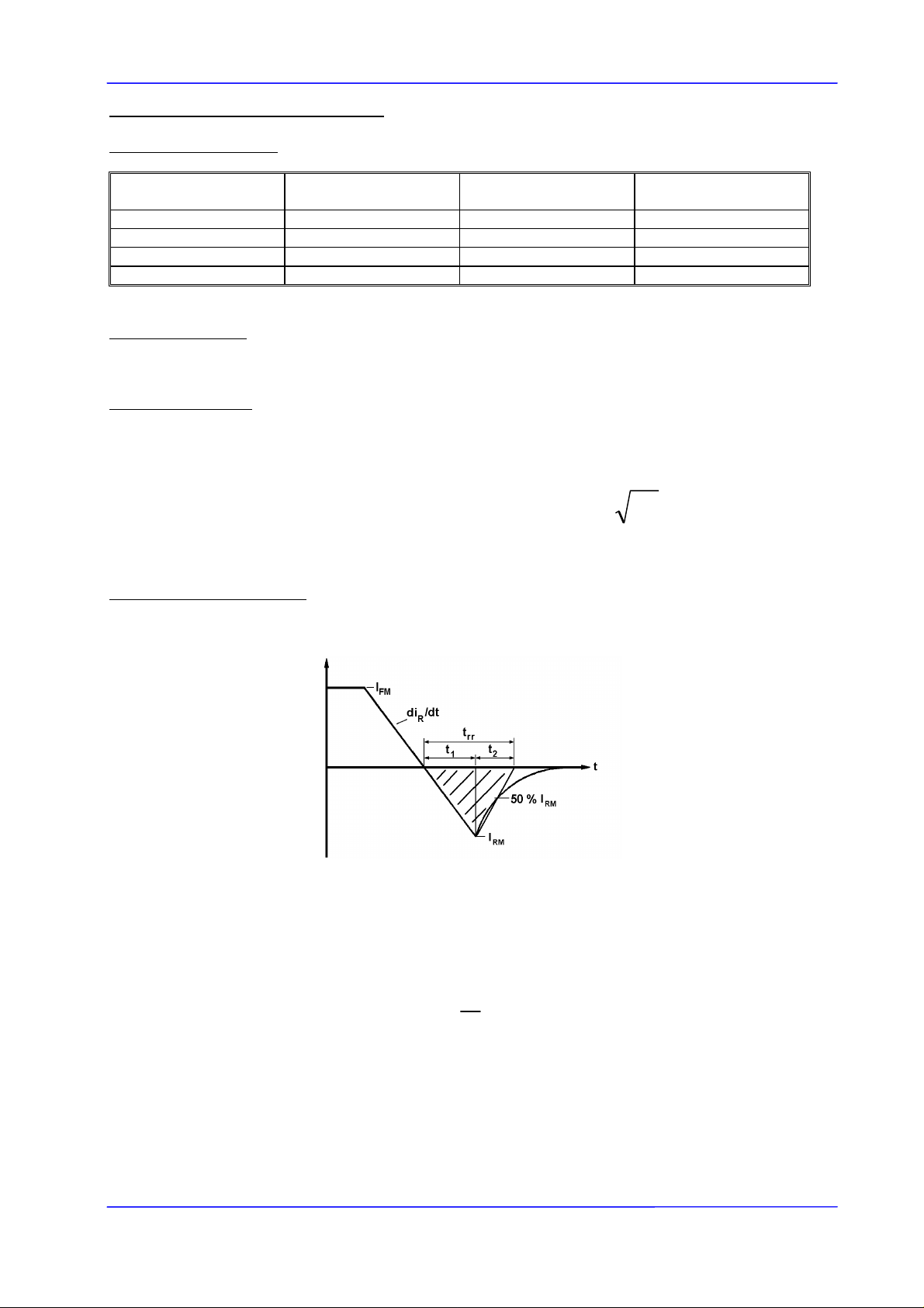
4.0 Reverse recovery ratings (i) Qra is based on 50% Irm chord as shown in Fig.(a) below.
V
RSM
(V)
IDICIBAV
⋅+⋅+⋅+=
FFFF
V
dc
R
(V)
(ii) Qrr is based on a 150µs integration time.
s
µ
150
I.e.
(iii)
Data Sheet. Types M1583VC400 to M1583VC450 Issue 1 Page 3 of 11 November, 2001
=
FactorK
dtiQ
.
rrrr
∫
0
t
1
=
t
2
Page 4

WESTCODE
)
5.0 Reverse Recovery Loss
The following procedure is recommended for use where it is necessary to include reverse recovery loss.
From waveforms of recovery current obtained from a high frequency shunt (see Note 1) and reverse
voltage present during recovery, an instantaneous reverse recovery loss waveform must be constructed.
Let the area under this waveform be E joules per pulse. A new sink temperature can then be evaluated
from:
Positive development in power electronics
M1583VC400 to M1583VC450
[]
Where k = 0.2314 (°C/W)/s
E
= Area under reverse loss waveform per pulse in joules (W.s.)
f
= Rated frequency in Hz at the original sink temperature.
R
The total dissipation is now given by:
This device has a low reverse recovered charge and peak reverse recovery current. When measuring the
charge, care must be taken to ensure that:
amplitude forward current.
to avoid overloading the internal amplifiers by the relatively high amplitude forward current signal.
= d.c. thermal resistance (°C/W)
th(J-Hs
fEWW
originaltot
NOTE 1 - Reverse Recovery Loss by Measurement
(a) AC coupled devices such as current transformers are not affected by prior passage of high
(b) A suitable, polarised, clipping circuit must be connected to the input of the measuring oscilloscope
)()(
⋅+=
⋅+⋅−=
RfkETT
−
HsJthMAXJSINK
)()(
(c) Measurement of reverse recovery waveform should be carried out with an appropriate critically
damped snubber, connected across diode anode to cathode. The formula used for the calculation of this
snubber is shown below:
2
R
Where: Vr= Commutating source voltage
4
V
⋅=
C
R = Snubber resistance
r
di
C
⋅
dt
S
= Snubber capacitance
S
Data Sheet. Types M1583VC400 to M1583VC450 Issue 1 Page 4 of 11 November, 2001
Page 5

WESTCODE
6.0 Computer Modelling Parameters
6.1 Device Dissipation Calculations
Positive development in power electronics
M1583VC400 to M1583VC450
4
oo
I
=
AV
2
Where Vo = 1.693V, rs = 0.525m
= form factor (normally unity for fast diode applications)
ff
T
∆
W
The forward characteristic I
(i) the well established V
((iiii))
=
AV
a set of constants A, B, C, and D forming the coefficients of the representative equation for V
R
th
−=∆
TTT
)(
6.2 Calculation of V
terms of I
given below:
F
HsMAXj
using ABCD Coefficients
F
Vs VF, on Fig. 1 is represented in two ways;
F
and rs tangent used for rating purposes and
0
22
2
rff
⋅⋅
s
Ω
WrffVV
⋅⋅⋅++−
AVs
IDICIBAV
)ln(
⋅+⋅+⋅+=
FFFF
in
F
The constants, derived by curve fitting software, are given in this report for hot characteristics. The
resulting values for V
that plotted.
agree with the true device characteristic over a current range, which is limited to
F
125°C Coefficients
A
B
C
D
0.734962026
0.04937503
0.162339×10
0.03052379
-3
Data Sheet. Types M1583VC400 to M1583VC450 Issue 1 Page 5 of 11 November, 2001
Page 6

WESTCODE
Positive development in power electronics
M1583VC400 to M1583VC450
Curves
Figure 1 – Forward characteristics of Limit device Figure 2 – Maximum forward recovery voltage
(A)
FM
10000
150°C
1000
(V)
FRM
1000
150°C
25°C
100
Instantaneous forward current - I
100
0123456
Maximum instantaneous forward voltage - V
Figure 3 - Recovered charge, Q
10000
M1583VC400-450
Issue 1
Tj = 150°C
(µC)
rr
1000
M1583VC400-450
rr
Issue 1
2000A
1500A
1000A
500A
10
Maximum forward recovery voltage - V
M1583VC400-450
Issue 1
1
(V)
FM
10 100 1000 10000
Rate of rise of forward current - di/dt (A/µs)
Figure 4 - Recovered charge, Qra (50% chord)
10000
M1583VC400-450
(µC)
ra
Issue 1
Tj = 150°C
1000
2000A
1500A
1000A
500A
Total recovered charge - Q
100
10 100 1000 10000
Commutation rate - di/dt (A/µs)
Data Sheet. Types M1583VC400 to M1583VC450 Issue 1 Page 6 of 11 November, 2001
Recovered charge - Q
100
10 100 1000 10000
Commutation rate - di/dt (A/µs)
Page 7

WESTCODE
Positive development in power electronics
M1583VC400 to M1583VC450
Figure 5 - Maximum reverse current, I
10000
(A)
rm
1000
Reverse recovery current - I
M1583VC400-450
100
10 100 1000 10000
Commutation rate - di/dt (A/µs)
rm
2000A
1500A
1000A
500A
Tj = 150°C
Issue 1
Figure 6 - Maximum recovery time, trr (50% chord)
10
(µs)
rr
Recovery time - t
1
10 100 1000 10000
Commutation rate - di/dt (A/µs)
2000A
1500A
1000A
500A
Tj = 150°C
M1583VC400-450
Issue 1
Figure 7 – Reverse recovery energy per pulse Figure 8 - Sine wave energy per pulse
10
M1583VC400-450
Issue 1
Tj = 150°C
V
= 67% V
RM
Snubber value
6.8
0.5µF
(mJ)
r
Energy per pulse - E
1
10 100 1000 10000
RRM
Ω
2000A
1500A
1000A
500A
Commutation rate - di/dt (A/µs)
1.00E+03
4kA
1.00E+02
1.00E+01
Energy per pulse (J)
1.00E+00
1.00E-01
1.00E-05 1.00E-04 1.00E-03 1.00E-02
3kA
2kA
1kA
500A
Pulse width (s)
M1583VC400-450
Tj = 150°C
Issue 1
Data Sheet. Types M1583VC400 to M1583VC450 Issue 1 Page 7 of 11 November, 2001
Page 8

WESTCODE
Positive development in power electronics
M1583VC400 to M1583VC450
Figure 9 - Sine wave frequency vs. pulse width Figure 10 - Sine wave frequency vs. pulse width
1.00E+05
1.00E+04
1.00E+03
Frequency (Hz)
1kA
2kA
3kA
4kA
500A
M1583VC400-450
Issue 1
100% Duty Cycle
THs = 55°C
1.00E+05
1.00E+04
1.00E+03
Frequency (Hz)
500A
1kA
2kA
3kA
4kA
M1583VC400-450
100% Duty Cycle
Issue 1
THs = 85°C
1.00E+02
1.00E+01
1.00E-05 1.00E-04 1.00E-03 1.00E-02
Pulse width (s)
Figure 11 - Square wave frequency vs pulse width
1.00E+05
1.00E+04
1.00E+03
Frequency (Hz)
1kA
2kA
3kA
4kA
M1583VC400-450
Issue 1
di/dt =100A/µs
THs=55°C
100% Duty Cycle
1.00E+02
1.00E+01
1.00E-05 1.00E-04 1.00E-03 1.00E-02
Pulse width (s)
Figure 12 - Square wave frequency vs pulse width
1.00E+05
1.00E+04
1.00E+03
Frequency (Hz)
500A
100% Duty Cycle
1kA
2kA
3kA
4kA
M1583VC400-450
Issue 1
di/dt =500A/µs
THs = 55°C
1.00E+02
1.00E+01
1.00E-05 1.00E-04 1.00E-03 1.00E-02
Pulse width (s)
Data Sheet. Types M1583VC400 to M1583VC450 Issue 1 Page 8 of 11 November, 2001
1.00E+02
1.00E+01
1.00E-05 1.00E-04 1.00E-03 1.00E-02
Pulse width (s)
Page 9

WESTCODE
Positive development in power electronics
M1583VC400 to M1583VC450
Figure 13 - Square wave frequency vs pulse width Figure 14 - Square wave frequency vs pulse width
1.00E+05
1.00E+04
1.00E+03
Frequency (Hz)
500A
1kA
2kA
3kA
4kA
M1583VC400-450
Issue 1
di/dt =100A/µs
THs = 85°C
100% Duty Cycle
1.00E+05
1.00E+04
1.00E+03
Frequency (Hz)
1kA
2kA
3kA
4kA
M1583VC400-450
Issue 1
di/dt =500A/µs
THs = 85°C
100% Duty Cycle
1.00E+02
1.00E+01
1.00E-05 1.00E-04 1.00E-03 1.00E-02
Pulse width (s)
1.00E+02
1.00E+01
1.00E-05 1.00E-04 1.00E-03 1.00E-02
Pulse width (s)
Figure 15 - Square wave energy per pulse Figure 16 - Square wave energy per pulse
1.00E+03
1.00E+02
1.00E+01
Energy per pulse (J)
4kA
3kA
1.00E+03
1.00E+02
1.00E+01
Energy per pulse (J)
4000A
3000A
2000A
1000A
500A
2kA
1.00E+00
1kA
500A di/dt =100A/µs
1.00E-01
1.00E-05 1.00E-04 1.00E-03 1.00E-02
Pulse width (s)
Data Sheet. Types M1583VC400 to M1583VC450 Issue 1 Page 9 of 11 November, 2001
Tj = 150°C
M1583VC400-450
Issue 1
1.00E+00
Tj = 150°C
di/dt =500A/µs
M1583VC400-450
1.00E-01
1.00E-05 1.00E-04 1.00E-03 1.00E-02
Pulse width (s)
Issue 1
Page 10

WESTCODE
Positive development in power electronics
Figure 17 – Maximum surge and I2t ratings
M1583VC400 to M1583VC450
100000
(A)
FSM
10000
Total peak half sine surge current - I
1000
135101 510 50100
Duration of surge (ms) Duration of surge (cycles @ 50Hz)
M1583VC400-450
Issue 1
Tj (initial) = 150°C
RRM
: VR=60% V
FSM
: V
FSM
RRM
≤
10V
≤
10V
RRM
RRM
I2t: V
I
I2t: VR=60% V
I
1.00E+08
1.00E+07
1.00E+06
s)
2
t (A
2
Maximum I
Figure 18 – Transient thermal impedance
0.1
M1583VC400-450
Issue 1
0.01
0.001
Thermal impedance (K/W)
0.0001
0.0001 0.001 0.01 0.1 1 10 100
SSC 0.032K/W
DSC 0.016K/W
Time (s)
Data Sheet. Types M1583VC400 to M1583VC450 Issue 1 Page 10 of 11 November, 2001
Page 11

WESTCODE
Positive development in power electronics
Outline Drawing & Ordering Information
M1583VC400 to M1583VC450
ORDERING INFORMATION
M 1583 VC
Fixed
Type Code
Typical order code: M1583VC420 – 4200V V
Fixed
Type code
Fixed
outline code
, 33.1mm clamp height capsule.
RRM
WESTCODE
Internet: http://www.westcode.com
The information contained herein is confidential and is protected by Copyright. The information may not be used or disclosed
except with the written permission of and in the manner permitted by the proprietors Westcode Semiconductors Ltd.
In the interest of product improvement, Westcode reserves the right to change specifications at any time without prior notice.
Devices with a suffix code (2-letter or letter/digit/letter combination) added to their generic code are not necessarily subject to
the conditions and limits contained in this report.
Data Sheet. Types M1583VC400 to M1583VC450 Issue 1 Page 11 of 11 November, 2001
(Please quote 10 digit code as bel ow)
♦♦
♦♦
♦♦♦♦
Voltage code
40-45
UK: Westcode Semiconductors Ltd.
P.O. Box 57, Chippenham, Wiltshire, England. SN15 1JL.
Tel: +44 (0) 1249 444524 Fax: +44 (0) 1249 659448
E-Mail: WSL.sales@westcode.com
USA: Westcode Semiconductors Inc.
3270 Cherry Avenue, Long Beach, California 90807
Tel: +1 (562) 595 6971 Fax: +1 (562) 595 8182
E-Mail: WSI.sales@westcode.com
© Westcode Semiconductors Ltd.
0
Fixed code
 Loading...