

Page 1
M14C64
M14C32
Memory Card IC
64/32 Kbit Serial I²C Bus EEPROM
■ Compat ible with I
■ Two Wire I
2
C Extended Addressing
2
C Serial Interface
Supports 400 kHz Protocol
■ Single Supply Voltage (2.5 V to 5.5 V)
■ Hardware Write Control
■ BYTE and PAGE WRITE (up to 32 Bytes)
■ BYTE, RANDOM and SEQUENTIAL READ
Modes
■ Self-Tim e d P ro g ra m ming Cycle
■ Automatic Address Incrementing
■ Enhanced ESD/Latch-Up Behaviour
■ 1 Million Erase/Write Cycles (minimum)
■ 40 Year Data Retention (minimum)
■ 5 ms Programming Time (typical)
DESCRIPTION
Each device is an electrically erasable program mable memory (EEPROM) fabricated with STMi-
croelectronics’s High Endurance, Single
Polysilicon, CMOS technology. This guarantees
an endurance typically well above one million
Erase/Write cycles, with a data retention of
40 years. The memory operates with a power supply as low as 2.5 V.
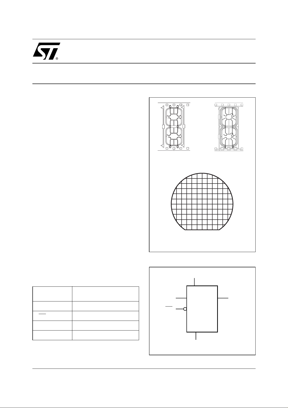
The M14C32 is available in wafer form (either
sawn or unsawn) and in micromodule form (on
film). The M14C64 is available in micro-module
2
2
Micromodule (D20)
2
2
Wafer
Figure 1. Logic Diagram
Micromodule (D22)
Table 1. Signal Names
SDA Serial Data/Address Input/
Output
SCL Serial Clock
WC
V
CC
GND Ground
Write Control
Supply Voltage
SCL
V
CC
GND
SDA
M14xxxWC
AI02217
1/14October 1999
Page 2
M14C64, M14C32
Figure 2. D20 Contact Connections
V
CC
GND
WC
SCL
SDA
AI02168
form only. For availability of the M14C64 in wafer
form, please contact your ST sales office.
Each memory is compatible with the I
2
C extended
memory standard. This is a two wire serial interface that uses a bi-directional data bus and serial
clock. The memory carries a built-in 7-bit unique
Device Type Identifier code (1010000) in accordance with the I
can be attached to each I
The memory behaves as a slave device in the I
2
C bus definition. Only one memory
2
C bus.
2
protocol, with all memory operations synchronized
by the serial clock. Read and write o perations are
initiated by a START condition, gene rated by the
bus master. The STA RT condition is followed by
the Device Select Code which is compos ed of a
stream of 7 bits (1010000), plus one read/write bit
(R/W
) and is terminated by an acknowledge bit.
When writing data to the memory, the mem ory inserts an acknowledge bit during the 9
th
bit time,
Figure 3. D22 Contact Connections
V
CC
WC
SCL
following the bus master’s 8-bit transmission.
When data is read by the bus master, the bus
master acknowledges the receipt of the data byte
in the same way. Data transfers are terminated by
a STOP condition after an Ack for WRITE, and after a NoACK for READ.
Power On Reset: V
Lock-Out Write Protect
CC
In order to prevent data corruption and inadvertent
write operations during power up, a Power On Re-
C
set (POR) circuit is included. The internal reset is
held active until the V
voltage has reached the
CC
POR threshold value, and all operations are disabled – the device will not respond to any command. In the same way, when V
drops from the
CC
operating voltage, below the POR threshold value,
all operations are disabled and the device will not
respond to any com ma nd. A s table a nd v alid V
must be applied before applying any logic signal.
GND
SDA
AI02204
CC
Table 2. Absolute Maximum Ratings
Symbol Parameter Value Unit
T
A
T
STG
V
IO
V
CC
V
ESD
Note: 1. Exc ept for the rating “Operating Temperature Range”, stresses above those l i sted in the Table “Absolute Maximum Ratings” may
2/14
cause permanent damage to the device. These are stress ratings only, and operation of the device at these or any other conditions
above those indica te d i n the Operating secti ons of this specification is not im plied. Exposure to Absolute Ma xim um Rating conditions for extended periods may affect device reliability. Refer also to the ST SURE Program and other relevant quality documents.
2. MIL -STD-883C, 3015.7 (100 pF, 1500 Ω )
3. EIA J I C-121 (Condi tion C) (200 pF, 0 Ω)
Ambient Operating Temperature 0 to 70 °C
Storage Temperature
Input or Output range -0.6 to 6.5 V
Supply Voltage -0.3 to 6.5 V
Electrostatic Discharge Voltage (Human Body model)
Electrostatic Discharge Voltage (Machine model)
1
Wafer form
Module form
2
3
-65 to 150
-40 to 120
4000 V
400 V
°C
Page 3
M14C64, M14C32
SIGNAL DESCRIPTION
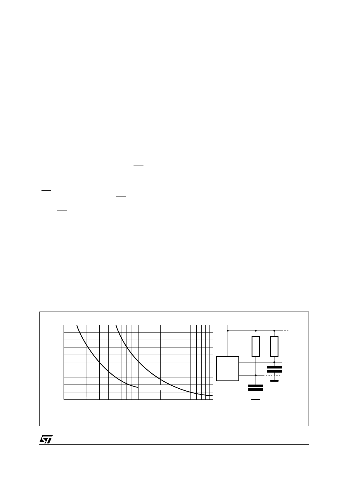
Serial Clock (SCL)
The SCL input pin is used to sync hronize all data
in and out of the memory. A pull up resistor can be
connected from the SCL line to V
. (Figure 4 in-
CC
dicates how the value of the pull-up resistor can be
calculated).
Serial Data (SDA)
The SDA pin is bi-directional, and is used to transfer data in or out of the memory. It is an open drain
output that may be wire-OR’ed with other open
drain or open collector signals on the bus. A pull
up resistor must be connected from the SDA bus
to V
. (Figure 4 indicates how the value of the
CC
pull-up resistor can be calculated).
Write Control (WC
The hardware Write Control contact (WC
)
) is useful
for protecting the entire contents of the memory
from inadvertent erase/write. The Write Control
signal is used to enable (WC
(WC
=VIH) write instructions to the entire memory
area. When unconnected, the WC
ly read as V
When WC
and write operations are allowed.
IL
=1, Device Select and Address bytes
=VIL) or disable
input is internal-
are acknowledged, Data bytes are not acknowledged.
Please see the Application Note
AN404
for a more
detailed description of the Write Control feature.
DEVICE OPERATION
2
The memory device supports the XI
2
I
C) protocol, as summarized in Figure 5. Any de-
C (Extended
vice that sends data on to the bus is defined to be
a transmitter, and any dev ice that reads the dat a
to be a receiver. The device that controls the data
transfer is known as the master, and the other as
the slave. A data transfer can o nly be initiated by
the master, which will also provide the serial clock
for synchronization. The memory device is always
a slave device in all communication.
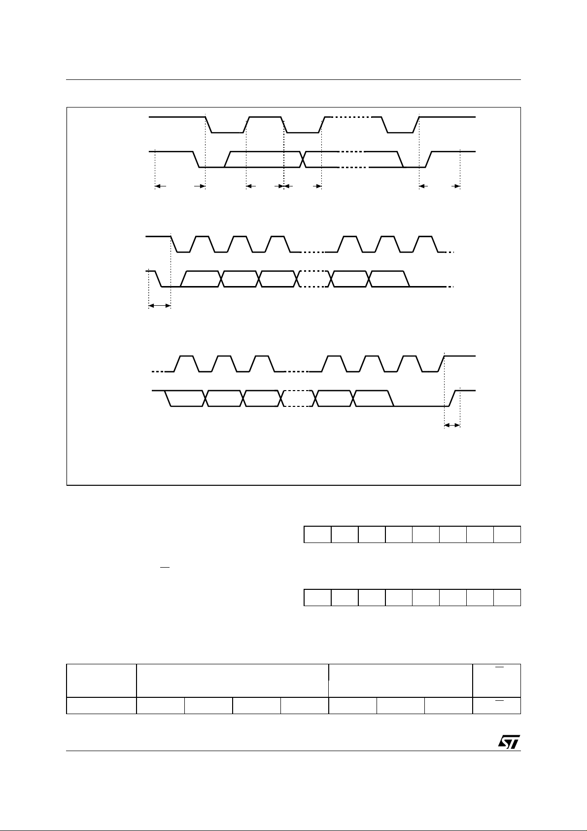
Start Condition
START is identified by a high t o low transition of
the SDA line while the clock, SCL, is stable i n the
high state. A START condition must precede any
data transfer comman d. Th e m em ory devi ce continuously monitors (except during a program ming
cycle) the SDA and SCL lines for a START condition, and will not respond unless one is given.
Stop Condition
STOP is identified by a low to high transition of the
SDA line wh ile th e clock S CL is sta ble in the h igh
state. A STO P condition terminates c ommunication between the memory device and the bus master. A STOP condition at the end of a Read
command, after (and only after) a NoACK , forces
the memory device into its standby state. A STOP
condition at the end of a Write command triggers
the internal EEPRO M writ e cycle.
Acknowledge Bit (ACK)
An acknowledge signal is used to indicate a successful data transfer. The bus transmitter, either
master or slave, will release the SDA bus after
sending 8 bits of data. During t he 9
th
clock pulse
period the receiver pulls the SDA bus low to acknowledge the receipt of the 8 data bits.
Data Input
During data input, the memory device samples the
SDA bus signal on the rising edge of the clock,
SCL. For correct device operation, the SDA signal
must be stable during the clock low-to-high transition, and the data must change
only
when the SCL
line is low.
Figure 4. Maximum R
20
16
12
8
Maximum RP value (kΩ)
4
0
10 1000
Value versus Bus Capacitance (C
L
fc = 100kHz
fc = 400kHz
100
C
(pF)
BUS
) for an I2C Bus
BUS
V
MASTER
CC
SDA
SCL
R
R
C
BUS
L
C
BUS
AI01665
3/14
L
Page 4
M14C64, M14C32
2
Figure 5. I
C Bus Protocol
SCL
SDA
SCL
SDA
SCL
SDA
START
CONDITION
START
CONDITION
SDA
INPUT
1 23 789
MSB
1 23 789
MSB ACK
SDA
CHANGE
CONDITION
ACK
STOP
STOP
CONDITION
AI00792
Memory Addressing
To start communication betwee n the bus master
and the slave memory, the master must initiate a
START condition. Following this, the master sends
8 bits to the SDA bus line (with the most significant
bit first). These bits represent the Device Select
Code (7 bits) and a RW
bit.
The seven most s ignificant bits of the Device Select Code are the Device Type Identifier, according
to the I
Table 5. Device Select Code
Note: 1. The most significant bit, b7, is sent first.
4/14
2
C bus definition. For the mem ory device,
1
Device Code Chip Enable RW
b7 b6 b5 b4 b3 b2 b1 b0
Device Select 1010000RW
Table 3. Most Significant Byte
b15 b14 b13 b12 b11 b10 b9 b8
Note: 1. b15 to b13 are Don’t Care on the M14C6 4 series.
b15 to b12 are Don’t Care on the M 14C32 serie s.
Table 4. Least Significant Byte
b7 b6 b5 b4 b3 b2 b1 b0
Page 5
M14C64, M14C32
the seven bits are fixed at 1010000b (A0h), as
shown in Table 5.
th
The 8
bit is the read or write bit (RW). This bit is
set to ‘1’ for read and ‘0’ for write operations. If a
match occurs on the Device Select Code, the corresponding memory gives an acknowledgment on
the SDA bus during the 9
th
bit time. If the memory
does not match the Device Select code, it will deselect itself from the bus, and go into stand-by
mode.
Each data byte in the m emory has a 16-bit (two
byte wide) address. The Most Significant Byte (Table 3) is sent first, f ollowed by the Least significant
Byte (Table 4). Bits b15 to b0 form t he addre ss of
the byte in memory. Bits b15 to b13 are treated as
a Don’t Care bit on the M14C64 memory. Bits b15
to b12 are treated as Don’t Care bits on the
M14C32 me m o r y .
Write Operations
Following a START con dition the ma ster sends a
Device Select code with the RW
bit set to ’0’, as
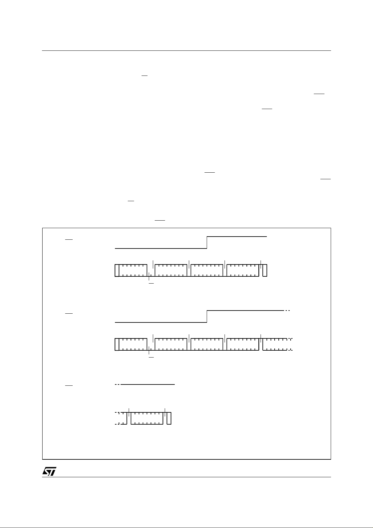
Figure 6. Wri te Mo de S e qu e nces with WC=1
WC
shown in Table 6. The memory acknowledges it
and waits for two bytes of address, which provides
access to the memory area. After receipt of each
byte address, the memory again responds with an
acknowledge and waits for t he data byte. Writing
in the memory may be inhibited if input pin WC
is
taken high.
Any write command with WC
=1 (during a period of
time from the START condition until the end of the
two bytes address) will not modify the memory
content and will NOT be acknowledged on data
bytes, as shown in Figure 6.
Byte Write
In the Byte Write mode, after the Device Select
code and the address, the master sends one data
byte. If the addressed location is write protected by
the W C
pin, the memory replies with a NoACK,
and the location is not modified. If, instead, the WC
pin has been held at 0, as shown in F igure 7, the
memory replies with an ACK. The master terminates the transfer by generating a STOP condition.
ACK ACK ACK NO ACK
BYTE WRITE DEV SEL BYTE ADDR BYTE ADDR DATA IN
R/W
START
WC
ACK ACK ACK NO ACK
PAGE WRITE DEV SEL BYTE ADDR BYTE ADDR DATA IN 1
R/W
START
WC (cont'd)
NO ACK NO ACK
PAGE WRITE
(cont'd)
DATA IN N
STOP
DATA IN 2
STOP
AI01120B
5/14
Page 6

M14C64, M14C32
Table 6. Operating Modes
Mode RW bit
Current Address Read ‘1’ X 1 START, Device Select, RW
‘0’ X START, Device Select, RW
Random Address Read
‘1’ X 1 reSTART, Device Select, RW
Sequential Read ‘1’ X ≥ 1 Similar to Current or Random Mode
Byte Write ‘0’
Page Write ‘0’
Note: 1. X = V
IH
or V
.
IL
Figure 7. Wri te Mo de S e qu e nces with WC=0
WC
WC
V
V
1
Bytes Initial Sequence
= ‘1’
= ‘0’, Address
= ‘1’
IL
IL
1 START, Device Select, RW = ‘0’
≤ 32 START, Device Select, RW = ‘0’
ACK
BYTE WRITE DEV SEL BYTE ADDR BYTE ADDR DATA IN
R/W
START
WC
ACK ACK ACK ACK
PAGE WRITE DEV SEL BYTE ADDR BYTE ADDR DATA IN 1
R/W
START
WC (cont'd)
ACKACK
PAGE WRITE
(cont'd)
DATA IN N
ACK ACK ACK
STOP
DATA IN 2
STOP
Page Write
The Page Write mode allows u p to 32 by tes to be
written in a single write cycle, provided that they
are all located in the same ’row’ in the memory:
that is the most significant memory add ress bits
(b13-b5 for the M14C64 and b12-b5 for the
6/14
AI01106B
M14C32) are the same. The m aster sends from
one up to 32 bytes of data, each of which is acknowledged by the memory if the WC
the WC
pin is high, each data byte is followed by a
pin is low. If
NoACK and the location is not modified. After each
byte is transferred, the internal byte address counter (the five least significant bits only) is increment-
Page 7

Figure 8. Wri te Cy cle Pol l in g Fl owchart using AC K
WRITE Cycle
in Progress
START Condition
DEVICE SELECT
with RW = 0
ACK
NO
Returned
M14C64, M14C32
First byte of instruction
with RW = 0 already
decoded by M14xxx
ReSTART
STOP
YES
Next
Operation is
Addressing the
Memory
WRITE Operation
ed. The transfer is terminated by the master
generating a STOP condition. Care must be taken
to avoid address counter ’roll-over’ which could result in data being overwritten. Note that, for any
byte or page write mode, the generation by the
master of the STOP condition starts the internal
memory program cycle. This STOP condition triggers an internal memory program cycle only if the
STOP condition is internally decoded immediately
after the ACK bit; any STOP condition decoded
out of this "10
th
bit" time slot will not trigger the internal programming cycle. All inputs are disabled
until the completion of this cycle and the Memory
will not respond to any request.
Minimizing System Delays by Polling On ACK
During the internal write cycle, the memory disconnects itself from the bus, and copies the data from
its internal latches to the memory cells. The maximum write time (t
) is indicated in Table 7, but the
w
YESNO
Send
Byte Address
Proceed
Proceed
Random Address
READ Operation
AI02165
typical time is shorter. To make use of this, an ACK
polling sequence can be used by the master.
The sequence, as shown in Figure 8, is as follows:
– Initial condition: a Write is in progress.
– Step 1: the m aster issues a START condition
followed by a device select byte (first byte of the
new instruction).
– Step 2: if the memory is busy with the internal
write cycle, no ACK will be returned and the
master goes back to Step 1. If the memory has
terminated the internal write cycle, it responds
with an ACK, indicating that the memory is
ready to receive the second part of the next instruction (the first byte of this instruction having
been sent during Step 1).
Read Operations
Read operations are inde pendent of the state of
the WC
pin. On delivery, the memory content is set
at all “1’s” (FFh).
7/14
Page 8

M14C64, M14C32
Figure 9. Read Mode Sequences
CURRENT
ADDRESS
READ
RANDOM
ADDRESS
READ
SEQUENTIAL
CURRENT
READ
SEQUENTIAL
RANDOM
READ
ACK
DEV SEL DATA OUT
R/W
START
ACK
DEV SEL * BYTE ADDR BYTE ADDR
R/W
START
ACK ACK ACK NO ACK
DEV SEL DATA OUT 1
R/W
START
ACK ACK ACK
DEV SEL * BYTE ADDR BYTE ADDR
NO ACK
STOP
ACK ACK ACK
DEV SEL * DATA OUT
R/W
START
DATA OUT N
STOP
ACK ACK
DEV SEL * DATA OUT 1
NO ACK
STOP
R/W
START
ACK NO ACK
DATA OUT N
STOP
Note: 1. The seven most signi fi cant bits of the D evice Select by tes of a Random Read (in the 1st and 4th bytes) must be identi cal.
Current Address Read
The memory has an internal address counter.
Each time a byte is read, this counter is incremented. For the Current Address Read mode, following
a START condition, the master sends a device select with the RW
bit set to ‘1’. The memory acknowledges this, an d outpu ts the byt e address ed
by the internal address counter. The counter is
not
then incremented. The master must
acknowledge the byte output, and terminates the transfer
with a STOP condition, as shown in Figure 9.
Random Address Read
A dummy write is performed to load the address
into the address counter, as shown in Figure 9.
This is followed by another START condition from
the master and the device selec t is repeated with
the R W
this, and outputs the byte addressed. The master
must
nates the transfer with a STOP condition.
Sequenti a l Rea d
This mode can be initiated with either a Current
START
bit set to ‘1’. The m emory acknowledges
not
acknowledge the byte out put, and termi-
R/W
AI01105C
Address Read or a Random A ddress Read. How-
does
ever, in this case the master
acknowledge
8/14
Page 9

M14C64, M14C32
the data byte output, and the memory continues to
output the next byte in sequence. To terminate the
stream of bytes, the master must
the last byte ou tput, and
must
not
acknowledge
generate a STOP
condition. The output data comes from consecutive addresses, with the internal address c ounter
automatically incremen ted af t er ea ch byt e out put.
After the last memory address, the address
counter will ‘roll -ove r’ and the me mor y will c ontin -
ue to output data from the start of the memory
block.
Acknowledge in Read Mode
In all read modes the memory waits for an acknowledgment during the 9
th
bit time. If the master
does not pull the SDA line l ow during this time, the
memory terminates the data transfer and switches
to its standby state.
9/14
Page 10

M14C64, M14C32
Table 7. AC Characteristics
(T
= 0 to 70 °C; VCC = 2.5 V to 5.5 V )
A
Symbol Alt. Parameter
2
t
CH1CH2
2
t
CL1CL2
2
t
DH1DH2
2
t
DL1DL2
1
t
CHDX
t
CHCL
t
DLCL
t
CLDX
t
CLCH
t
DXCX
t
CHDH
t
DHDL
t
CLQV
t
CLQX
f
C
t
W
Note: 1. For a r eS T ART conditio n, or following a w ri te cycle.
2. Samp l ed only, not 100 % tested
t
R
t
F
t
R
t
F
t
SU:STA
t
HIGH
t
HD:STA
t
HD:DAT
t
LOW
t
SU:DAT
t
SU:STO
t
BUF
t
AA
t
DH
f
SCL
t
WR
Clock Rise Time 300 1000 ns
Clock Fall Time 300 300 ns
SDA Rise Time 20 300 20 1000 ns
SDA Fall Time 20 300 20 300 ns
Clock High to Input Transition 600 4700 ns
Clock Pulse Width High 600 4000 ns
Input Low to Clock Low (START) 600 4000 ns
Clock Low to Input Transition 0 0 µs
Clock Pulse Width Low 1.3 4.7 µs
Input Transition to Clock Transition 100 250 ns
Clock High to Input High (STOP) 600 4000 ns
Input High to Input Low (Bus Free) 1.3 4.7 µs
Clock Low to Data Out Valid 1000 3500 ns
Data Out Hold Time After Clock Low 200 200 ns
Clock Frequency 400 100 kHz
Write Time 10 10 ms
2
Fast I
C
400 kHz
I2C
100 kHz
Min Max Min Max
Unit
Table 8. DC Characteristics
= 0 to 70 °C; VCC = 2.5 V to 5.5 V )
(T
A
Symbol Parameter Test Condition Min. Max. Unit
10/14
I
LI
I
LO
I
CC
I
CC1
V
IL
V
IH
V
IL
V
IH
V
OL
Input Leakage Current
Output Leakage Current
V
=5V, fc=400kHz (rise/fall time < 30ns)
CC
Supply Current
V
=2.5V, fc=400kHz (rise/fall time < 30ns)
CC
Supply Current
(Stand-by)
Input Low Voltage (SCL, SDA) - 0.3 0.3 V
Input High Voltage (SCL, SDA) 0.7 V
Input Low Voltage (WC) - 0.3 0.5 V
Input High Voltage (WC)
Output Low
Voltage
0V ≤ V
0V ≤ V
OUT
V
= VSS or V
IN
V
= VSS or V
IN
I
= 3 mA, VCC = 5 V
OL
I
= 2.1 mA, VCC = 2.5 V 0.4 V
OL
≤ V
≤ V
IN
SDA in Hi-Z
CC,
, V
CC
, V
CC
CC
CC
= 5 V
CC
= 2.5 V 2 µA
CCVCC
V
- 0.5 VCC + 1
CC
± 2 µA
± 2 µA
2mA
1mA
20 µA
CC
+ 1 V
0.4 V
V
V
Page 11

Figure 10. AC Waveforms
M14C64, M14C32
SCL
SDA IN
SCL
SDA OUT
SCL
tCHCL
tDLCL
tCHDX
START
CONDITION
tCLQV tCLQX
tCLDX
SDA
INPUT
DATA VALID
DATA OUTPUT
SDA
CHANGE
tW
tCLCH
tDXCX
tCHDH
tDHDL
STOP &
BUS FREE
SDA IN
tCHDH
STOP
CONDITION
Table 9. AC Measurement Conditions
Input Rise and Fall Times ≤ 50 ns
0.2V
0.3V
to 0.8V
CC
to 0.7V
CC
Input Pulse Voltages
Input and Output Timing
Reference Voltages
WRITE CYCLE
CC
CC
Figure 11. AC Testing Input Output Waveforms
0.8V
CC
0.2V
CC
tCHDX
START
CONDITION
AI00795B
Table 10. Input Parameters1 (TA = 25 °C, f = 400 kHz)
Symbol Parameter Test Condition Min. Max. Unit
C
IN
C
IN
t
NS
Note: 1. Sampled only, not 100% tested.
Input Capacitance (SDA) 8 pF
Input Capacitance (other pins) 6 pF
Low Pass Filter Input Time
Constant (SCL & SDA Inputs)
100 400 ns
0.7V
0.3V
AI00825
CC
CC
11/14
Page 12

M14C64, M14C32
Table 11. Ordering Information Scheme
Example 1: M14C64 - W D22
Memory Capacity Delivery Form
64 64 Kbit D22
32 32 Kbit D20
Operating Voltage
W 2.5 V to 5.5 V
Example 2: M14C32 - W W2
Module on Super 35 mm
film (M14C64 only)
Module on Super 35 mm
film (M14C32 only)
Memory Capacity Delivery Form
32 32 Kbit W2
Operating Voltage
W 2.5 V to 5.5 V S2x
where “x” indicates the sawing orientation, as follows (and as shown in Figure 12)
ORDERING INFORMATION
Devices are shipped from the factory with the
memory content set at all ‘1’s (FFh).
The notation used for the device number is as
shown in Table 11. For a list of available options
(speed, package, etc.) or for further information on
any aspect of this device, please contact the ST
Sales Office nearest to you.
Sawn wafers are scribed an d m ount ed in a frame
on adhesive tape. The orientation is defined by the
position of the GND pad on the die, viewed with
es of the frame (as shown in Figure 12). The orientation of the die with respect t o the plastic frame
notches is specified by the Customer.
One further concern, when specify ing devices to
be delivered in this form, is that wafers mounted
on adhesive tape must be used within a limited period from the mounting date:
– two months, if waf ers are stored a t 25°C, 55%
relative h umidity
– six months, if wafers are stored at 4°C, 55% rel-
ative humidity
Unsawn wafer (275 µm ±
25 µm thickness)
Unsawn wafer (180 µm ±
W4
15 µm thickness)
Sawn wafer (275 µm ± 25
µm thickness)
Sawn wafer (180 µm ± 15
S4x
µm thickness)
1 GND at top right
2 GND at bottom right
3 GND at bottom left
4 GND at top left
active area of product visible, relative to the notch-
12/14
Page 13

Figure 12. Sawing Orientation
M14C64, M14C32
VIEW: WAFER FRONT SIDE
GND
1ORIENTATION
GND
GND GND
234
AI02171
13/14
Page 14

M14C64, M14C32
Information furnished is believed to be accurate and reliable. However, STMicroelectronics assumes no responsibility for the consequences
of use of such information nor for any infringement of patents or other rights of third parties which may result from its use. No license is granted
by implic ation or otherwise under any patent or patent right s of STMicroelectronics . S pecifications mentioned i n this public ation ar e subject
to change without notice. This publication supersedes and replaces all information previously supplied. STMicroelectronics products are not
authorized for use as criti cal components i n l i f e support device s or systems without express written approval of STMicroelec tr o nics.
© 1999 STMicroelectronics - All Rights Reserved
The ST logo is a registered trademark of ST M i croelectronics.
All other na m es are the proper ty of their respecti ve owners.
STMicroelec tron ics GROUP OF COMPANIES
Australia - Brazil - China - France - Germany - Italy - Japan - Korea - Malaysia - Malta - Mexico - Morocco - The Netherlands - Singapore -
Spain - Sweden - Switzerland - Taiwan - Thai land - United Kingdom - U.S. A.
http://www.s t. com
14/14
 Loading...