

Page 1
M14256
M14128
Memory Card IC
256/128 Kbit Serial I²C Bus EEPROM
PRELIMINARY DATA
■ Compat ible with I
■ Two Wire I
2
C Extended Addressing
2
C Serial Interface
Supports 400 kHz Protocol
■ Single Supply Voltage (2.5 V to 5.5 V)
■ Hardware Write Control
■ BYTE and PAGE WRITE (up to 64 Bytes)
■ BYTE, RANDOM and SEQUENTIAL READ
Modes
■ Self-Tim e d P ro g r amming Cycle
■ Automatic Address Incrementing
■ Enhanced ESD/Latch-Up Behaviour
■ 100,000 Erase/Write Cycles (minimum)
■ 40 Year Data Retention (minimum)
■ 5 ms Programming Time (typical)
DESCRIPTION
Each device is an electrically erasable program mable memory (EEPROM) fabricated with STMi-
croelectronics’s High Endurance, Double
Polysilicon, CMOS technology. This guarantees
an endurance typically well above 100,000 Erase/
Write cycles, with a data retention of 40 years. The
memory operates with a powe r supply as low as
2.5 V.
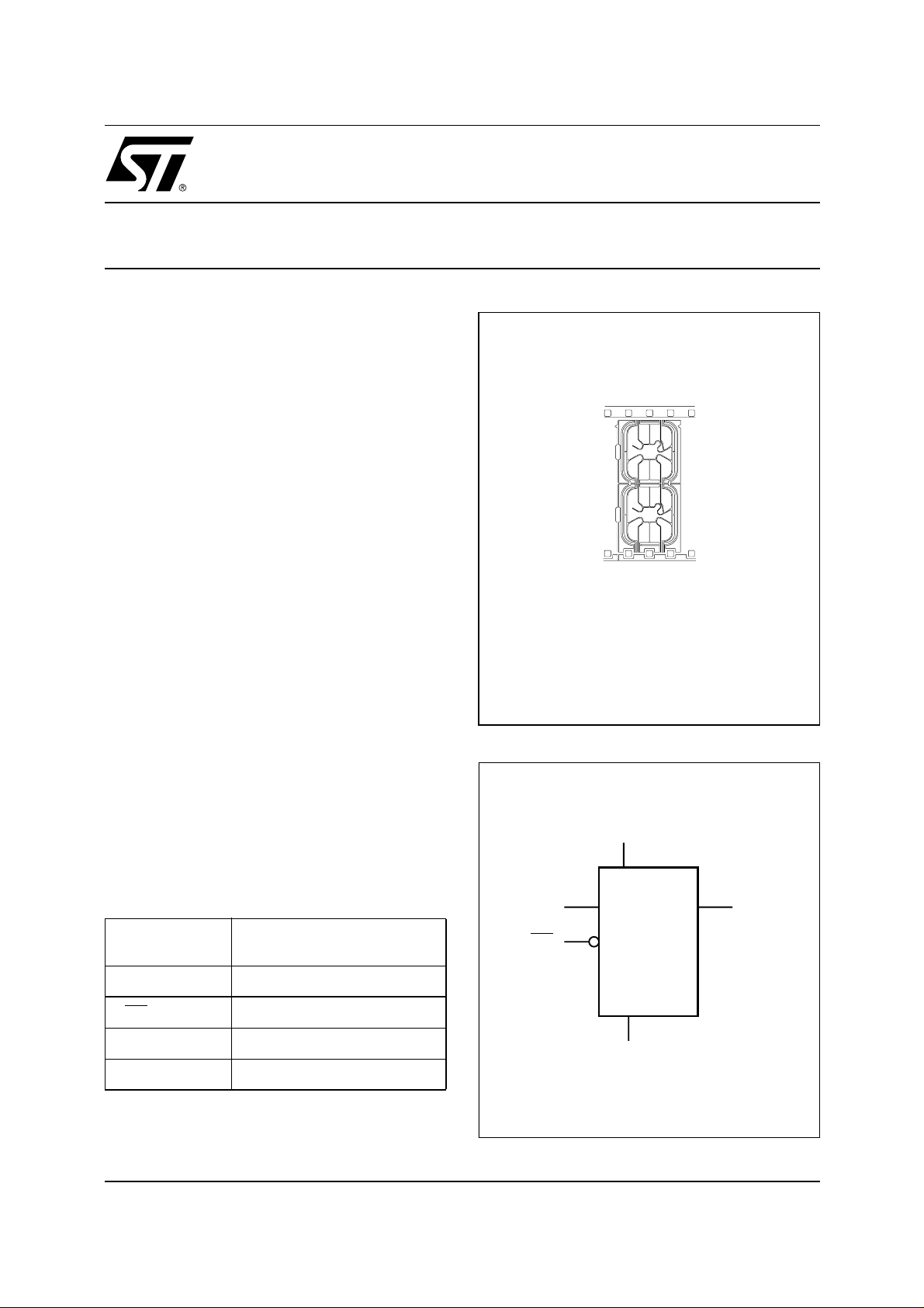
The M14256 and M 14128 are avail able in micro-
module form only. For availability of the M14256 or
Micromodule (D22)
Figure 1. Logic Diag ram
V
CC
Table 1. Signal Names
SDA Serial Data/Address Input/
Output
SCL Serial Clock
WC
V
CC
GND Ground
October 1999
This is preliminary information on a new product now in development or undergoing evaluation. Details are subject to change without notice.
Write Control
Supply Voltage
SCL
M14xxxWC
GND
SDA
AI02217
1/12
Page 2
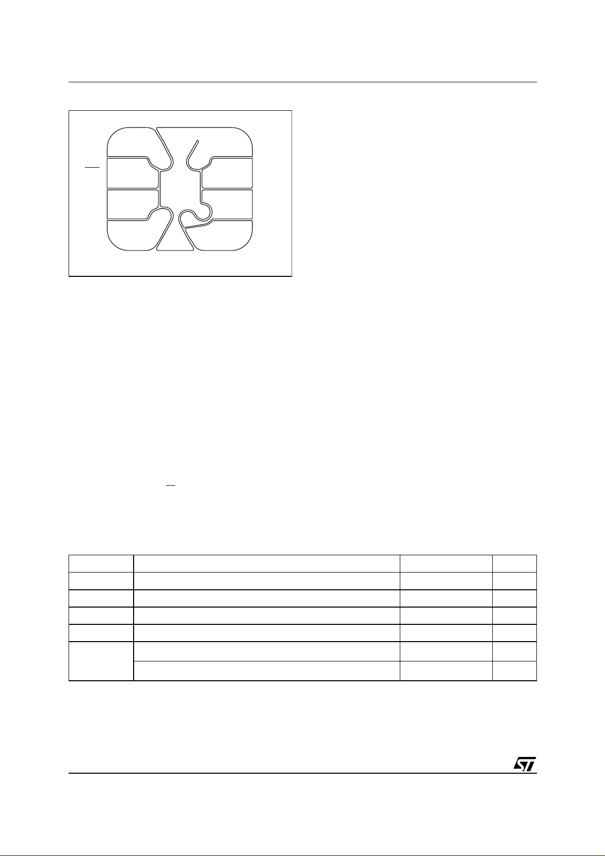
M14256, M14128
Figure 2. D22 Contact Connections
V
CC
WC
SCL
GND
SDA
AI02204
M14128 in wafer form, please contact your ST
sales office.
Each memory device is compatible with the I
2
extended memory standard. This is a two wire serial interface that uses a bi-directional data bus
and serial clock. The memory device carries a
built-in 7-bit unique Device Type Identifier code
(1010000) in accordance with the I
tion. Only one memory de vice can be attached to
2
each I
The memory device behaves as a slave dev ice in
the I
C bus.
2
C protocol, with all memory operations syn-
2
C bus d efini-
chronized by the serial clock. Read and write operations are initiated by a START condition,
generated by the bus master. T he START condition is followed by the Device Select Code which is
composed of a stream of 7 bits (1010000), plus
one read/write bit (R/W
) and is terminated by an
acknowledge bit.
When writing data to the m emory, the memory device inserts an acknowledge bit during the 9
time, following the bus master’s 8-bit transmission.
When data is read by the bus master, the bus
master acknowledges the receipt of the data byte
in the same way. Data transfers are terminated by
a STOP condition after an Ack for WRITE, and after a NoACK for READ.
Power On Reset: V
Lock-Out Write Protect
CC
In order to prevent data corruption and inadvertent
write operations during power up, a Power On Reset (POR) circuit is included. The internal reset is
held active until the V
voltage has reached the
CC
POR threshold value, and all operations are disabled – the device will not respond to any command. In the same way, when V
drops from the
CC
operating voltage, below the POR threshold value,
all operations are disabled and the device will not
respond to any com ma nd. A s table a nd v alid V
must be applied before applying any logic signal.
C
SIGNAL DESCRIPTION
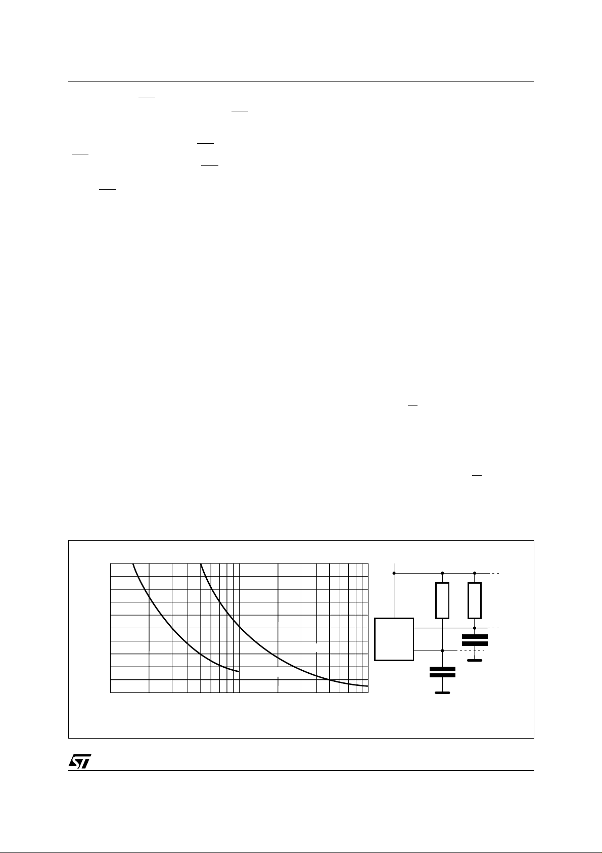
Serial Clock (SCL)
The SCL input pin is used to synchronize a ll data
in and out of the memory. A pull up resistor can be
connected from the SCL line to V
CC
dicates how the value of the pull-up resistor can be
calculated).
Serial Data (SDA)
The SDA pin is bi-directional, and is used to transfer data in or out of the memory. It is an open drain
output that may be wire-OR’ed with other open
drain or open collector signals on the bus. A pull
up resistor must be connected from the SDA bus
to V
. (Figure 3 indicates how the value of the
CC
pull-up resistor can be calculated).
th
bit
CC
. (Figure 3 in-
Table 2. Absolute Maximum Ratings
Symbol Parameter Value Unit
T
A
T
STG
V
IO
V
CC
V
ESD
Note: 1. Exc ept for the rating “Operating Temperature Ra nge”, stres ses above those listed in the Table “Absolute Maximum Ratings” may
2/12
cause permanent damage to the device. These are stress ratings only, and operation of the device at these or any other conditions
above those indi cated in t he Operating sect i ons of thi s specifi cation i s not impl i ed. Exposure to Absolute M aximum Rating c onditions for extended periods may affect device reliability. Refer also to the ST SURE Program and other relevant quality documents.
2. MIL -STD-883C, 3015.7 (1 00 pF, 1500 Ω)
3. EIA J I C-121 (Condition C) (200 pF, 0 Ω)
Ambient Operating Temperature 0 to 70 °C
Storage Temperature -40 to 120 °C
Input or Output range -0.6 to 6.5 V
Supply Voltage -0.3 to 6.5 V
Electrostatic Discharge Voltage (Human Body model)
Electrostatic Discharge Voltage (Machine model)
1
2
3
4000 V
400 V
Page 3
M14256, M14128
Write Control (WC)
The hardware Write Control contact (WC
) is useful
for protecting the entire contents of the memory
from inadvertent erase/write. The Write Control
signal is used to enable (WC
(WC
=VIH) write instructions to the entire memory
area. When unconnected, the WC
ly read as V
When WC
and write operations are allowed.
IL
=1, Device Select and Address bytes
=VIL) or disable
input is internal-
are acknowledged, Data bytes are not acknowledged.
Please see the Application Note
AN404
for a more
detailed description of the Write Control feature.
DEVICE OPERATION
2
The memory device supports the XI
2
C) protocol, as summarized in Figure 4. Any de-
I
C (Extended
vice that sends data on to the bus is defined to be
a transmitter, and any dev ice that reads the dat a
to be a receiver. The device that controls the data
transfer is known as the master, and the other as
the slave. A data transfer can o nly be initiated by
the master, which will also provide the serial clock
for synchronization. The memory device is always
a slave device in all communication.
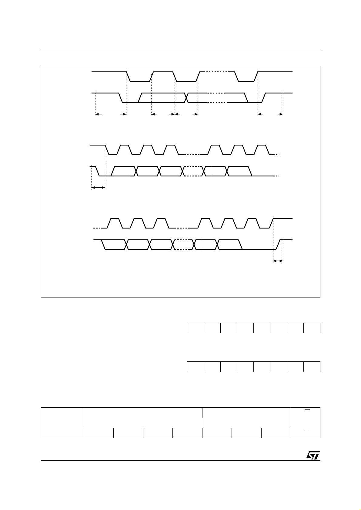
Start Condition
START is identified by a high t o low transition of
the SDA line while the clock, SCL, is s table i n t he
high state. A START condition must precede any
data transfer comman d. Th e m em ory devi ce continuously monitors (except during a program ming
cycle) the SDA and SCL lines for a START condition, and will not respond unless one is given.
Stop Condition
STOP is identified by a low to high transition of the
SDA line while the clock, SCL, is stable in the high
state. A STO P condition terminates c ommunication between the memory device and the bus master. A STOP condition at the end of a Read
command, after (and only after) a NoACK , forces
the memory device into its standby state. A STOP
condition at the end of a Write command triggers
the internal EEPROM write cycle.
Acknowledge Bit (ACK)
An acknowledge signal is used to indicate a successful data transfer. The bus transmitter, either
master or slave, will release the SDA bus after
sending 8 bits of data. During t he 9
th
clock pulse
period the receiver pulls the SDA bus low to acknowledge the receipt of the 8 data bits.
Data Input
During data input, the memory device samples the
SDA bus signal on the rising edge of the clock,
SCL. For correct device operation, the SDA signal
must be stable during the clock low-to-high transi-
only
tion, and the data must change
when the SCL
line is low.
Memory Addressing
To start communication betwee n the bus master
and the slave memory, the master must initiate a
START condition. Following this, the master sends
8 bits to the SDA bus line (with the most significant
bit first). These bits represent the Device Select
Code (7 bits) and a RW
bit.
The seven most s ignificant bits of the Device Select Code are the Device Type Identifier, according
to the I
2
C bus definition. For the mem ory device,
the seven bits are fixed at 1010000b (A0h), as
shown in Table 5.
th
The 8
bit is the read or write bit (RW). This bit is
set to ‘1’ for read and ‘0’ for write operations. If a
match occurs on the Device Select Code, the cor-
Figure 3. Maximum R
20
16
12
8
Maximum RP value (kΩ)
4
0
10 1000
Value versus Bus Capacitance (C
L
fc = 100kHz
fc = 400kHz
100
C
(pF)
BUS
) for an I2C Bus
BUS
V
MASTER
CC
SDA
SCL
R
R
C
BUS
L
C
BUS
AI01665
3/12
L
Page 4
M14256, M14128
2
Figure 4. I
C Bus Protocol
SCL
SDA
SCL
SDA
SCL
SDA
START
CONDITION
START
CONDITION
SDA
INPUT
1 23 789
MSB
1 23 789
MSB ACK
SDA
CHANGE
CONDITION
ACK
STOP
STOP
CONDITION
AI00792
responding memory gives an acknowledgment on
the SDA bus during the 9
does not match the Device Select code, it will deselect itself from the bus, and go into stand-by
mode.
Each data byte in the m emory has a 16-bit (two
th
bit time. If the memory
Table 3. Most Significant Byte
b15 b14 b13 b12 b11 b10 b9 b8
Note: 1. b15 is Don’t Care on the M14256 series.
b15 and b14 ar e Don’t Care on t he M 14128 seri es.
byte wide) address. The Most Significant Byte (Table 3) is sent first, f ollowed by the Least significant
Byte (Table 4). Bits b15 to b0 form t he addre ss of
the byte in memory. Bit b15 is t reated as a Don’t
Table 4. Least Significant Byte
b7 b6 b5 b4 b3 b2 b1 b0
Care bit on the M14256 memory. Bits b15 and b14
are treated as Don’t Care bits on the M14128
memory.
Table 5. Device Select Code
b7 b6 b5 b4 b3 b2 b1 b0
Device Select 1010000RW
Note: 1. The most significant bit, b7, is sent firs t.
4/12
1
Device Code Chip Enable RW
Page 5

M14256, M14128
Write Operations
Following a START con dition the ma ster sends a
Device Select code with the RW
bit set to ’0’, as
shown in Table 6. The memory acknowledges it
and waits for two bytes of address, which provides
access to the memory area. After receipt of each
byte address, the memory again responds with an
acknowledge and waits for t he data byte. Writing
in the memory may be inhibited if the input pin WC
is taken high.
Any write command with WC
=1 (during a period of
time from the START condition until the end of the
two bytes address) will not modify the memory
content and will NOT be acknowledged on data
bytes, as shown in Figure 5.
Byte Write
In the Byte Write mode, after the Device Select
code and the address, the master sends one data
byte. If the addressed location is write protected by
the W C
pin, the memory replies with a NoACK,
and the location is not modified. If, instead, the WC
Figure 5. Wri te Mo de S e qu e nces with WC =1
WC
pin has been held at 0, as shown in F igure 6, the
memory replies with an ACK. The master terminates the transfer by generating a STOP condition.
Page Write
The Page Write mode allows u p to 64 by tes to be
written in a single write cycle, provided that they
are all located in the same ’row’ in the memory:
that is the most significant memory add ress bits
(b14-b6 for the M14256 and b13-b6 for the
M14128) are the same. The master sends from
one up to 64 bytes of data, each of which is acknowledged by the memory if the WC
the WC
pin is high, each data byte is followed by a
pin is low. If
NoACK and the location is not modified. After each
byte is transferred, the internal byte address counter (the six least significant bits only) is incremented. The transfer is terminated by the master
generating a STOP condition. Care must be taken
to avoid address counter ’roll-over’ which could result in data being overwritten. Note that, for any
ACK ACK ACK NO ACK
BYTE WRITE DEV SEL BYTE ADDR BYTE ADDR DATA IN
R/W
START
WC
ACK ACK ACK NO ACK
PAGE WRITE DEV SEL BYTE ADDR BYTE ADDR DATA IN 1
R/W
START
WC (cont'd)
NO ACK NO ACK
PAGE WRITE
(cont'd)
DATA IN N
STOP
DATA IN 2
STOP
AI01120B
5/12
Page 6

M14256, M14128
Table 6. Operating Modes
Mode RW bit
Current Address Read ‘1’ X 1 START, Device Select, RW
‘0’ X START, Device Select, RW
Random Address Read
‘1’ X 1 reSTART, Device Select, RW
Sequential Read ‘1’ X ≥ 1 Similar to Current or Random Mode
Byte Write ‘0’
Page Write ‘0’
Note: 1. X = V
IH
or V
.
IL
Figure 6. Wri te Mo de S e qu e nces with WC =0
WC
WC
V
V
1
Bytes Initial Sequence
= ‘1’
= ‘0’, Address
= ‘1’
IL
IL
1 START, Device Select, RW = ‘0’
≤ 64 START, Device Select, RW = ‘0’
ACK
BYTE WRITE DEV SEL BYTE ADDR BYTE ADDR DATA IN
R/W
START
WC
ACK ACK ACK ACK
PAGE WRITE DEV SEL BYTE ADDR BYTE ADDR DATA IN 1
R/W
START
WC (cont'd)
ACKACK
PAGE WRITE
(cont'd)
DATA IN N
ACK ACK ACK
STOP
DATA IN 2
STOP
byte or page write mode, the generation by the
master of the STOP condition starts the internal
memory program cycle. This STOP condition triggers an internal memory program cycle only if the
STOP condition is internally decoded immediately
6/12
AI01106B
after the ACK bit; any STOP condition decoded
out of this "10
th
bit" time slot will not trigger the internal programming cycle. All inputs are disabled
until the completion of this cycle and the Memory
will not respond to any request.
Page 7

Figure 7. Wri te Cy cle Pol l in g Fl owchart usin g A C K
WRITE Cycle
in Progress
START Condition
DEVICE SELECT
with RW = 0
ACK
NO
Returned
M14256, M14128
First byte of instruction
with RW = 0 already
decoded by M14xxx
ReSTART
STOP
YES
Next
Operation is
Addressing the
Memory
WRITE Operation
Minimizing System Delays by Polling On ACK
During the internal write cycle, the memory disconnects itself from the bus, and copies the data from
its internal latches to the memory cells. The maximum write time ( t
) is indicated in Table 7, but the
w
typical time is shorter. To make use of this, an ACK
polling sequence can be used by the master.
The sequence, as shown in Figure 7, is as follows:
– Initial condition: a Write is in progress.
– Step 1: the m aster issues a ST ART condition
followed by a device select byte (first byte of the
new instruction).
– Step 2: if the memory is busy with the internal
write cycle, no ACK will be returned and the
master goes back to Step 1. If the memory has
terminated the internal write cycle, it responds
with an ACK, indicating that the memory is
ready to receive the second part of the next instruction (the first byte of this instruction having
been sent during Step 1).
YESNO
Send
Byte Address
Proceed
Proceed
Random Address
READ Operation
AI02165
Read Operations
Read operations are inde pendent of the state of
the WC
pin. On delivery, the memory content is set
at all “1’s” (FFh).
Current Address Read
The memory has an internal address counter.
Each time a byte is read, this counter is incremented. For the Current Address Read mode, following
a START condition, the master sends a device select with the RW
bit set to ‘1’. The memory acknowledges this, an d outpu ts the byt e address ed
by the internal address counter. The counter is
then incremented. The master must
edge the byte output, and terminates the transfer
with a STOP condition, as shown in Figure 8.
Random Address Read
A dummy write is performed to load the address
into the address counter, as shown in Figure 8.
This is followed by another START condition from
the master and the device selec t is repeated with
not
acknowl-
7/12
Page 8

M14256, M14128
Figure 8. Read Mode Sequences
CURRENT
ADDRESS
READ
RANDOM
ADDRESS
READ
SEQUENTIAL
CURRENT
READ
SEQUENTIAL
RANDOM
READ
ACK
DEV SEL DATA OUT
R/W
START
ACK
DEV SEL * BYTE ADDR BYTE ADDR
R/W
START
ACK ACK ACK NO ACK
DEV SEL DATA OUT 1
R/W
START
ACK ACK ACK
DEV SEL * BYTE ADDR BYTE ADDR
NO ACK
STOP
ACK ACK ACK
DEV SEL * DATA OUT
R/W
START
DATA OUT N
STOP
ACK ACK
DEV SEL * DATA OUT 1
NO ACK
STOP
R/W
START
ACK NO ACK
DATA OUT N
STOP
Note: 1. The seven most significan t bits of the Dev i ce Select by tes of a Random Read (in the 1st and 4th byte s) must b e identical.
the R W
bit set to ‘1’. The m emory acknowledges
this, and outputs the byte addressed. The master
must
not
acknowledge the byte output, and termi-
nates the transfer with a STOP condition.
Sequenti a l Rea d
This mode can be initiated with either a Current
Address Read or a Random A ddress Read. However, in this case the master
does
acknowledge
the data byte output, and the memory continues to
output the next byte in sequence. To terminate the
not
stream of bytes, the master must
the last byte ou tput, and
must
acknowledge
generate a STOP
tive addresses, with the internal address c ounter
automatically incremen ted af ter each byte out put.
After the last memory address, the address
counter will ‘roll -ove r’ and the me mor y will c ontin ue to output data from the start of the memory
block.
Acknowledge in Read Mode
In all read modes the memory waits for an acknowledgment during the 9
does not pull the SDA line l ow during this time, the
memory terminates the data transfer and switches
to its standby state.
START
R/W
th
bit time. If the master
AI01105C
condition. The output data comes from consecu-
8/12
Page 9

Table 7. AC Characteristics
(T
= 0 to 70 °C; VCC = 2.5 V to 5.5 V)
A
Symbol Alt. Parameter
2
t
CH1CH2
2
t
CL1CL2
2
t
DH1DH2
2
t
DL1DL2
1
t
CHDX
t
CHCL
t
DLCL
t
CLDX
t
CLCH
t
DXCX
t
CHDH
t
DHDL
t
CLQV
t
CLQX
f
C
t
W
Note: 1. For a r eS T ART condi tion, or following a writ e cy cl e.
2. Samp l ed only, not 100% tes ted
t
t
t
t
t
SU:STA
t
HIGH
t
HD:STA
t
HD:DAT
t
LOW
t
SU:DAT
t
SU:STO
t
BUF
t
AA
t
DH
f
SCL
t
WR
R
F
R
F
Clock Rise Time 300 1000 ns
Clock Fall Time 300 300 ns
SDA Rise Time 20 300 20 1000 ns
SDA Fall Time 20 300 20 300 ns
Clock High to Input Transition 600 4700 ns
Clock Pulse Width High 600 4000 ns
Input Low to Clock Low (START) 600 4000 ns
Clock Low to Input Transition 0 0 µs
Clock Pulse Width Low 1.3 4.7 µs
Input Transition to Clock Transition 100 250 ns
Clock High to Input High (STOP) 600 4000 ns
Input High to Input Low (Bus Free) 1.3 4.7 µs
Clock Low to Data Out Valid 1000 3500 ns
Data Out Hold Time After Clock Low 200 200 ns
Clock Frequency 400 100 kHz
Write Time 10 10 ms
M14256, M14128
2
Fast I
C
400 kHz
Min Max Min Max
I2C
100 kHz
Unit
Table 8. DC Characteristics
= 0 to 70 °C; VCC = 2.5 V to 5.5 V)
(T
A
Symbol Parameter Test Condition Min. Max. Unit
Input Leakage Current (SCL,
I
LI
I
LO
I
CC
I
CC1
V
IL
V
IH
V
IL
V
IH
V
OL
0V ≤ V
= VSS or V
V
IN
V
= VSS or V
IN
0V ≤ V
OUT
SDA)
Output Leakage Current
Supply Current
Supply Current
(Stand-by)
V
=5V, fc=400kHz (rise/fall time < 30ns)
CC
=2.5V, fc=400kHz (rise/fall time < 30ns)
V
CC
Input Low Voltage (SCL, SDA) - 0.3 0.3 V
Input High Voltage (SCL, SDA)
Input Low Voltage (WC) - 0.3 0.5 V
Input High Voltage (WC)
= 3 mA, VCC = 5 V 0.4 V
I
Output Low
Voltage
OL
= 2.1 mA, VCC = 2.5 V 0.4 V
I
OL
≤ V
≤ V
IN
SDA in Hi-Z
CC,
, V
CC
, V
CC
CC
CC
± 2 µA
± 2 µA
2mA
1mA
= 5 V 20 µA
CC
= 2.5 V
0.7 V
CCVCC
V
- 0.5 VCC + 1
CC
2µA
CC
+ 1
V
V
V
9/12
Page 10

M14256, M14128
Figure 9. AC Waveforms
SCL
SDA IN
SCL
SDA OUT
SCL
tCHCL
tDLCL
tCHDX
START
CONDITION
tCLQV tCLQX
tCLDX
SDA
INPUT
DATA VALID
DATA OUTPUT
SDA
CHANGE
tW
tCLCH
tDXCX
tCHDH
tDHDL
STOP &
BUS FREE
SDA IN
tCHDH
STOP
CONDITION
Table 9. AC Measurement Conditions
Input Rise and Fall Times ≤ 50 ns
0.2V
0.3V
to 0.8V
CC
to 0.7V
CC
Input Pulse Voltages
Input and Output Timing
Reference Voltages
WRITE CYCLE
CC
CC
Figure 10. AC Testing Input Output Waveforms
0.8V
CC
0.2V
CC
tCHDX
START
CONDITION
AI00795B
Table 10. Input Parameters1 (TA = 25 °C, f = 400 kHz)
Symbol Parameter Test Condition Min. Max. Unit
C
IN
C
IN
t
NS
Note: 1. Sampled only, not 100% tested.
Input Capacitance (SDA) 8 pF
Input Capacitance (other pins) 6 pF
Low Pass Filter Input Time
Constant (SCL & SDA Inputs)
100 400 ns
0.7V
0.3V
AI00825
CC
CC
10/12
Page 11

M14256, M14128
Table 11. Ordering Information Scheme
Example: M14256 - W D22
Delivery Form
Module on Super 35 mm
D22
film
Memory Capacity
256 256 Kbit Operating Voltage
128 128 Kbit W 2.5 V to 5.5 V
ORDERING INFORMATION
Devices are shipped from the factory with the memory content set at all ‘1’s (FFh).
The notation used for the device number is as show n in Table 11. For a list of available options (speed,
package, etc.) or for further information on any aspect of this device, please contact t he ST Sales Office
nearest to you.
11/12
Page 12

M14256, M14128
Information furnished is believed to be accurate and reliable. However, STMicroelectronics assumes no responsibility for the consequences
of use of such information nor for any infringement of patents or other rights of third parties which may result from its use. No license is granted
by implic ation or otherwise under any patent or p atent rights of STMi croelectr oni cs. Spec i fications mentioned i n this publicatio n are subject
to change without notice. This publication supersedes and replaces all information previously supplied. STMicroelectronics products are not
authorized for use as cri tical comp onents in life support dev i ces or systems wi t hout expres s written approval of STMi croelectr o nics.
© 1999 STMicroelectronics - All Rights Reserved
The ST logo is a registered trademark of STMicroelectr oni cs.
All other na m es are the prop erty of their respectiv e owners.
STMicroelec tron ics GROUP OF COMPANIES
Australia - Brazil - China - France - Germany - Italy - Japan - Korea - Malaysia - Malta - Mexico - Morocco - The Netherlands - S i ngapore -
Spain - Sweden - Switze rl and - Taiwan - Thailand - United Ki ngdom - U.S. A.
http://www.s t. com
12/12
 Loading...