

Page 1
LZ2336
149
Two-power supply
type B/W CCD Area Sensor for EIA
1/3
V and +12 V) operation
DESCRIPTION
is a 1 /3-type (6.0 mm) solid-state image
sensor that consists of PN phote-diodes and
CCDS (charge-coupled devices) driven by only
positive voltages. Having approximately 190000
pixels (horizontal 384
X
vertical 492), the sensor
provides a stable B/W image.
FEATURES
●
Number of pixels : 362 (H)
Pixel pitch : 13.6
(H)
Number of optical black pixels
: Horizontal; front 2 and rear 20
●
Low fixed pattern noise and lag
●
No sticking and no image distortion
●
Blooming suppression structure
●
Built-in output amplifier
●
Variable electronic shutter (1 /60 to 1/1 O 000
●
Compatible with EIA standard
●
Package : 16-pin
492 (V)
7.5
(V)
S
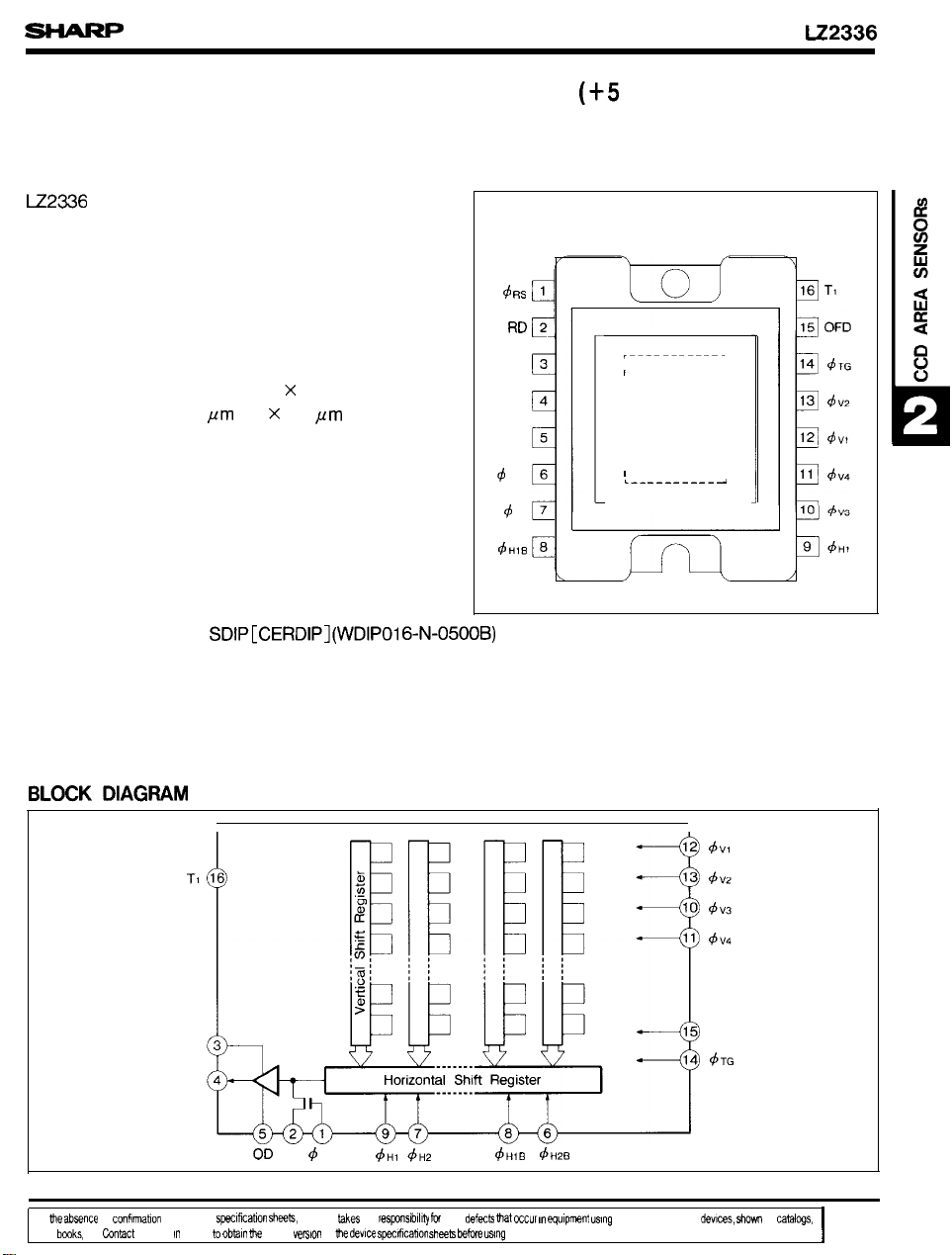
PIN CONNECTIONS
16-PIN SDIP
GND
0s
OD
H2B
H2
)
TOP VIEW
1
GND
0s
“In
abwnce of conf!mtlon by device swIflcation
dats bwks, etc
WARP
waler
obb[n
RD d ,S
WARP Wes no reswsib(llv
latest
of
swdlcabon shwh
any defeck hat quipmsnt
any SHARPs device
OFD
any of SHARP’s &vIces, zhom In
Page 2
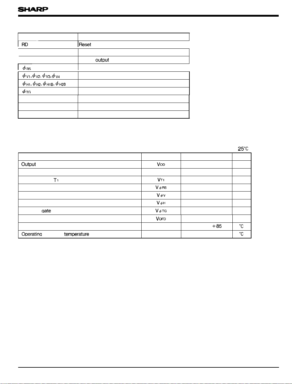
PIN DESCRIPTION
SYMBOL
Reset transistor drain
OD
0s Video
OFD
TI Test terminal
GND
Output transistor drain
Reset transistor gate clock
Vertical shift register gate clock
Horizontal shift register gate clock
Transfer gate clock
Overflow drain
Ground
LZ2336
PIN NAME
I
I
ABSOLUTE MAXIMUM RATINGS
PARAMETER
transistor drain voltage
Reset transistor drain voltage
Test terminal,
Reset sate clock voltage
Vertical shift register clock voltage
Horizontal shift register clock voltage
Transfer qate clock voltage
Overflow drain voltage Vom O to +27 v
Storage temperature
ambient
SYMBOL
RD
V
Tstg
Topr
RATING
Oto +15 v
Oto +15
Oto +15 v
–0.3 to +15 v
–0.3 to +15 v
–0.3 to +15 v
–0.3 to +15 v
–40 to
–20 to +70
(Ta =
)
UNIT
v
150
Page 3
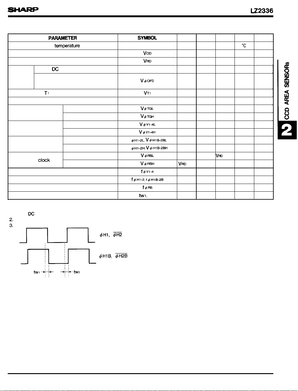
RECOMMENDED OPERATING CONDITIONS
Operating ambient
Output transistor drain voltage
Reset transistor drain voltage
Overflow
drain
voltage
Test terminal, TI
Ground voltage
Transfer gate clock
Vertical shift
register clock
Horizontal shift
register clock
Reset gate
Vertical shift register clock frequency
Horizontal shift register clock frequency
Reset gate clock frequency
Horizontal shift register clock phase
When
When pulse is applied
p-p level
is applied
LOW level
HIGH level
LOW level
HIGH level
LOW level
HIGH level
LOW level
HIGH level
V
v
MIN.
Topr 25.0 ‘c
Vom 3,0
GND
V+
–0.05
12.0
–
– 0.05
12.0
0,05
4.7
4.7
TYP. MAX.
12.5 14.0
Voo
12.0
12.5
VOD
14.0
0.0
0,05
0.0
12.5 14.0
0.05
0.0
5.0
0,0 0.05
5.0 6.0
6.0
0.0
-6.0 9.5 v
15.73 kHz
f+
6.75
6.75 MHz
0.0 5.0
10.0
UNIT
v
v
v
v
v
v
v
v
v
v
v
v
v
MHz
ns
NOTE
1
2
a
3
NOTES :
1. When
When pulse is applied, shutter speed is less than 1/60 seconds.
voltage is applied, shutter speed is 1/@ seconds.
151
Page 4

ELECTRICAL CHARACTERISTICS (Drive method : Field Accumulation)
temperature of light source : 3200 K /
PARAMETER SYMBOL
Photo response non-uniformity
Saturation signal
Dark output voltage
Dark signal non-uniformity
Sensitivity
Smear ratio SMR – 85 – 76
Image lag
Blooming suppression ratio
Output transistor drain current
Output impedance
.
standard output voltage is defined as 150
average output voltage under uniform illumination.
● The standard exposure level is defined when the average
output voltage is 150
NOTES :
1. Ta :
2. The image area is divided into 10x 10 segments. The segment’s voltage is the average output voltage of all the
pixels within the segment. PRNU is defined by (Vmax –
where Vmax and Vmin are the maximum and
the minimum values of each segment’s voltage respectively, when the average output voltage Vo is 150mV.
3. The image area is divided into 10x 10 segments.
The saturation signal is defined as the minimum of each
segment’s voltage which is the average output voltage of
all the pixels
is set as 10 times, compared to standard level,
4. The average output voltage under a non-exposure condition.
5. The image ~ea is
defined by
under uniform illumination.
the segment, when the exposure level
into 10x 10 segments. DSNU is
–
under the non-exposure con-
cut-off filter (CM-500, 1
PRNU
Vsat
Vdark
DSNU
R
Al
ABL
by the
dition where Vdmax and Vdmin are the maximum and the
minimum values of each segment’s voltage, respectively,
that is the average output voltage over all pixels in the
segment.
The average output voltage when a 10W ight source
6
attached with a
f50 mm.
7
The sensor is adjusted to
center of image area where V is the vertical length of the
image area, SMR is defined by the ratio of the output
voltage detected during the vertical blanking period to the
maximum of the pixel voltage in the V/l O square.
The sensor is exposed at the exposure level correspond-
8
ing to the standard condition preceding non-exposure condition. Al is defined by the ratio between the output voltage measured at the 1st field during the non-exposure
period and the standard output voltage.
The sensor is adjusted to position a V/l O square at the
9
center of image area. ABL is the ratio between the exposure at the standard condition and the exposure at a
point where a blooming is observed.
MIN.
TYP. MAX.
1.5
160 220
1000
400
reflector is imaged by a lens of F4,
UNIT NOTE
15
‘?/0
15.0
5.0
1.0
a V/l O square at the
2
3
1, 4
1, 5
6
7
8
9
Page 5
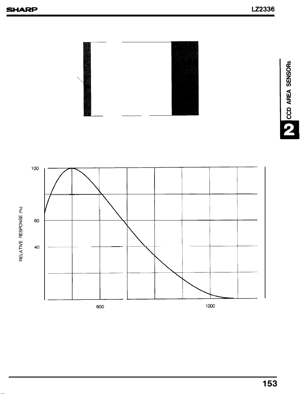
PIXEL STRUCTURE
SPECTRAL
80
OPTICAL BLACK
(2 PIXELS)
RESPONSE EXAMPLE
362
(H) X 492
(v)
OPTICAL BLACK
(20 PIXELS)
20
o
400
800
WAVE LENGTH
Wo
(rim)
1200
Page 6

TIMING DIAGRAM EXAMPLE
VERTICAL TRANSFER TIMING
(ODD FIELD)
HD
VD
0s
(EVEN FIELD)
VD
0s
525 1
n n n
I
u u u
n n nnnnn
n n
~+4a+6~+84~0 492
485487489491
II II
v
uuu
483485467489491
n
II
263
u uuu
&4;04;2
n
u u u uuu u
II
n
n
n
u
u
u
u u uuu u u
n n
nnn
n II
nnn
u u
10
u
272
u
n
nnn n
n n n
u uuu
u u u
n
n n
n n
n n
u u
u u u u u
17
n
u u
u
n
n
u
n
u u u u
u u
n
n n n
279
nnn n
u
n
n n
n
n n
n
n
u u
u
u uuu
n n
n
n
n
357911
246
8 10 12
II
n
n
uuu u u
u
u
n n
n
n
6810
nnn
u
n n
II
nnn
u
u u u
Il.
HD
es
0s
I
OB(20)
HORIZONTAL TRANSFER
I
TIMING
Page 7
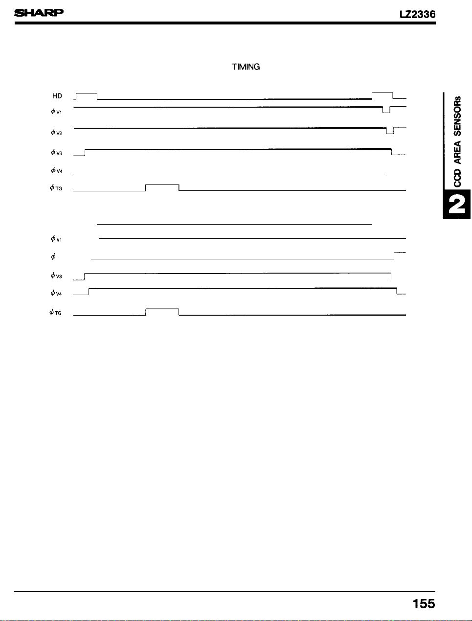
(ODD FIELD)
(EVEN FIELD)
HD
V2
READOUT
n
Page 8
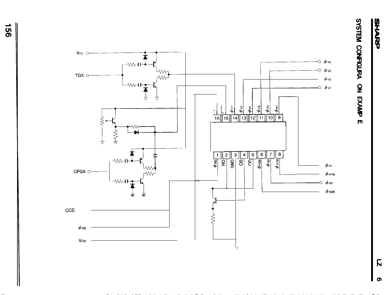
OUT O
O
LZ2336
I
I
o
o
 Loading...