

Page 1
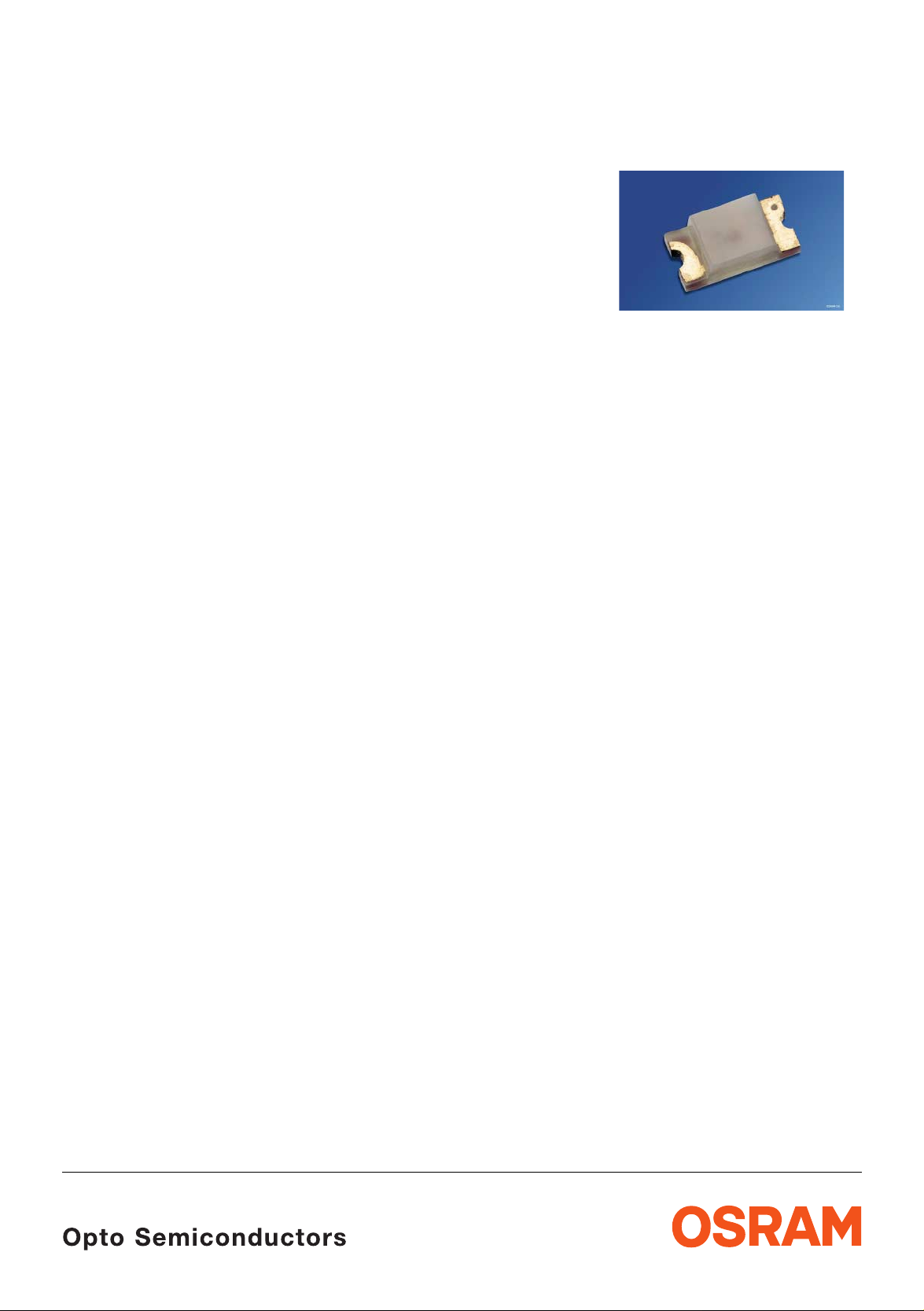
CHIPLED
LG N971, LY N971
Besondere Merkmale
• Gehäusetyp: 1206
• Besonderheit des Bauteils: extrem kleine
Bauform 3,2 mm x 1,6 mm x 1,1 mm
• Wellenlänge: 570 nm (grün), 587 nm (gelb)
• Abstrahlwinkel: Lambertscher Strahler (160°)
• Technologie: GaP (grün), GaAsP (gelb)
• optischer Wirkungsgrad: 2,5 lm/W (grün),
1,5 lm/W (gelb)
• Verarbeitungsmethode: für alle
SMT-Bestücktechniken geeignet
• Lötmethode: IR Reflow Löten
• Vorbehandlung: nach JEDEC Level 2
• Gurtung: 8 mm Gurt mit 3000/Rolle, ø180 mm
Anwendungen
• Informationsanzeigen im Innenbereich
• optischer Indikator
• Flache Hinterleuchtung (LCD, Handy,
Schalter, Display)
• Spielsachen
Features
• package: 1206
• feature of the device: extremely small
package 3.2 mm x 1.6 mm x 1.1 mm
• wavelength: 570 nm (green), 587 nm (yellow)
• viewing angle: Lambertian Emitter (160°)
• technology: GaP (green), GaAsP (yellow)
• optical efficiency: 2.5 lm/W (green),
1.5 lm/W (yellow)
• assembly methods: suitable for all
SMT assembly methods
• soldering methods: IR reflow soldering
• preconditioning: acc. to JEDEC Level 2
• taping: 8 mm tape with 3000/reel, ø180 mm
Applications
• indoor displays
• optical indicators
• flat backlighting (LCD, cellular phones,
switches, displays)
• toys
2002-04-05 1
Page 2
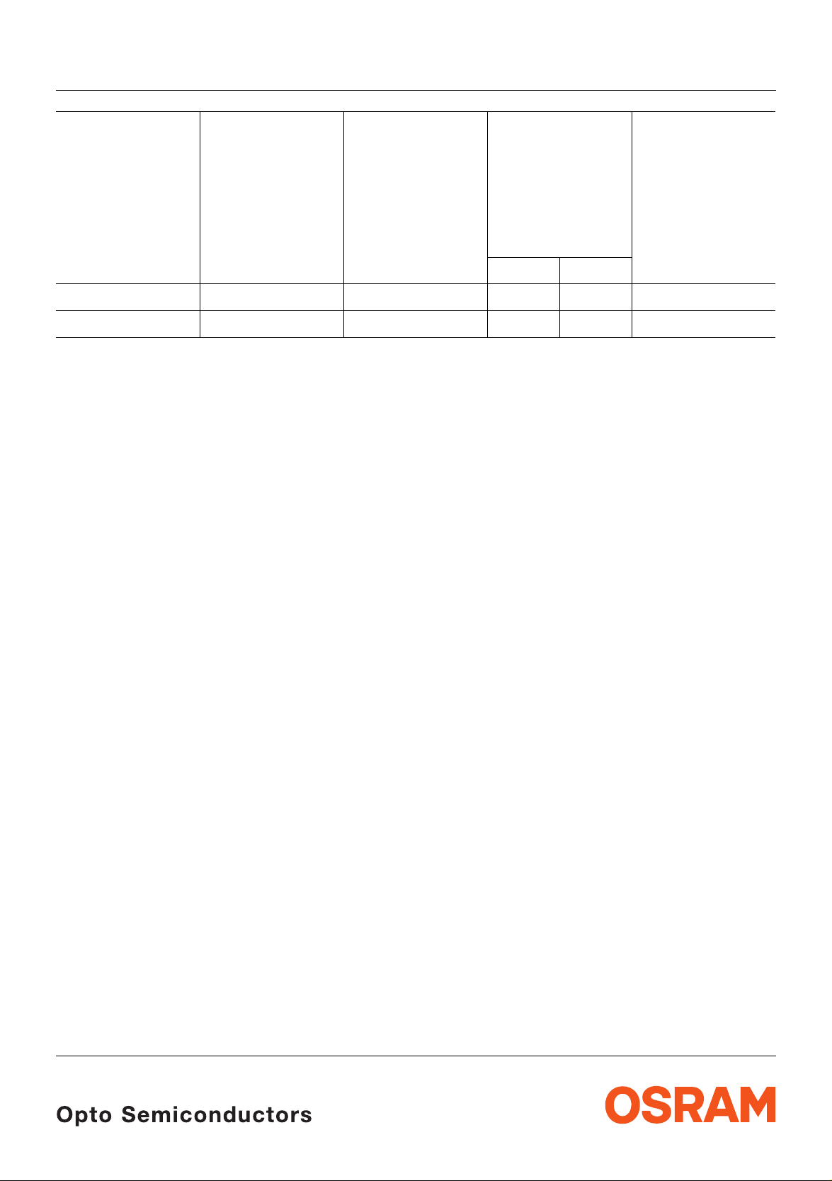
LG N971, LY N971
Typ
Emissionsfarbe
Farbe der
Lichtstärke
Bestellnummer
Lichtaustrittsfläche
Type
Color of
Emission
Color of the
Light Emitting
Area
Luminous
Intensity
I
= 20 mA
F
I
(mcd)
V
Ordering Code
min. typ.
LG N971 green colorless diffused 7.1 10 Q62702-P5191
LY N971 yellow colorless diffused 2.8 6 Q62702-P5193
Helligkeitswerte werden m it einer Stromeinprägedauer von 25 ms und einer Genauigkeit von ±11 % ermittelt.
Luminous intensity is tested at a current pulse duration of 25 ms and a tolerance of ±11 %.
Anm.: Die Standardlieferform von Serientypen beinhaltet alle Gruppen. Einzelne Gruppen sind nicht
erhältlich.
In einer Verpackungseinheit / Gurt ist immer nur eine Gruppe enthalten.
Note: The standard shipping format for serial types includes all groups. Individual groups are not
available.
No packing unit / tape ever contains more than one luminous intensity group.
2002-04-05 2
Page 3
Grenzwerte
Maximum Ratings
LG N971, LY N971
Bezeichnung
Parameter
Betriebstemperatur
Operating temperature range
Lagertemperatur
Storage temperature range
Sperrschichttemperatur
Junction temperature
Durchlassstrom
Forward current
Stoßstrom
Surge current
t
= 10 µs, D = 0.1
p
Sperrspannung
Reverse voltage
Leistungsaufnahme
Power consumption
Wärmewiderstand
Thermal resistance
Sperrschicht/Umgebung
Junction/ambient
Sperrschicht/Lötpad
Junction/solder point
Montage auf PC-Board FR 4 (Padgröße
mounted on PC board FR 4 (pad size
≥ 5mm
≥ 5mm
2
)
2
)
Symbol
Symbol
T
op
T
stg
T
j
I
F
I
FM
V
R
P
tot
R
th JA
R
th JS
Wert
Value
Einheit
Unit
– 30 … + 85 °C
– 40 … + 85 °C
+ 95 °C
25 (green)
mA
20 (yellow)
0.1 A
5V
65 mW
750
430
K/W
K/W
2002-04-05 3
Page 4

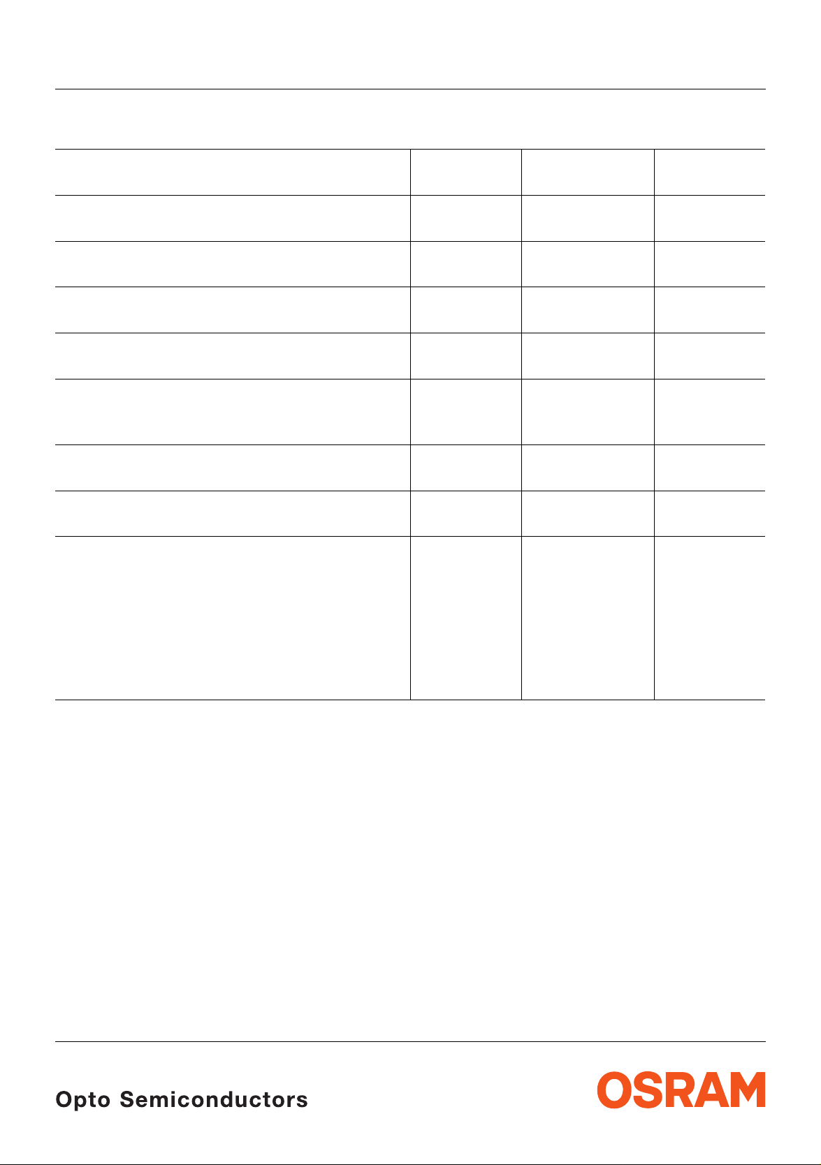
Kennwerte (TA = 25 °C)
Characteristics
LG N971, LY N971
Bezeichnung
Parameter
Symbol
Symbol
Werte
Values
Einheit
Unit
LG LY
Wellenlänge des emittierten Lichtes (typ.)
λ
peak
572 589 nm
Wavelength at peak emission
I
= 20 mA
F
Dominantwellenlänge
Dominant wavelength
I
= 20 mA
F
Spektrale Bandbreite (typ.)
1)
1)
(typ.)
λ
dom
570 587 nm
∆λ 30 40 nm
Spectral bandwidth
I
= 20 mA
F
Abstrahlwinkel bei 50 %
Viewing angle at 50 %
Durchlassspannung
Forward voltage
I
= 20 mA
F
2)
Sperrstrom (typ.)
Reverse current (max.)
V
= 5 V
R
Temperaturkoeffizient von
Temperature coefficient of
I
=20 mA; –10°C ≤ T ≤ 100°C
F
Temperaturkoeffizient von
Temperature coefficient of
I
= 20 mA; –10°C ≤ T ≤ 100°C
F
Temperaturkoeffizient von
Temperature coefficient of
I
= 20 mA; –10°C ≤ T ≤ 100°C
F
Optischer Wirkungsgrad (typ.)
I
(Vollwinkel) (typ.)
V
I
V
2)
λ
peak
λ
peak
λ
dom
λ
dom
V
F
V
F
(typ.)
(max.)
(typ.)
(typ.)
(typ.)
2ϕ 160 160 Grad
deg.
V
V
I
R
I
R
TC
TC
TC
η
opt
F
F
λpeak
λdom
V
2.2
2.6
0.02
100
2.2
2.6
0.02
100
V
V
µA
µA
0.10 0.11 nm/K
0.06 0.08 nm/K
– 1.4 – 1.7 mV/K
2.5 1.5 lm/W
Optical efficiency
I
= 20 mA
F
1)
Wellenlängengruppen werden mit einer Stromeinprägedauer von 25 ms und einer Genauigkeit von ±1 nm ermittelt.
Wavelength groups are tested at a current pulse duration of 25 ms and a tolerance of ±1 nm.
2)
Spannungswerte werde n mit einer Stromeinprägedauer von 1 ms und einer Genauigkeit von ±0,1 V ermittelt.
Voltages are tested at a curre nt puls e duration of 1 ms and a tolerance of ±0.1 V.
2002-04-05 4
Page 5

LG N971, LY N971
Relative spektrale Emission I
rel
Relative Spectral Emission
λ) = spektrale Augenempfindlichkeit
V(
Standard eye response curve
100
%
I
rel
80
60
40
20
= f (λ), TA = 25 °C, IF = 20 mA
V
λ
green yellow
OHL00406
0
400
Abstrahlcharakteristik
Radiation Characteristic
50˚
60˚
70˚
80˚
90˚
450 500 550 600 650 700
nm
λ
I
= f (ϕ)
rel
0˚10˚20˚40˚ 30˚
ϕ
1.0
0.8
0.6
0.4
0.2
0
OHL00408
100˚
1.0 0.8 0.6 0.4
2002-04-05 5
0˚ 20˚ 40˚ 60˚ 80˚ 100˚ 120˚
Page 6

LG N971, LY N971
Durchlassstrom IF = f (VF)
Forward Current
T
= 25 °C
A
2
10
mA
I
1
F
10
0
10
-1
10
-2
10
-3
10
1
1.4 1.8 2.2 2.6 3 3.4
OHL00636
greenyellow
V
V
F
Maximal zulässiger Durchlassstrom
Max. Permissible Forward Current
40
mA
35
I
F
30
OHL00637
I
= f (TA)
F
Relative Lichtstärke
I
V/IV(20 mA)
Relative Luminous Intensity
T
= 25 °C
A
1
10
I
V
I
V
(20 mA)
0
10
5
-1
10
5
-2
10
-1 0
10
Relative Lichtstärke
10 10
55
I
V/IV(25 °C)
Relative Luminous Intensity
I
= 20 mA
F
2
I
V
I
V
(25 ˚C)
1.6
= f (IF)
OHL00426
12
mA
10
I
F
= f (TA)
OHL01094
25
green
20
yellow
T
S
T
A
15
10
5
0
0
temp. ambient
T
A
temp. solder point
T
S
20 40 60 80 100
˚C
T
2002-04-05 6
yellow
1.2
green
0.8
0.4
0
-20 0 20 40 60 ˚C 100
T
A
Page 7

Maßzeichnung
Package Outlines
LG N971, LY N971
ø0.7 (ø0.028)
ø0.5 (ø0.020)
Cathode
mark
1.7 (0.067)
1.5 (0.059)
3.1 (0.122)
3.3 (0.130)
1.2 (0.047)
1.0 (0.039)
0.6 (0.024)
0.4 (0.016)
2.1 (0.083)
1.9 (0.075)
2.1 (0.083)
1.9 (0.075)
0.6 (0.024)
0.4 (0.016)
Cathode
mark
Polarity
Soldering terminal
may flow in x, y direction
GEOY6008
Maße werden wie folgt angegeb en: m m (inch) / Dimensions are specified as follo w s: m m (inc h).
Gewicht / Approx. weight: 7.5 mg
2002-04-05 7
Page 8

Lötbedingungen Vorbehandlung nach JEDEC Level 2
Soldering Conditions Preconditioning acc. to JEDEC Level 2
IR-Reflow Lötprofil (nach IPC 9501)
IR Reflow Soldering Profile (acc. to IPC 9501)
LG N971, LY N971
250
˚C
T
200
150
100
50
0
0:00
2-3 K/s
0:30 1:00 1:30 2:00 2:30 3:00 3:30 4:00 4:30 5:00 5:30
T
= 183 ˚C = 70 s
t
T
max
= 245 ˚C
2-3 K/s
OHLA0685
min
t
2002-04-05 8
Page 9

Empfohlenes Lötpaddesign IR Reflow Löten
Recommended Solder Pad IR Reflow Soldering
LG N971, LY N971
1.5 (0.059)
1.5 (0.059) 2.0 (0.079)
Maße werden wie folgt angegeb en: m m (inch) / Dimensions are specified as follo w s: m m (inc h).
1.5 (0.059)
OHAPY608
Gurtung / Polarität und Lage Verpackungseinheit 3000/Rolle, ø180 mm
Method of Taping / Polarity and Orientation Packing unit 3000/reel, ø180 mm
Processive Direction
1.5 (0.059)
Cathode mark
(2.1 (0.083))
4 (0.157)
4 (0.157)
2 (0.079)
1.75 (0.069)
3.5 (0.138)
3.75 (0.148)
C
8 (0.315)
A
OHAY0529
Maße werden wie folgt angegeb en: m m (inch) / Dimensions are specified as follo w s: m m (inc h).
2002-04-05 9
Page 10

Revision History: 2002-04-05
Previous Version: 2001-03-05
Page Subjects (major changes since last revision)
7 cathode marking
4forward voltage
4 wavelength yellow
3 pad size from 16 mm
2
to 5 mm
2
LG N971, LY N971
Published by OSRAM Opto Semiconductors GmbH & Co. OHG
Wernerwerkstrasse 2, D-93049 Regensburg
© All Rights Reserved.
Attention please!
The information describes the type of component and shall not be considered as assured char ac te ris tics .
Terms of delivery and rights to change design reserved. Due to technical requirements components may contain
dangerous substances. For information on the types in question please contact our Sales Organization.
If printed or downloaded, please find the latest version in the Internet .
Packing
Please use the recycling operators k nown to you . We can als o help you – get in touch wit h your near est sales offic e.
By agreement we will take p acking material back, if it is sorted. You m ust bear the costs of transport. For packing
material that is returned to us unsorted or which we are not obliged to accept, we shall have to invoice you for any costs
incurred.
Components used in life-support devices or systems must be expressly authorized for such purpose! Critical
components
1
A critical component is a co mponent used in a life -support device or syst em whose failure ca n reasonably be expecte d
to cause the failure of that life-support device or system, or to affect its safety or the effectiveness of that device or
system.
2
Life support devices or systems are intend ed (a) to be impl anted i n t he human b ody , or (b ) to supp ort a nd/or ma inta in
and sustain human life. If th ey fail , it is rea so nable to assume that the health of the us er m ay be endangered.
2002-04-05 10
1
may only be used in life-support dev ic es or sys t em s 2 with the express written approval of OSRAM OS.
 Loading...