

Page 1
MINI HOME THEATER
SERVICE MANUAL
P/N : AFN30086058 APRIL, 2006
MODELS:
LX-D2560 (LXS-D2560V)
LX-D2960 (LXS-D2960V)
LX-D3960 (LXS-D3960W, D3960V)
KR-2500DV (LXS-D3960W, D3960V)
LX-D6960 (LXS-D6960W, D6960V, D6960C, D6960T)
KR-5550DV (LXS-D6960W, D6960V, D6960C, D6960T)
LX-K4960 (LXS-K4960W, K4960V)
LX-K7960 (LXS-K7960W, K7960V, K7960C, K7960T)
LF-K3560Q (LF-K3560, K3560V)
LF-K3565Q (LF-K3565, K3565V)
LF-K3960Q (LF-K3960, K3960V)
SERVICE MANUAL MODELS: LX-D2560, LX-D2960, LX-D3960, KR-2500DV, LX-D6960, KR-5550DV, LX-K4960, LX-K7960, LF-K3560Q, LF-K3565Q, LF-K3960Q
CAUTION
BEFORE SERVICING THE UNIT, READ THE “SAFETY PRECAUTIONS” IN THIS MANUAL.
Page 2

- 1-1 -
[CONTENTS]
❍ SECTION 1. GENERAL
• SERVICING PRECAUTIONS . . . . . . . . . . . . . . . . . . . . . . . . . . . . . . . . . . . . . . . . . . . . . . . 1-2
• ESD PRECAUTIONS . . . . . . . . . . . . . . . . . . . . . . . . . . . . . . . . . . . . . . . . . . . . . . . . . . . . . 1-4
• SPECIFICATION . . . . . . . . . . . . . . . . . . . . . . . . . . . . . . . . . . . . . . . . . . . . . . . . . . . . . . . . . .1-5
❍ SECTION 2. EXPLODED VIEWS
1. CABINET AND MAIN FRAME SECTION . . . . . . . . . . . . . . . . . . . . . . . . . . . . . . . . . . . . . . 2-1
2. DECK MECHANISM EXPLODED VIEW (5 CHANGER) . . . . . . . . . . . . . . . . . . . . . . . . . . . 2-3
3. TAPE DECK MECHANISM . . . . . . . . . . . . . . . . . . . . . . . . . . . . . . . . . . . . . . . . . . . . . . . . 2-5
❍ SECTION 3. ELECTRICAL SECTION
• ELECTRICAL TROUBLESHOOTING GUIDE . . . . . . . . . . . . . . . . . . . . . . . . . . . . . . . . . . . .3-1
• INTERNAL BLOCK DIAGRAM of ICs . . . . . . . . . . . . . . . . . . . . . . . . . . . . . . . . . . . . . . . . .3-13
• WIRING DIAGRAM . . . . . . . . . . . . . . . . . . . . . . . . . . . . . . . . . . . . . . . . . . . . . . . . . . . . . . .3-25
• BLOCK DIAGRAM . . . . . . . . . . . . . . . . . . . . . . . . . . . . . . . . . . . . . . . . . . . . . . . . . . . . . . .3-27
• SCHEMATIC DIAGRAMS . . . . . . . . . . . . . . . . . . . . . . . . . . . . . . . . . . . . . . . . . . . . . . . . . .3-29
• PRINTED CIRCUIT DIAGRAMS . . . . . . . . . . . . . . . . . . . . . . . . . . . . . . . . . . . . . . . . . . . . .3-41
❍ SECTION 4. DVD PART ELECTRICAL
• DVD ELECTRICAL TROUBLESHOOTIHG GUIDE . . . . . . . . . . . . . . . . . . . . . . . . . . . . . . . .4-1
• DVD SCHEMATIC DIAGRAMS . . . . . . . . . . . . . . . . . . . . . . . . . . . . . . . . . . . . . . . . . . . . . .4-15
• DVD PRINTED CIRCUIT DIAGRAMS . . . . . . . . . . . . . . . . . . . . . . . . . . . . . . . . . . . . . . . . .4-23
❍ SECTION 5. MECHANISM OF DVD PART
• DECK MECHANISM DISASSEMBLY . . . . . . . . . . . . . . . . . . . . . . . . . . . . . . . . . . . . . . . . . .5-1
• EXPLODED VIEW . . . . . . . . . . . . . . . . . . . . . . . . . . . . . . . . . . . . . . . . . . . . . . . . . . . . . . . .5-7
❍ SECTION 6. REPLACEMENT PARTS LIST
• REPLACEMENT PARTS LIST . . . . . . . . . . . . . . . . . . . . . . . . . . . . . . . . . . . . . . . . . . . . . . . .6-1
Page 3
- 1-2 -
SECTION 1. GENERAL
❏ SERVICING PRECAUTIONS
■ NOTES REGARDING HANDLING OF THE PICK-UP
1. Notes for transport and storage
1) The pick-up should always be left in its conductive bag until immediately prior to use.
2) The pick-up should never be subjected to external pressure or impact.
2. Repair notes
1) The pick-up incorporates a strong magnet, and so should never be brought close to magnetic materials.
2) The pick-up should always be handled correctly and carefully, taking care to avoid external pressure and
impact. If it is subjected to strong pressure or impact, the result may be an operational malfunction and/or
damage to the printed-circuit board.
3) Each and every pick-up is already individually adjusted to a high degree of precision, and for that reason
the adjustment point and installation screws should absolutely never be touched.
4) Laser beams may damage the eyes!
Absolutely never permit laser beams to enter the eyes!
Also NEVER switch ON the power to the laser output part (lens, etc.) of the pick-up if it is damaged.
5) Cleaning the lens surface
If there is dust on the lens surface, the dust should be cleaned away by using an air bush (such as used
for camera lens). The lens is held by a delicate spring. When cleaning the lens surface, therefore, a cotton
swab should be used, taking care not to distort this.
6) Never attempt to disassemble the pick-up.
Spring by excess pressure. If the lens is extremely dirty, apply isopropyl alcohol to the cotton swab. (Do
not use any other liquid cleaners, because they will damage the lens.) Take care not to use too much of
this alcohol on the swab, and do not allow the alcohol to get inside the pick-up.
Storage in conductive bag
Drop impact
NEVER look directly at the laser beam, and don’t let
contact fingers or other exposed skin.
Magnet
How to hold the pick-up
Conductive Sheet
Cotton swab
Pressure
Pressure
Page 4
- 1-3 -
■ NOTES REGARDING COMPACT DISC PLAYER REPAIRS
1. Preparations
1) Compact disc players incorporate a great many ICs as well as the pick-up (laser diode). These components
are sensitive to, and easily affected by, static electricity. If such static electricity is high voltage, components
can be damaged, and for that reason components should be handled with care.
2) The pick-up is composed of many optical components and other high-precision components. Care must be
taken, therefore, to avoid repair or storage where the temperature of humidity is high, where strong magnetism is present, or where there is excessive dust.
2. Notes for repair
1) Before replacing a component part, first disconnect the power supply lead wire from the unit
2) All equipment, measuring instruments and tools must be grounded.
3) The workbench should be covered with a conductive sheet and grounded.
When removing the laser pick-up from its conductive bag, do not place the pick-up on the bag. (This is
because there is the possibility of damage by static electricity.)
4) To prevent AC leakage, the metal part of the soldering iron should be grounded.
5) Workers should be grounded by an armband (1M Ω)
6) Care should be taken not to permit the laser pick-up to come in contact with clothing, in order to prevent static electricity changes in the clothing to escape from the armband.
7) The laser beam from the pick-up should NEVER be directly facing the eyes or bare skin.
CLEARING MALFUNCTION
You can reset your unit to initial status if malfunction occur(button malfunction, display, etc.).
Using a pointed good conductor(such as driver), simply short the RESET jump wire on the inside of
the volume knob for more than 3 seconds.
If you reset your unit, you must reenter all its settings(stations, clock, timer)
NOTE: 1.To operate the RESET jump wire, pull the volume rotary knob and release it.
2. If you wish to operate the RESET jump wire, it is necessary to unplug the power cord.
Resistor
(1 Mohm)
Conductive
Sheet
Resistor
(1 Mohm)
Armband
RESET jump wire
VOLUME
VOLUME KNOB
DOWN
UP
Page 5
- 1-4 -
❏ ESD PRECAUTIONS
■ Electrostatically Sensitive Devices (ESD)
Some semiconductor (solid state) devices can be damaged easily by static electricity. Such components
commonly are called Electrostatically Sensitive Devices (ESD). Examples of typical ESD devices are integrated
circuits and some field-effect transistors and semiconductor chip components.The following techniques should
be used to help reduce the incidence of component damage caused by static electricity.
1. Immediately before handling any semiconductor component or semiconductor-equipped assembly, drain off
any electrostatic charge on your body by touching a known earth ground. Alternatively, obtain and wear a
commercially available discharging wrist strap device, which should be removed for potential shock reasons
prior to applying power to the unit under test.
2. After removing an electrical assembly equipped with ESD devices, place the assembly on a conductive sur-
face such as aluminum foil, to prevent electrostatic charge buildup or exposure of the assembly.
3. Use only a grounded-tip soldering iron to solder or unsolder ESD devices.
4. Use only an anti-static solder removal device. Some solder removal devices not classified as "anti-static" can
generate electrical charges sufficient to damage ESD devices.
5. Do not use freon-propelled chemicals. These can generate electrical charges sufficient to damage ESD
devices.
6. Do not remove a replacement ESD device from its protective package until immediately before you are
ready to install it. (Most replacement ESD devices are packaged with leads electrically shorted together by
conductive foam, aluminum foil or comparable conductive materials).
7. Immediately before removing the protective material from the leads of a replacement ESD device, touch the
protective material to the chassis or circuit assembly into which the device will by installed.
CAUTION : BE SURE NO POWER IS APPLIED TO THE CHASSIS OR CIRCUIT, AND OBSERVE ALL
OTHER SAFETY PRECAUTIONS.
8. Minimize bodily motions when handing unpackaged replacement ESD devices. (Otherwise harmless motion
such as the brushing together of your clothes fabric or the lifting of your foot from a carpeted floor can generate static electricity sufficient to damage an ESD device).
CAUTION. GRAPHIC SYMBOLS
THE LIGHTNING FLASH WITH APROWHEAD SYMBOL. WITHIN AN EQUILATERAL TRIANGLE, IS
INTENDED TO ALERT THE SERVICE PERSONNEL TO THE PRESENCE OF UNINSULATED “DAN-
GEROUS VOLTAGE” THAT MAY BE OF SUFFICIENT MAGNITUDE TO CONSTITUTE A RISK OF
ELECTRIC SHOCK.
THE EXCLAMATION POINT WITHIN AN EQUILATERAL TRIANGLE IS INTENDED TO ALERT THE
SERVICE PERSONNEL TO THE PRESENCE OF IMPORTANT SAFETY INFORMATION IN SERVICE
LITERATURE.
Page 6

- 1-5 -
❏ SPECIFICATIONS
MODELS: LX-K4960, LX-D3960, KR-2550DV
LX-K4960A, LXS-K4960V, LXS-K4960W
LX-D3960A, LXS-D3960V, LXS-D3960W
General
Power supply Refer to the main label.
Power consumption 70 W
Net Weight 5.9 kg
External dimensions (W x H x D) 190 X 352 X 295 mm
Tuner/Amplifier
FM Tuning Range 87.5 - 108.0 MHz or 65 -74 MHz, 87.5 -108.0 MHz
Intermediate Frequency 10.7 MHz
Signal to Noise Ratio 60/55 dB (Mono/Stereo)
Frequency Response 50 - 10000 Hz
AM Tuning Range 522 - 1620 kHz or 520 - 1720 kHz
Intermediate Frequency 450 kHz
Signal to Noise Ratio 30 dB
Frequency Response 140 - 1800 Hz
Output Power Front: 100 W + 100 W (4 Ω , THD 10 %)
Sub woofer: 150 W (3 Ω , THD 10 %)
T.H.D 0.5 %
Frequency Response 40 - 20000 Hz
Signal-to-noise ratio 75 dB
DVD/VCD/CD player
Frequency response (audio) 40 - 20000 Hz
Signal-to-noise ratio (audio) More than 75 dB (1 kHz)
Signal-to-noise ratio (video) More than 55 dB (1 kHz)
Dynamic range (audio) More than 80 dB
Video output 1.0 V (p-p), 75 Ω
S-video output (Y) 1.0 V (p-p), 75 Ω
(C) 0.3 V (p-p), 75 Ω
Component Video output (Y) 1.0 V (p-p), 75 Ω
(Pb)/(Pr) 0.7 V (p-p), 75 Ω
Speakers
Speaker Name Front Speaker (L/R) Subwoofer
Type
Bass Reflex 2Way 3Speaker Bass Reflex 1Way 1Speaker
Impedance 4 Ω 3 Ω
Frequency Response 60 - 20000 Hz 50 - 20000 Hz
Sound Pressure Level 85 dB/W (1m) 82 dB/W (1m)
Rated Input Power 100 W 150 W
Max. Input Power 200 W 300 W
Net Dimensions (W x H x D) 190 X 351 X 295 mm 190 X 351 X 295 mm
Net Weight 4.8 kg 4.9 kg
Cassette tape player
Tape Speed 3000 ± 3 % (MTT-111.
NORMAL-SPEED)
Wow Flutter 0.25 %
(TT -111, JIS-WTD)
F.F/REW. Time 120 sec (C-60)
Frequency Response 250 - 8000 Hz
Signal to Noise Ratio 43 dB
Channel Separation 50 dB (P/B)/45 dB (R/P)
Erase Ratio 55 dB (MTT-5511)
Page 7

- 1-6 -
MODELS: LF-K3960Q (LF-K3960, LFS-K3960V)
LF-K3565Q (LF-K3565, LFS-K3565V)
LF-K3560Q (LF-K3560, LFS-K3560V)
General
Power supply Refer to the main label.
Power consumption 70 W (LF-K3960Q Model)
50 W (LF-K3565Q/LF-K3560Q Model)
Net Weight 5.9 kg
External dimensions (W x H x D) 190 X 352 X 295 mm
Tuner/Amplifier
FM Tuning Range 87.5 - 108.0 MHz or 65 -74 MHz, 87.5 -108.0 MHz
Intermediate Frequency 10.7 MHz
Signal to Noise Ratio 60/55 dB (Mono/Stereo)
Frequency Response 50 - 10000 Hz
AM Tuning Range 522 - 1620 kHz or 520 - 1720 kHz
Intermediate Frequency 450 kHz
Signal to Noise Ratio 30 dB
Frequency Response 140 - 1800 Hz
Output Power Front: 100 W + 100 W (4 Ω, THD 10 %) - LF-K3960Q model
Front: 50 W + 50 W (4 Ω, THD 10 %) - LF-K3565Q/LF-K3560Q model
T.H.D 0.5 %
Frequency Response 40 - 20000 Hz
Signal-to-noise ratio 75 dB
DVD/VCD/CD player
Frequency response (audio) 40 - 20000 Hz
Signal-to-noise ratio (audio) More than 75 dB (1 kHz)
Signal-to-noise ratio (video) More than 55 dB (1 kHz)
Dynamic range (audio) More than 80 dB
Video output 1.0 V (p-p), 75 Ω
S-video output (Y) 1.0 V (p-p), 75 Ω
(C) 0.3 V (p-p), 75 Ω
Component Video output (Y) 1.0 V (p-p), 75 Ω
(Pb)/(Pr) 0.7 V (p-p), 75 Ω
Speakers
Speaker Name Front Speaker (L/R)
Type Bass Reflex 2Way 3Speaker (LF-K3960Q Model)
Bass Reflex 2Way 2Speaker (LF-K3565Q/LF-K3560Q Model)
Impedance 4 Ω
Frequency Response 60 - 20000 Hz
Sound Pressure Level 85 dB/W (1m)
Rated Input Power 100 W (LFS-K3960V)
50 W (LFS-K3565V/LFS-K3560V)
Max. Input Power 200 W (LFS-K3960V)
100 W (LFS-K3565V/LFS-K3560V)
Net Dimensions (W x H x D) 190 X 351 X 295 mm (LFS-K3960V)
190 X 351 X 270 mm (LFS-K3565V/LFS-K3560V)
Net Weight 4.8 kg (LFS-K3960V)
4.2 kg (LFS-K3565V/LFS-K3560V)
Cassette tape player
Tape Speed 3000 ± 3 % (MTT-111.
NORMAL-SPEED)
Wow Flutter 0.25 %
(TT -111, JIS-WTD)
F.F/REW. Time 120 sec (C-60)
Frequency Response 250 - 8000 Hz
Signal to Noise Ratio 43 dB
Channel Separation 50 dB (P/B)/45 dB (R/P)
Erase Ratio 55 dB (MTT-5511)
Page 8

- 1-7 -
MODELS: LX-D2960 (LX-D2960A, LXS-D2960V)
LX-D2560 (LX-D2560A, LXS-D2560V)
General
Power supply Refer to the main label.
Power consumption 70 W (LX-D2960A model)
50 W (LX-D2560A model)
Net Weight 5.9 kg
External dimensions (W x H x D) 190 X 352 X 295 mm
Tuner/Amplifier
FM Tuning Range 87.5 - 108.0 MHz or 65 -74 MHz, 87.5 -108.0 MHz
Intermediate Frequency 10.7 MHz
Signal to Noise Ratio 60/55 dB (Mono/Stereo)
Frequency Response 50 - 10000 Hz
AM Tuning Range 522 - 1620 kHz or 520 - 1720 kHz
Intermediate Frequency 450 kHz
Signal to Noise Ratio 30 dB
Frequency Response 140 - 1800 Hz
Output Power Front: 100 W + 100 W (4 Ω, THD 10 %) - LX-D2960A model
Front: 50 W + 50 W (4 Ω, THD 10 %) - LX-D2560A model
T.H.D 0.5 %
Frequency Response 40 - 20000 Hz
Signal-to-noise ratio 75 dB
DVD/VCD/CD player
Frequency response (audio) 40 - 20000 Hz
Signal-to-noise ratio (audio) More than 75 dB (1 kHz)
Signal-to-noise ratio (video) More than 55 dB (1 kHz)
Dynamic range (audio) More than 80 dB
Video output 1.0 V (p-p), 75 Ω
S-video output (Y) 1.0 V (p-p), 75 Ω
(C) 0.3 V (p-p), 75 Ω
Component Video output (Y) 1.0 V (p-p), 75 Ω
(Pb)/(Pr) 0.7 V (p-p), 75 Ω
Speakers
Speaker Name Front Speaker (L/R)
Type Bass Reflex 2Way 3Speaker (LXS-D2960V Model)
Bass Reflex 2Way 2Speaker (LXS-D2560V Model)
Impedance 4 Ω
Frequency Response 60 - 20000 Hz
Sound Pressure Level 85 dB/W (1m)
Rated Input Power 100 W (LXS-D2960V)
50 W (LXS-D2560V)
Max. Input Power 200 W (LXS-D2960V)
100 W (LXS-D2560V)
Net Dimensions (W x H x D) 190 X 351 X 295 mm (LXS-D2960V)
190 X 351 X 270 mm (LXS-D2560V)
Net Weight 4.8 kg (LXS-D2960V)
4.2 kg (LXS-D2560V)
Cassette tape player
Tape Speed 3000 ± 3 % (MTT-111.
NORMAL-SPEED)
Wow Flutter 0.25 %
(TT -111, JIS-WTD)
F.F/REW. Time 120 sec (C-60)
Frequency Response 250 - 8000 Hz
Signal to Noise Ratio 43 dB
Channel Separation 50 dB (P/B)/45 dB (R/P)
Erase Ratio 55 dB (MTT-5511)
Page 9

- 1-8 -
MODELS: LX-K7960, LX-D6960, KR-5550DV
LX-K7960A
LXS-K7960V, LXS-K7960C, LXS-K7960T, LXS-K7960W
LX-D6960A,D
LXS-D6960V, LXS-D6960C, LXS-D6960T, LXS-D6960W
General
Power supply Refer to the main label.
Power consumption 90 W
Net Weight 5.9 kg
External dimensions (W x H x D) 190 X 352 X 295 mm
Tuner/Amplifier
FM Tuning Range 87.5 - 108.0 MHz or 65 -74 MHz, 87.5 -108.0 MHz
Intermediate Frequency 10.7 MHz
Signal to Noise Ratio 60/55 dB (Mono/Stereo)
Frequency Response 50 - 10000 Hz
AM Tuning Range 522 - 1620 kHz or 520 - 1720 kHz
Intermediate Frequency 450 kHz
Signal to Noise Ratio 30 dB
Frequency Response 140 - 1800 Hz
Output Power Front: 100 W + 100 W (4 Ω, THD 10 %), Center: 50 W (8 Ω, THD 10%)
Rear: 50 W + 50 W (8 Ω, THD 10 %), Sub woofer: 150 W (3 Ω, THD 10 %)
T.H.D 0.5 %
Frequency Response 40 - 20000 Hz
Signal-to-noise ratio 75 dB
DVD/VCD/CD player
Frequency response (audio) 40 - 20000 Hz
Signal-to-noise ratio (audio) More than 75 dB (1 kHz)
Signal-to-noise ratio (video) More than 55 dB (1 kHz)
Dynamic range (audio) More than 80 dB
Video output 1.0 V (p-p), 75 Ω
S-video output (Y) 1.0 V (p-p), 75 Ω
(C) 0.3 V (p-p), 75 Ω
Component Video output (Y) 1.0 V (p-p), 75 Ω
(Pb)/(Pr) 0.7 V (p-p), 75 Ω
Speakers
Speaker Name Front Speaker (L/R) Center Speaker
Type
Bass Reflex 2Way 3Speaker Bass Reflex 2Way 3Speaker
Impedance 4 Ω 8 Ω
Frequency Response 60 - 20000 Hz 150 - 20000 Hz
Sound Pressure Level 85 dB/W (1m) 85 dB/W (1m)
Rated Input Power 100 W 50 W
Max. Input Power 200 W 100 W
Net Dimensions (W x H x D) 190 X 351 X 295 mm 300 X 109 X 115 mm
Net Weight 4.8 kg 1.3 kg
Speaker Name Rear Speaker (L/R) Subwoofer
Type
Bass Reflex 1Way 1Speaker Bass Reflex 1Way 1Speaker
Impedance 8 Ω 3 Ω
Frequency Response 150 - 20000 Hz 50 - 20000 Hz
Sound Pressure Level 85 dB/W (1m) 82 dB/W (1m)
Rated Input Power 50 W 150 W
Max. Input Power 100 W 300 W
Net Dimensions (W x H x D) 100 X 354 X 117 mm 190 X 351 X 295 mm
Net Weight 0.9 kg 4.9 kg
Cassette tape player
Tape Speed 3000 ± 3 % (MTT-111.
NORMAL-SPEED)
Wow Flutter 0.25 %
(TT -111, JIS-WTD)
F.F/REW. Time 120 sec (C-60)
Frequency Response 250 - 8000 Hz
Signal to Noise Ratio 43 dB
Channel Separation 50 dB (P/B)/45 dB (R/P)
Erase Ratio 55 dB (MTT-5511)
Page 10
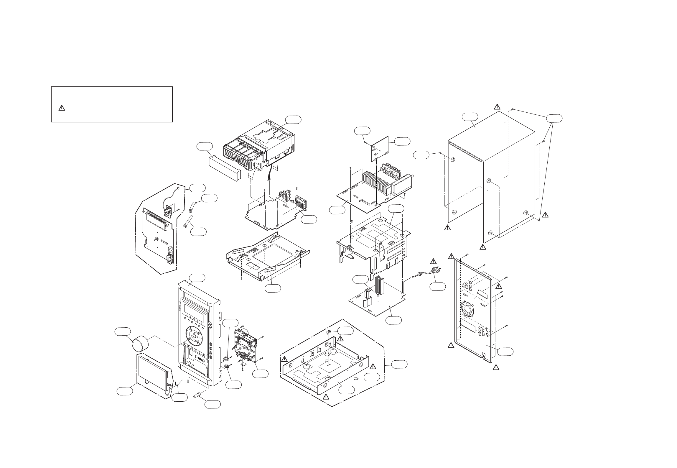
SECTION 2. EXPLODED VIEWS
1. CABINET AND MAIN FRAME SECTION
A26
A51
263
A000
256
255
254
253
251
250
MAC
257
463
262
261
463
463
A48
259
274
A44
273
276
A46
265
264
A50
A47
300
450
SMPS
MAIN
DVD
FRONT
252
2-1 2-2
NOTE) THE EXCLAMATION POINT WITHIN AN
EQUILATERAL TRIANGLE IS INTENDED
TO ALERT THE SERVICE PERSONNEL TO
THE PRESENCE OF IMPORTANT SAFETY
INFORMATION IN SERVICE LITERATURE.
Page 11
2-3 2-4
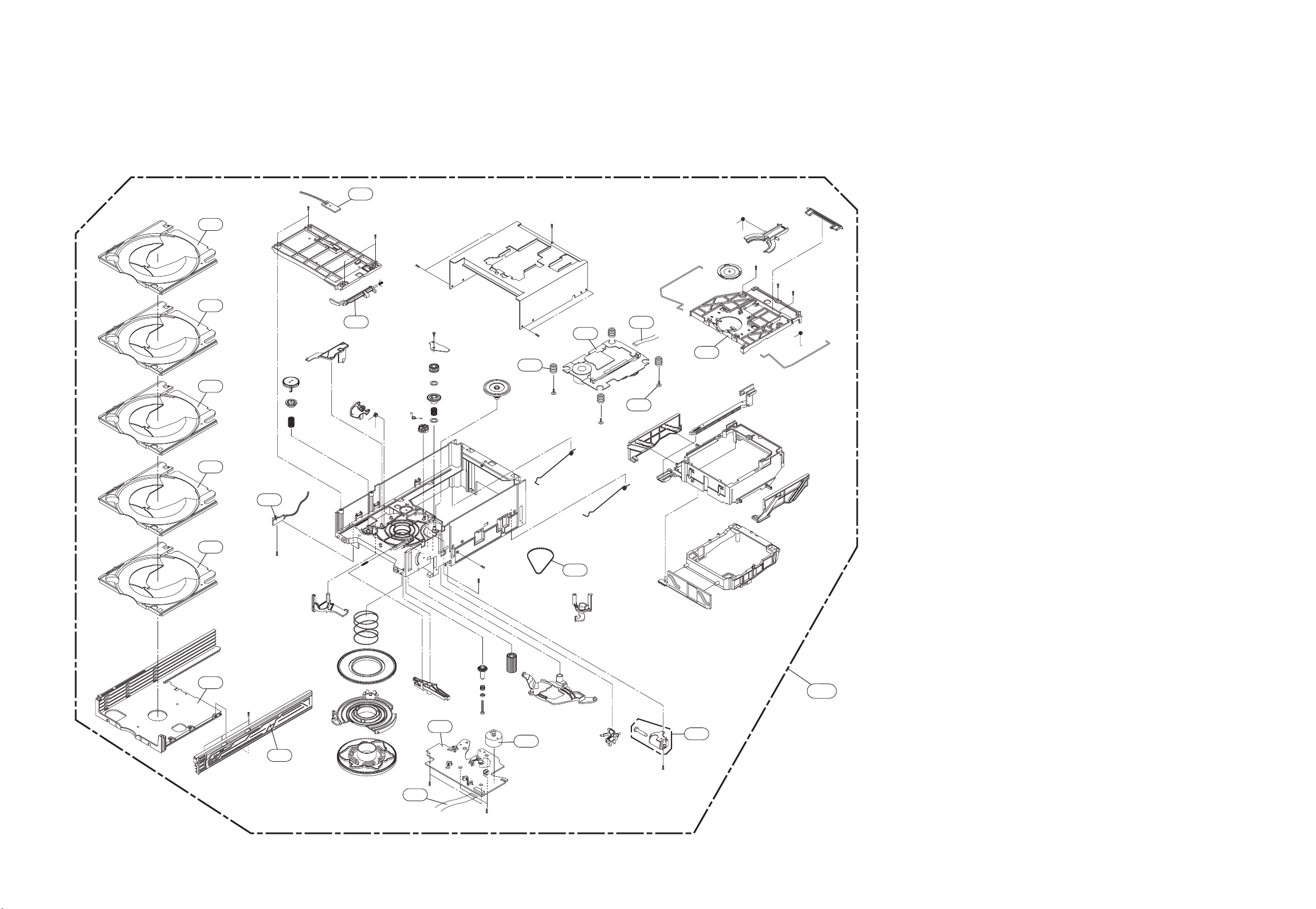
2. DECK MECHANISM EXPLODED VIEW (5 CHANGER)
A26
003
075
023
011
038
073
037
032
062
031
004
005
006
007
001
002
071
431
074
072
Page 12
2-5 2-6
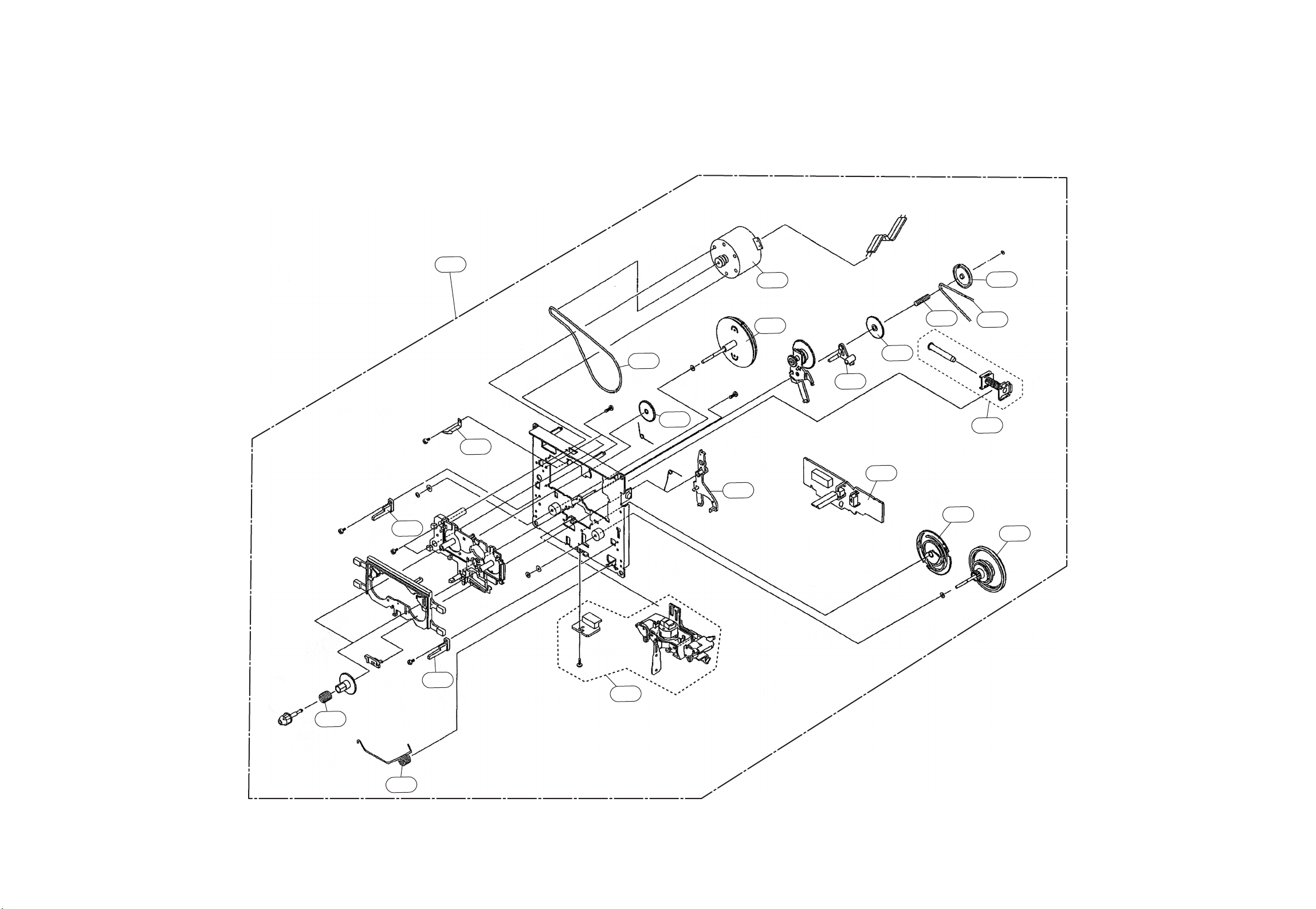
3. TAPE DECK MECHANISM
1011
1013
1009
1009
1003
1002
1007
1037
1006
1018
1017
1019
1020
1021
1022
A001
1023
A000
1025
A002
1015
Page 13
- 2-7 -
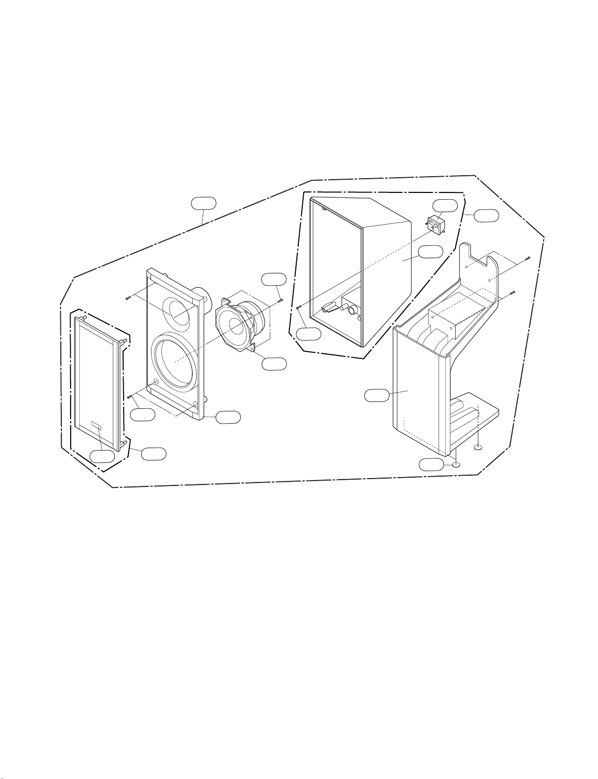
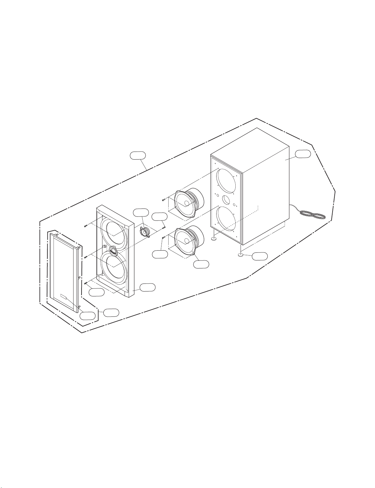
4. SPEAKER EXPLODED VIEW
1) LXS-K7960T/LXS-D6960T
859
860
856
857
858
855
852
854
853
A800
850
852
851
Page 14
- 2-8 -
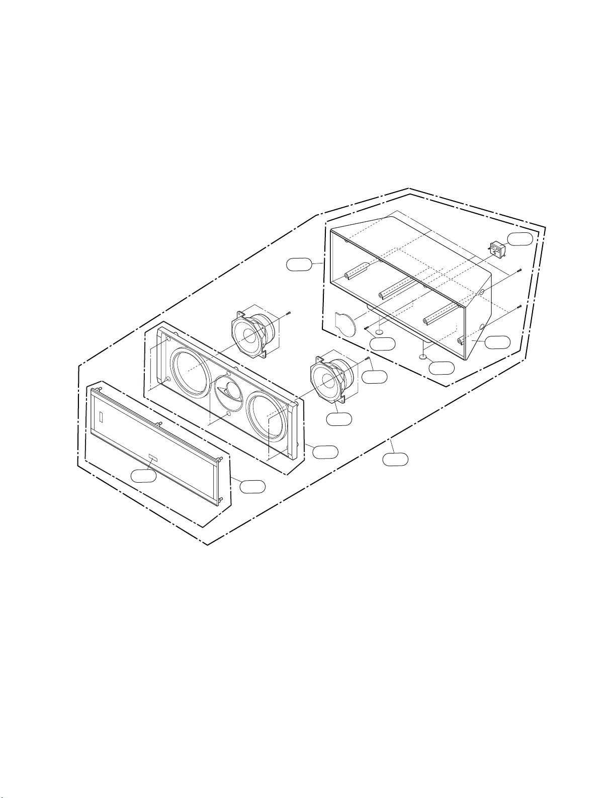
2) LXS-K7960V/D2560V/D2960V/K4960V/D3960V
LFS-K3560V/K3565V/K3960V
758
757
A700
756
754
755
753
752
751
750
759
Page 15
- 2-9 -
3) LXS-K7960C/D6960C
653
A600
652
651
650
654
659
655
658
657
656
Page 16
- 2-10 -
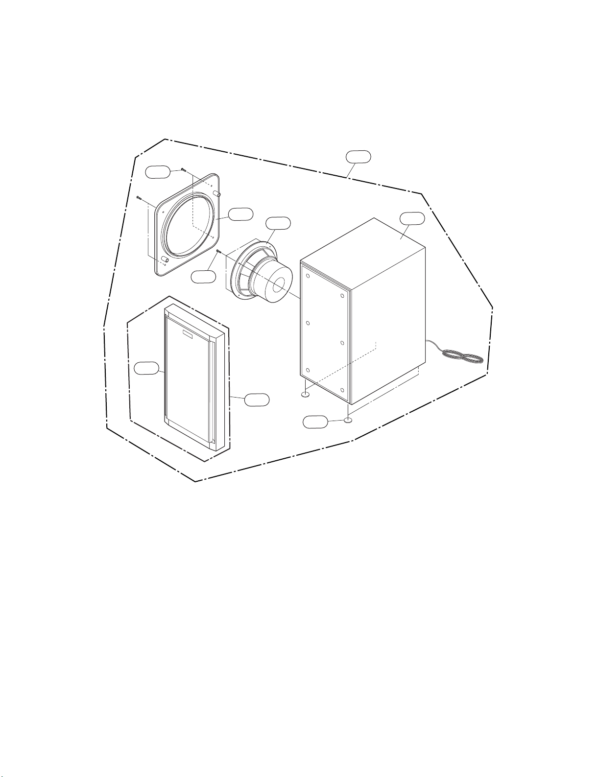
4) LXS-K7960W/K4960W/D6960W/D3960W
955
954
953
952
956
A900
957
950
951
Page 17
- 3-1 -
SECTION 3. ELECTRICAL SECTION
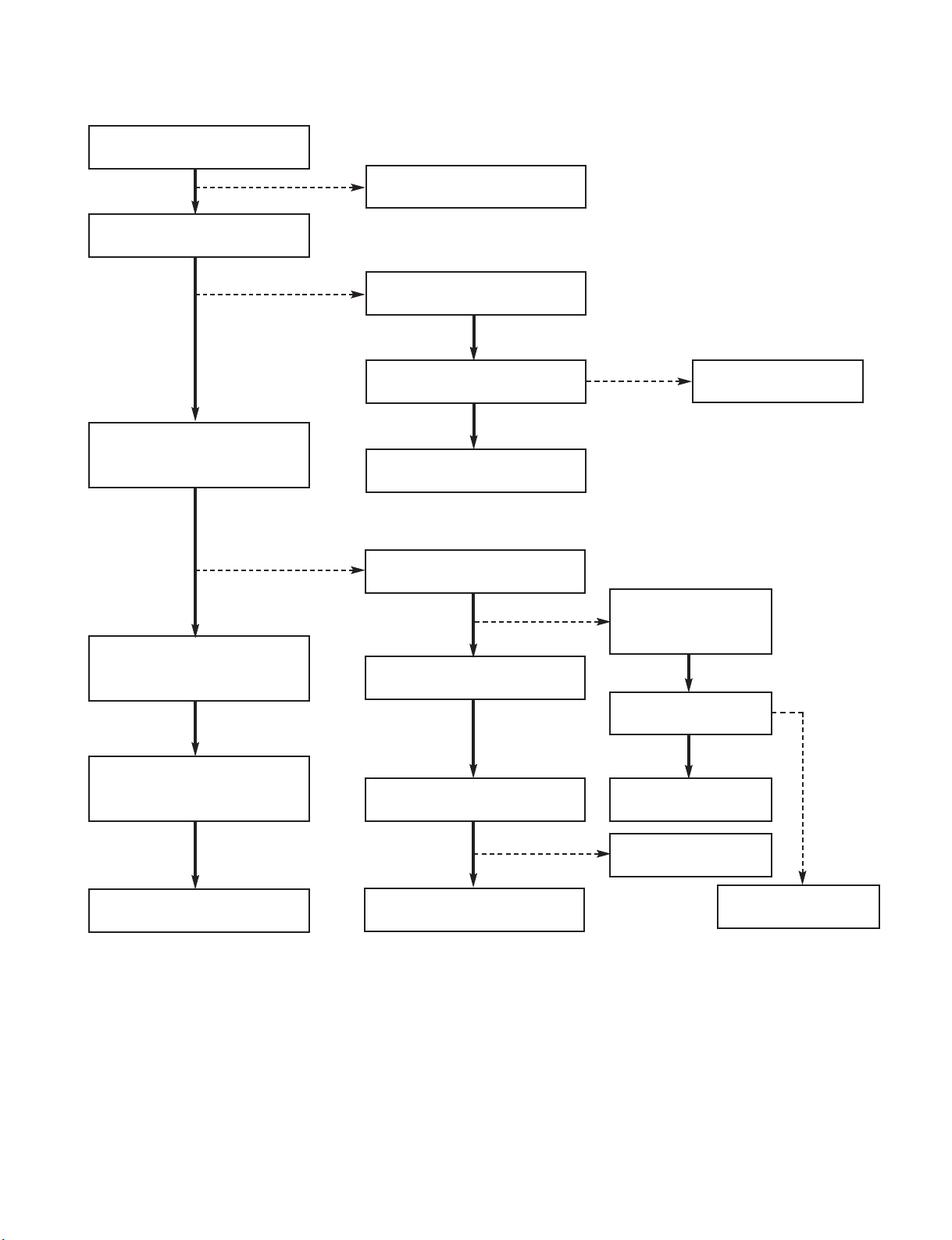
❏ ELECTRICAL TROUBLESHOOTING GUIDE
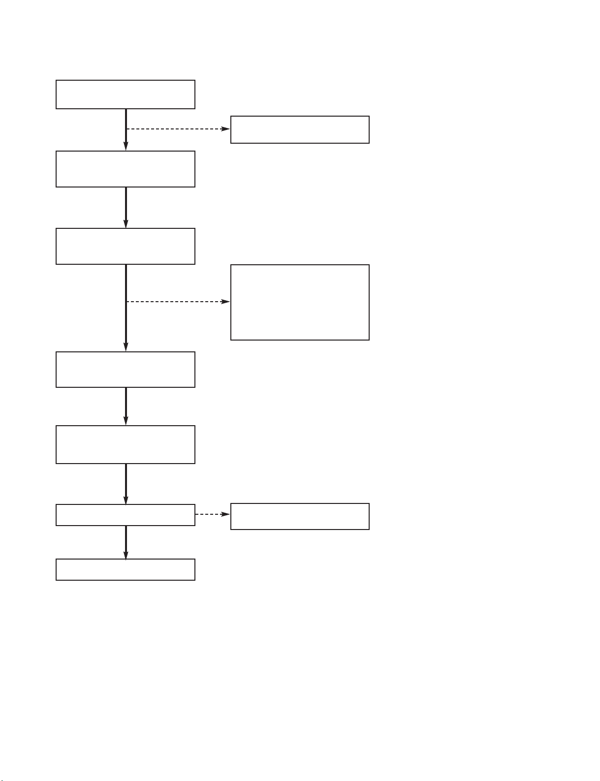
Check P7904 6PIN P-SENS
Refer to SMPS
Troubleshooting
Check if IC101 KIA7042
input is over 5V.
Check if output voltage
of IC101 KIA7042 is 4.3V
Check the related part
of IC101 KIA7042
Replace the
related parts
OK
Check power of both
terminals of IC101 KIA7042
Check IC100 78KO/KF2
1 PIN power
OK
YES
NO
NO
NO NO
YES
YES
YES
YES
■ MICOM PART CHECK I
Page 18
- 3-2 -
Check Q102 BASE
PIN 0.6V HIGH
Check Q102 COLLECTOR
Check output power
of IC101 KIA7042 is
over 4.3V.
Check the related
part.
Replace the
related parts
OK
Replace the
related parts
Check the related part.
OK
Check IC103 8PIN IC100
19,20,59 PIN 5V
Check the working condition
X101: 32.768kHz
X100: 9.8304MHz
OK
Check P7904 5PIN 5.6V
Refer to SMPS
Troubleshooting
Check D101 1SR35
output is working on 5V
Check the related part
OK
Replace the
related parts
Check power of both
terminals of D101 1SR35
Check Q101 EMITTER 5V
and COLLECTOR 5V
NO
NO
NO
NO
NO
YES
YES
YES
YES
YES
YES
YES
YES
YES
YES
YES
YES
■ MICOM PART CHECK II
Page 19
- 3-3 -
Check IC100 78KOKF2
22,24 PIN
22 PIN DATA 22 PIN CLK Check MICOM power 5V
Refer to MICOM
Troubleshooting
Replace the related parts
Check the related part
OK
Refer to SMPS
Troubleshooting
Check P7302 assembly
Check power of each PIN
OK
Replace the related part
OK
Check P7904 1,2,3 power.
F1+,F2- both terminals: over
3.7V Check power VKK: over
26V.
Check P7302 connection
condition and power F1+,F2both terminals: over 3.7V
Check power VKK: over 26V
Check 25 PIN:5.6V
Check IC301 PT6324
power 50 PIN VKK:-26V
9.52 PIN +5V
YES
YES
YES
YES
YES
YES
YES
YES
YES
YES
NO
NO
NO
NO
NO
NO
■ IC103 KS4CD21CS CHECK
■ FLD DISPLAY CHECK
Page 20
- 3-4 -
Check IC100 ➞ IC301 DATA
communication
PIN PIN
75 PIN
➞ 3PIN STB
76 PIN
➞ 2PIN DO
77 PIN
➞ 4PIN DI
78 PIN
➞ 1PIN CLK
When 5V fails,check
D3191SR35 input and
output power
Check the related part
Check 76 PIN ➞ DO
➞ DATA input
Check the related part
Replace the related part
OK
Replace the related part
OK
FLT light on
OK
IC100
75 PIN ➞ STB
77 PIN
➞ 4PIN DI
78 PIN
➞ 1PIN CLK
Check Data output.
YES
YES
YES
YES
YES
YES
YES
YES
NO
NO
NO
NO
Page 21
- 3-5 -
Check P7905 9PIN 3.3V
Check if X601 12.288MHz is
working.
Check IC604 PS9829
86 PIN CLK input
Check output of
IC100 78KOKF2
21
➞ PWM_CLK
22
➞ PWM_DATA
23
➞ PWM_REST
Check IC604 PS9829 DATA
input
78 PIN
➞ DATA
79 PIN
➞ CLK
96 PIN
➞ REST
Check PWM MODULATOR
output
FL:75(+)74(-) FR:71(+)70(-)
SW:68(+)67(-) CEN:62(+)61(-)
SL:59(+)58(-) SR:52(+)51(-)
OK
Check IC604 PS9829 VDD
PIN power (3,10,22,29,39,47,
56,65,72,87,94) Check X601
2PIN 3 3V
Refer to SMPS
Troubleshooting
Check the related part of
X601
OK
Check R668(470Ω) output
OK
Check resistance output of
LINE
DATA: R671
CLK: R670
RST: R665
OK
Check DVD ASS`Y PS9829
communication condition (P7403)
Check IC604 PS9829 DATA input
OK
Check IC604 PS9829 part.
Replace the related
part
Replace the related
part
Replace the related
part
Refer to DVD
Troubleshooting
Check resistance
output of each LINE
YES
YES
YES
YES
YES
YES
YES
YES
YES
YES
YES
YES
NO
NO
NO
NO
NO
NO
NO
NO
NO
NO
NO
■ PWM MODULATION PART
Page 22
- 3-6 -
P7905 3 PIN+12 13,14,15
PIN 32V
Check input power of
eachIC700,701,702,703
34,29,26,21 PIN.
Check input power of each
IC 700,701,702,703
1,36,17,18,19 PIN +12V
Check PWM MODULATOR
input of each IC 4,6,14,16
PIN
Check POWER IC 700,701,
702,703 34,29,27,20 PIN
output.
Check output LINE COIL
OK
Refer to SMPS
Troubleshooting
Check resistance power of
each LINE
IC700:R702,701,726,727,724
IC701:R730,729,750,753,752
IC702:R756,755,768,771,770
IC703:R774,773,794,797,796
Replace the related parts
YES
YES
YES
YES
YES
YES
NO
NO
NO
■ POWER AMP PART CHECK
Page 23
- 3-7 -
Check if JK800 contacts with
Check IC200 (BU4052)
4, 11PIN input waveform.
Check IC200 (BU4052)
3, 13PIN output waveform.
Check IC801 (MC4580)
2, 6PIN input waveform.
OK
Check IC200 (BU4052)
16PIN VDD, 8PIN VSS power.
Check u-COM (IC301)
83PIN, 84PIN
communication.
Refer to SMPS
Troubleshooting.
Replace the related parts
Check IC801 (MC4580)4PIN
VSS, 8PIN VDD power.
Replace the related parts.
YES
YES
YES
YES
YES
YES
NO
NO
NO
NO
■ AUX FUNCTION
Page 24
- 3-8 -
Check TUNER
module(TU601) is working.
Check TUNER MODUEL
power(Check 2PIN 9V)
Check IC200(BU4052)
16PIN VDD,8PIN VSS power
Replace the related parts
Replace the related parts
Check IC200 (BU4052)
16PINVDD,8PIN VSS power.
Replace the related parts
IC200(BU4052) 16PINVDD,8PIN VSS power check
Replace the related parts
Check IC801(MC4580) 4PIN
VSS,8PIN VDD power
Check IC200(BU4052)
1, 12PIN input waveform.
Check IC200(BU4052)
3,13PIN output waveform.
Check IC601(BU 4502)
2, 15PIN Check 25 PIN:5.6V
Check IC801(MC4580)
2,6PIN input waveform.
OK
TAPE PCB ASS`Y
Check IC801 (MC4580)
2,6PIN input waveform.
OK
Check IC200(BU4052)2,1
5PIN input waveform.
Check IC200 (BU4052)
3,13PIN output waveform.
Check IC601 (BU4052)
2,15PIN input waveform.
YES
YES
YES
YES
YES
YES
YES
YES
YES
YES
YES
YES
NO
NO
NO
NO
NO
■ TUNER FUNCTION CHECK
■ TAPE FUNCTION CHECK
Page 25
- 3-9 -
P2707:4 PIN ➞ 12V
Check IC201 (HA12237)16
PIN 12V input.
Check IC201: 5.26 PIN
Signal Output.
Check IC201 14 PIN MUTE
is working.
OK
Refer to SMPS
Troubleshooting
Check DECK HEAD input.
Check DECK HEAD input
IC201 32.39 PIN.
Replace the HEAD
WIRE and Mecha.
Replace the
related parts.
Replace the
related parts.
Check the related part.
OK
Check IC202 10 PIN HIGH is
working.
Check the related part.
OK
YES
YES
YES
YES
YES
YES
YES
YES
YES
NO
NO
NO
NO
NO
NO
■ TAPE PLAY PART CHECK
Page 26

- 3-10 -
Check IC604 PS9829
#49,#52 PWM output.
Refer to PWM modulation
part.
Check Q601 Collector waveform.
Check Board to Board contact.
Check IC203 8 PIN +12V.
Check the related part.
OK
Check Q205(D1304)
BASE HIGH.
Check IC202 4 PIN HIGH
working.
Refer to SMPS
Troubleshooting
Replace the related parts
Replace the related parts
OK
Check P7207 #2,#4 output.
Check P2707 #5,#7 input.
Check IC203 MC4580 #1,#7.
Check IC201 10,21 PIN
output.
Check L203 2,3 PIN oscillation.
Check .P2203 5,3 PIN input.
Check .8 PIN ERASE input.
OK
YES
YES
YES
YES
YES
YES
YES
YES
YES
YES
YES
NO
NO
NO
NO
NO
NO
NO
NO
■ TAPE REC PART CHECK
Page 27

- 3-11 -
Check the fuse F901
Check the DC V of C905.
If DC V is over 400V
Check the DC V Of
C981,C945. If DC V is 6.1V
OK
Chcek the DC V Of
C950,C951 If DC V is in
35V,-35V
Chcek the DC V Of
C909,C903,C921 If DC V is
in 14~19V and it is steady.
Replace the fuse
Check BD901,LF901,902
Check IC901,902 Replace IC 901,902
Check short of P9702 line
Check short of P9701 line
Check short of P9701,
P9702 line
*MAIN PART
YES
NO
YES
YES
YES
YES
YES
NO
NO NO
NO
NO
■ SMPS POWER CIRCUIT
Page 28

- 3-12 -
Check the PIN6 OF P9702
If DC V is over5.6V
OK
Check power circuit
Trouble shooting
*P-SENS PART
Check the PIN3 OF P9702
If DC V is over -28V ±2
OK
Check power circuit
Trouble shooting
*VKK PART
YES
YES
NO
NO
Page 29

- 3-13 -
❏ INTERNAL BLOCK DIAGRAM of ICs
• UTC MC4580
PIN CONFIGURATION
TEST CIRCUIT
Page 30

- 3-14 -
• NJM 2279
BLOCK DIAGRAM
6dB 75Ω
6dB 75Ω
Vout1
Vout2
Driver
Driver
V+MUTE1SW2
20kΩ
Vin1
Vin2
Vin3
SW1 MUTE2 GND1 GND2 V-
20kΩ
20kΩ
20kΩ
20kΩ
4.14kΩ
4.14kΩ
4.45kΩ
4.45kΩ
AMP.
AMP.
• MBM29LV160TE
BLOCK DIAGRAM
Page 31

- 3-15 -
• HY57V281620ETP
FUNCTIONAL BLOCK DIAGRAM
• FAN8082D
Internal Block Diagram
Page 32

- 3-16 -
• BU2090
Block diagram
Page 33

- 3-17 -
• HA12237F
BLOCK DIAGRAM
Page 34

- 3-18 -
• BA3308 / BA3308F
BLOCK DIAGRAM
BA3308
BA3308F
Page 35

- 3-19 -
• TAS5142
BLOCK DIAGRAM
Page 36

- 3-20 -
• HT1200-4
SYSTEM BLOCK DIAGRAM
Page 37

- 3-21 -
• HT1200-4
FUNCTIONAL BLOCK DIAGRAM
Page 38

- 3-22 -
• CS5340
BLOCK DIAGRAM
• BU4052
BLOCK DIAGRAM
Page 39

- 3-23 -
• STR-S6757IF1905
BLOCK DIAGRAM
• STR-A6200
BLOCK DIAGRAM
Page 40

- 3-24 -
Page 41

3-25 3-26
❏ WIRING DIAGRAM
Page 42

3-27 3-28
❏ BLOCK DIAGRAM
OVERALL AV BLOCK
DIAGRAM
LC6324
REC L/R
12.288 TAS5152_SD
FL+/-, FR+/-
9829_RESET
9829_CLK
LEVEL METER
9829_DAT
MAIN BOARD AMP BOARD9.8304MHz
VFD DATA.CLK
EXP CLK
DATA
RL+/-, RR+/CENTER +/WOOFER+/-
TAS5152_PDN
CS5340
CLK.DATA
OP AMP
SUB WOOFER
HEAD WOOFER
DVD DATA.CLK
OPTICAL
USB DA+,-,5V
OP AMP
EXPENDER
DECK
HA12237
TAPE IC
BU4052
OP AMP
CS5340
TUNER
MODULE
NEC
AUDIO
MICOM
PS9829A
PWM
MODUL
ATOR
TAS5142
Power Amp
H/P_SW
PWM OUT
DVD/CD
BLOCK
DECK/AD
MODE A.B
SOL"A"
RM
OP AMP
RDS
DATA CLK
PLL DAT.CLK
BU4052 DATA CS5340 RESET
DVD DATA CLK
12.28MHz
TUNER L/R
TAPE L/R
AUX L/RAUX L/R
MIC INPUT
SOL"B"
MOTER
HIGH/NO
HALF A.B
REC F.R
REC MUTE
REC MUTE
REC RETM
REC SW
REC MUTE
FL
FR
S/W
C/T
RL
RR
Page 43

3-29 3-30
❏ SCHEMATIC DIAGRAMS
• MAIN SCHEMATIC DIAGRAM
MIC
A_MUTE
UART
12S
12S
Y
Y
Y/G
MIC L, R
AUDIO L, R
CYBS,C,pb,pr,R,B
SCI
SDA
MMA[0..1MB]B[0..15]
SPDIF OUT
SPDIF IN
A,B,C,D,E,F,R
CDMDI, DVDMDI
CDDVDCT, VRDVD,VRD
LDO1,LDO2
OPEN/CLOSE
SLED±, F±,T±
48MHz
27MHz
LOAD±,SPINDLE±
USB_RESET
D-, D+
HD[0..15], CONTROL SIGNAL
MCU_INTQ
JRD#,HWR#
MS_SEL_OU
HA0
HD[0..7]
FOCUS/SLED
SPINDLE/TACKING
AMP_STBY
DSCK#,CKE,CSo#,RAS0
CAS#,WE#,DQMX
LA[0..21], LD[0..7]
WRLL#,MRST#,LOE#
AUDIO
JACK
VIDIO
OUT
P/UP
M
DECK MECHANISM
MOTOR
DRIVE
IC
USB
CON
USB
UBI9021
SWITCH
OPT
IN
OPT
OUT
ADC
PWM/DAC
MICOM
SDRAM
MPEG
ESS6838
FLASH
EEPROM
Page 44

3-31 3-32
• µ-COM/INTERFACE/PWM SCHEMATIC DIAGRAM
Page 45

3-33 3-34
• 6CH_AMP SCHEMATIC DIAGRAM
Page 46

3-35 3-36
• FRONT SCHEMATIC DIAGRAM
Page 47

3-37 3-38
• SMPS SCHEMATIC DIAGRAM
Page 48

3-39 3-40
• DECK SCHEMATIC DIAGRAM
Page 49

3-41 3-42
❏ PRINTED CIRCUIT DIAGRAMS
• MAIN P.C. BOARD
Page 50

3-43 3-44
• MAIN P.C. BOARD
Page 51

3-45 3-46
• FRONT P.C. BOARD
Page 52

3-47 3-48
• SMPS P.C. BOARD
Page 53

3-49 3-50
• DECK P.C. BOARD
Page 54

Page 55

- 4-1 -
SECTION 4. DVD PART ELECTRICAL
❏ DVD ELECTRICAL TROUBLESHOOTIHG GUIDE
■ POWER CHECK GUIDE
Power ON Power ON
Does DVD/CD
appear at FLD?
Does DISK1
appear at FLD?
Check the
voltage of each pin on
P5701.
Check DVD MD Module.
Check connector P7501.
Reconnect it.
OK.
Does AUX, FM 87.5
appear at FLD?
Does it
appear DVD ERROR at
FLD?
PUSH KARAOKE
DVD BUTTON
Check
Connector (P4405,P4407,
P4408).
Check an Audio Micom
or interface reconnect (P4703)
OK
Does No DISC or
Time are appeared at
FLD?
NO
NO
NO
NO
NO
YES
YES
YES
YES
YES
Page 56

- 4-2 -
B
POWER ON
Show LOGO?
Flash
Memory operates
properly?
SDRAM works
properly?
Check AV cable
connection to TV set.
SW5 &SW7 signals
on P4408 are OK?
Check the MD mecha
Check the related circuit of
ES6698FD (IC501)PIN
133,134,137,138,139,140
Check connection lines between
SDRAM (IC502)&ES8381 or the
SDRAM is damaged.
CHECK THE OUTPUT SIGNAL
OF ES8381 TO IC401 FOR
CONTROL OPEN/CLOSE
Check the Tray control
I/O Pin on IC401.
OPEN /CLOSE
signals on IC401 are
OK?
Load+&load-
signals on P4408
are OK?
Check the cable
connection between DVD
PCB and MD (MECHA)
Does first
tray move inside when
it is at closed
position?
ES8381 VIDEO
outputs
properly?
Check connection lines between
FLASH &ES8381 or the FLASH access
time whether is suitable or not.
■ TEST & DEBUG FLOW
YES
YES
YES
YES
YES
YES
YES
YES
YES
NO
NO
NO
NO
NONO
NO
NO
Page 57

- 4-3 -
Does
the SLED move to
inner side when it is at
outer position?
Limit SW signal
on P4407 is LOW?
SLED signal is OK?
Check the cable
connection with MECHA.
Proper Focus
outputs to motor
driver?
Proper F+&F-
outputs?
Check the motor driver (IC401).
Check Focus connection on ES8381
and motor driver IC.
Check the related circuit of SLED
and Motor driver IC (IC401)
Check the MD
Check cable connection
with pick-up head.
Do not put in disc and
tray close.
Optical Lens
is moving for searching
Focus?
B
C
YES
YES
YES
YES
YES
YES
YES
NO
NONO
NO NO
NO
Page 58

- 4-4 -
C
Laser turns
on when reading
disc?
DVDLD or CDLD
output properly?
Check cable connection
between P4405 and
pick-up head.
Proper SPINDLE
signal on ES8381.
SPIN+&SPIN-
output properly?
Check the cable
connection between
P4407 and MD
Check the SPINDLE control of motor driver
(IC404).
Check the SPINDLE related
circuit on ES8381
Check the related circuit of laser
power transistor.
Check the laser power circuit between
ES8381 and power
transistor. (Q405,Q406)
Collector
voltage of power
transistor is ok?
(Q405,Q406)
Put disc in tray.
Does SPINDLE
rotate?
D
YES
YES
YES
YES
YES
YES
YES
NO NO
NO
NO
NO
NO
Page 59

- 4-5 -
D
E
Focus On OK?
Proper signal on
A,B,C,D from MD?
Check the connections between
P4405 and pick-up head.
Check the related circuit of ES8381
FOCUS signal.
Check the related circuit between
IC401 and ES8381
Check the Tracking control
on motor driver (IC401).
Proper FOO signal
on IC401?
Check cable connection
between P4405 and MD.
Proper TRO signal
on IC401?
T+&T-output
properly?
Check cable connection
on pick-up head.
Check RF signal waveform.
Track On OK?
Disc play?
YES
YES
YES
YES
YES
YES
NO NO
NO
NO
NO
NO
NO
Page 60

- 4-6 -
E
All outputs
are Ok during playing
DISK ?
TEST END
Audio signal
data on P4703 is OK?
Check the MAIN PCB
Picture
signal data on ES8381
is OK?
For example composite video ,
Check the video mute TR (Q411),
Output of Video buffer IC (IC407)and
ES8381 video signal data
Check the connections between
ES8381 and P4703
NO
NO NO
NO
YES
YES
Page 61

- 4-7 -
■ USB PART
TURN ON USB
“Searching ”or
“USB ”Display
check
Reading OK check
OK
Check the POWER supply circuit.
(Check P5701)
Check the HRST#signal
Check the USB PART
and DVD PART line.
Check the USB JACK POWER supply.
(Check P4302)
Check the USB DATA LINE.(P4302)
Check the IC405 (UBI9021).
(Check DATA LINE PIN 14~17,20~23)
NO
NO
YES
YES
YES
YES
YES
YES
YES
Page 62

- 4-8 -
WHEN POWER ON,RESET &DATA ETC WAVEFORM
1.RESET(DVD)
2.RX
3.TX
4.LCS3#(FLASH)
Playing at USB
function
1.HRST#
2.5V
3.D-
4.D+
Page 63

- 4-9 -
OPEN/CLOSE WAVEFORM AT POWER ON
STARTING ACTION WAVEFORM IN MD DEVICE
1.Limit SW
2.OPEN
3.CLOSE
1.SLO (from
MPEG)
2.SLED-
3.SLED+
(At Power on )
Page 64

- 4-10 -
FOCUS WAVEFORM (AT CD)
FOCUS WAVEFORM (AT DVD)
1.FDO
2.F+
3.F-
(INSERT CD )
(INSERT DVD )
1.FDO
2.F+
3.F-
Page 65

- 4-11 -
1.Spind
2.Spin+
3.Spin-
1.A
2.B
3.C
4.D
AT POWER ON ,SPINDLE SIGNAL AT MD DECK
AT FIRST ACTION,FOCUS SIGNAL A,B,C,D
Page 66

- 4-12 -
TRACKING SIGNAL
RF WAVEFORM
1.Tro
2.Tr-
3.Tr+
Page 67

- 4-13 -
DISK TYPE JUGEMENT WAVEFORM
1.F+
2.FDO
3.SVRRF
(DVD)
(CD)
Page 68

- 4-14 -
Page 69

4-15 4-16
❏ DVD SCHEMATIC DIAGRAMS
• MPEG SCHEMATIC DIAGRAM
Page 70

4-17 4-18
• RF & SERVO SCHEMATIC DIAGRAM
Page 71

4-19 4-20
• AV SCHEMATIC DIAGRAM
Page 72

4-21 4-22
• USB/PC-LINK SCHEMATIC DIAGRAM
Page 73

4-23 4-24
❏ DVD PRINTED CIRCUIT DIAGRAMS
• DVD MAIN P.C. BOARD
Page 74

4-25 4-26
• DVD MAIN P.C. BOARD
Page 75

5-1
SECTION 5 MECHANISM OF DVD PART (5 CHANGER)
1. Disassembling of Traverse Ass’y
2. Disassembling of Cover S
1) Release 4 Screws.
2) Lift up the Traverse Ass’y from the
Mechanism Ass’y. In case of not coming out
easily to stuck to a both sides, pull Spring in
direction of left/right side and lift it up.
1) Release 5 Screws 2) Seperate 2 Stoppers connected to Cover S
and Clamp Ass’y from the Cover S.
In case of not seperating easily, use a gimlet or a screwdriver to seperate it as shown
in the picture.
3) Widen a both sides of Cover S(caution of
permanent transformation) and lift it up
from the Ass’y.
Damper
(4900RB0005A)
Traverse Ass’y
(6717R-D001B)
Mechanism Ass’y
(4404R-D001B)
Cover S
Stopper
❏
DECK MECHANISM DISASSEMBLY
Page 76

5-2
WH
BL
SW8
BL
4.
Disassembling of Frame LG Ass’y
3. Disassembling of Clamp Ass’y
3
1
2
1) Release 4 Screws attached in Frame LG
Ass’y
2) Release the Wire of PWB PH Ass’y
soldered on the back side PCB Ass’y of
Mechanism Ass’y, and then lift up the
Frame LG.
1) Turn the Gear Cam to counterclockwise and
then down the Clamp Ass’y as shown in the
picture.
2) Release 3 Screws attached in the Clamp
Ass’y.
3) Lift up the Clamp Ass’y and seperate it.
Clamp Ass’y
(4260RZ0004A)
Gear Cam
Frame LG Ass’y
PWB PH Ass’y Wire
PCB Ass’y
(6871RZ0045A)
Page 77

5-3
1
2
1
5. Disassembling of PWB PH Ass’y
7.
Disassembling of Drawer Ass’y
6. Disassembling of Arm SW C
1) Unlock the two parts of Locking Tab on the
Frame LG and seperate.
1) Unlock the Frame LG locking Tab and lift it
up as shown in the picture.
1) Turn the Gear Cam to counterclockwise
and then lift up the FL Base to the top.
2) Pull front the Drawer Ass’y, and push the
left/right side of Chassis at the end and
then seperate the Drawer Ass’y.
PWB PH Ass’y
(6871RZ0045B)
Locking Tab
FL Base
Chassis
Drawer Ass’y
Gear Cam
Locking Tab
Spring C
Arm SW C
(4260RZ0001C)
Page 78

5-4
WH
BL
SW8
BL
10. Disassembling of PCB Ass’y
8. Disassembling of Carriage 9. Disassembling of Belt
1) Extract 5 Carriages in the direction of arrow
from the Drawer.
1) After seperating of the Drawer, remove the
Belt from the top of the Chassis.
1) Release the Screws (big 2/small2) that
connects between the Chassis and the
PCB Ass’y and then seperate the PCB
Ass’y from the Chassis.
2) At this moment, remove the solder,
because the Wire of PCB SW Ass’y is
soldered on PCB Ass’y.
Drawer L
(3210RZH001A)
Drawer R
(3210RZH002A)
Carriage
(3390RZ0002A~E)
PCB Ass’y
(6871RZ0022A)
PCB Ass’y
(6871RZ0022A)
Belt
(4400RZ0002A)
Page 79

5-5
SOL
MM+
MM-
11. Disassembling of Motor
12. Disassembling of Solenoid Ass’y
3) Release the Screw which fixes the Switch to
the Chassis and then seperate the PCB SW
Ass’y.
4) Remove the solder on the Motor and the
PCB Ass’y.
5) Lift up the PCB Ass’y.
1) Release the 2 Screws which fixes the
Chassis and the Motor, and then se
perate it.
1) Release the 2 Screws which fixes the
Bracket of Solenoid Ass’y, and then
seperate the Solenoid.
PCB Ass’y
(6871RZ0045C)
Motor
(4681RZ0001A)
Solenoid Ass’y
(6768RZVP01A)
Page 80

5-6
Page 81

5-7 5-8
❏ EXPLODED VIEW
• DECK MECHANISM EXPLODED VIEW
A26
003
075
023
011
038
073
032
062
031
004
005
006
007
001
002
071
431
074
072
037
Page 82

 Loading...