

Page 1
PanelMatch™ StayLit™ LXMG1626-12-45
TM
The LXMG1626-12-45 is a Dual 6W
Output Direct Drive™ CCFL (Cold
Cathode Fluorescent Lamp) Inverter
Module specifically designed to be
compatible with variety of LCD panels
DESCRIPTION
lamps in the LCD fails open, the second
lamp will continue to operate with a
FAULT signal toggling to indicate the
failed condition, StayLit™ feature.
that have both lamps on one side of the
panel and use a single common lamp
return wire.
LXMG1626 modules provide the
Technique provides flicker-free brightness
control in any wide range (typically
100:1+) dimming application.
designer with a superior display brightness
range. This brightness range is achievable
with virtually any LCD display.
The modules are available with a
dimming input that permits brightness
control from either, a DC voltage source,
energizes the lamp is designed
specifically to ensure that no premature
lamp degradation occurs, while allowing
significant power savings at lower dim
levels.
a PWM signal or external potentiometer.
The maximum output current is
externally programmable (through the
input connector) at either 10mA or 12mA
(5mA or 6mA per lamp). This allows the
inverter to match the panel’s lamp current
specifications, or it can be used to
highly integrated LX1691B backlight
controller to convert DC voltage from the
system battery or AC adapter directly to
high frequency, high-voltage waves
required to ignite and operate CCFL
lamps.
purposely drive the lamps at a lower or
higher current to decrease or increase
nominal brightness. The inverter also has
a dedicated FAULT pin that indicates an
open/shorted lamp condition.
IMPORTANT: For the most current data, consult MICROSEMI’s website: http://www.microsemi.com
Protected By U.S. Patents: 5,923,129; 5,930,121; 6,198,234; Patents Pending
are stable fixed-frequency operation,
secondary-side strike-voltage regulation
and both open/shorted lamp protection
with fault timeout.
®
In addition when only one of the two
The RangeMAX™ Digital Dimming
The resultant “burst drive” that
The design utilizes Microsemi’s
Other benefits of this new topology
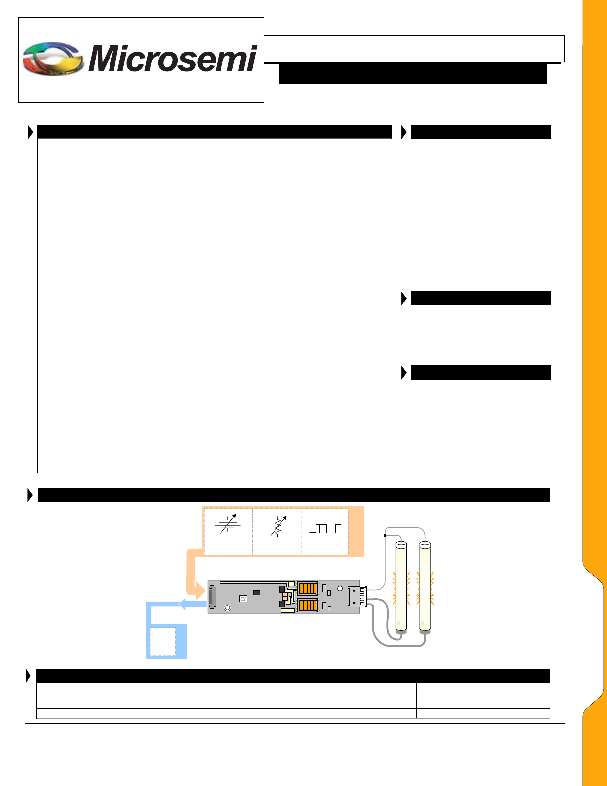
PRODUCT HIGHLIGHT
12V Dual 6W CCFL Programmable Inverter Module
PRODUCTION DATAS HE E T
KEY FEATURES
Externally Programmable
Maximum Output Current
Easy to Use Brightness Control
RangeMAX™ Wide Range
Dimming
Output Open & Short-Circuit
Protection and Automatic StrikeVoltage Regulation and Timeout
StayLit™ Continued Operation
with Single Open Lamp Failure
Fixed Frequency Operation
Fault Output Signal
Rated From -30°C to 80°C
RoHS Compliant
UL60950 E175910
APPLICATIONS
Dual Lamp LCD’s Requiring a
Shared Common Lamp Return
Mates to a Single JST BHR-04
VS-1 Lamp Connector
Industrial Display Controls
BENEFITS
Smooth, Flicker Free 1% - 100%
Full-Range Brightness Control
Programmable Output Current
Allows Inverter to Mate With a
Wide Variety of LCD Panel’s
Specifications
Output Open Circuit Voltage
Regulation Minimizes Corona
Discharge For High Reliability
WWW.Microsemi .COM
DC Voltage
Source
Potentiometer
Microsemi
UNIVERSAL DIMMING INPUT
Lamp
Fault
Signal
OUTPUT
PART NUMBER OUTPUT CONNECTOR
LXMG1626-12-45 JST SM04(4.0)B-BHS-1-TB(LF)(SN), Yeon Ho 20015WR-07A00 or equivalent JST BHR-04VS-1
Copyright © 2007
Rev.1.1, 2007-08-24
11861 Western Avenue, Garden Grove, CA. 92841, 714-898-8121, Fax: 714-893-2570
"PWM", VDC, OR POTENTIOMETER
Lamp current 5 or 6mA per Lamp
PACKAGE ORDER INFO
Microsemi
Analog Mixed Signal Group
PWM
Signal
INPUT
4
123
W
HI
HI
I
NVERTER MATES DIRECTLY
TO
PANEL CONNECTORS
Page 1
L
L
X
X
M
M
G
G
1
1
6
6
2
2
6
6
-
-
1
1
2
2
-
-
4
4
5
5
Page 2
PanelMatch™ StayLit™ LXMG1626-12-45
TM
®
12V Dual 6W CCFL Programmable Inverter Module
PRODUCTION DATAS HE E T
Input Signal Voltage (VIN) ......................................................................................................................................-0.3V to 15V
Input Power......................................................................................................................................................................... 8W
Output Voltage, no load ............................................................................................................ Internally Limited to 1500V
Output Current (per lamp) ...........................................................................................................6.6mA
Output Power ..................................................................................................................................................................... 6W
Input Signal Voltage (
SLEEP
Input)..................................................................................................................-0.3V to 13.2V
Input Signal Voltage (BRITE) ...............................................................................................................................-0.3V to 5.5V
Ambient Operating Temperature, zero airflow.....................................................................................................-30°C to 80°C
Operating Relative Humidity, non-condensing ................................................................................................................ ≤90%
Storage Temperature Range...............................................................................................................................-40°C to 85°C
Exceeding these ratings could cause damage to the device. All voltages are with respect to Ground. Currents are positive into, negative out of specified
terminal.
RECOMMENDED OPERATING CONDITIONS (R.C.)
This module has been designed to operate over a wide range of input and output conditions. However, best efficiency and performance
will be obtained if the module is operated under the condition listed in the ‘R.C.’ column. Min. and Max. columns indicate values beyond
which the inverter, although operational, will not function optimally.
Parameter Symbol
Input Supply Voltage Range (Fully Regulated Lamp
Current)
Input Supply Voltage Range (Functional)
Output Power P
Linear BRITE Control Input Voltage Range V
Lamp Operating Voltage V
Lamp Current (Full Brightness, per Lamp) I
Operating Ambient Temperature Range T
¹ Based on single lamp voltage measurement, use of lamps outside of this range may result is false triggering of the fault detection circuitry.
²At input voltages below 12V the inverter may not be able to output the full 6mA
Unless otherwise specified, the following specifications apply over the recommended operating condition and ambient temperature of
0°C to 60°C except where otherwise noted.
Parameter Symbol Test Conditions
OUTPUT PIN CHARACTERISTICS
`
Full Bright Lamp Current (two lamps) I
Full Bright Lamp Current (two lamps) I
Output Current Lamp to Lamp
Deviation
Min. Average Lamp Current I
Lamp Start Voltage VLS VIN > 10.8V 1250 1400 V
Operating Frequency fO
Burst Frequency f
FAULT Output Voltage High FAULTVH FAULT = -10uA 3 3.5 V
FAULT Output Voltage Low FAULTVL FAULT = 10uA 0.3 0.8 V
ABSOLUTE MAXIMUM RATINGS
(Internally Limited)
RMS
Recommended Operating Conditions
Min R.C. Max
V
IN
4.5 5.5 W
O
0 2.0 V
BRT_ADJ
385 435 485 V
LAMP
5.0 6.0 mA
O(LAMP)
-30 80 °C
A
RMS
10.8 12 13.2
10.2 12 13.6
per lamp in all configurations.
ELECTRICAL CHARACTERISTICS
LXMG1626-12-45
Min Typ Max
L(MAX)
L(MAX)
I
LL%DEV
L(MIN)
BURST
I
= Ground
SET
> 2.0V,
V
BRT_ADJ
I
= Open
SET
> 2.0V,
V
BRT_ADJ
I
= Open
SET
= 0V,
V
BRT_ADJ
I
= Ground; I
SET
V
BRT_ADJ
Output Burst Frequency 215 225 235 Hz
SLEEP
= 2.0V,
> 2.0V,
V
BRT_ADJ
SLEEP
SLEEP
SLEEP
OUT
SLEEP
> 2.0V, V
> 2.0V, V
> 2.0V, V
> 2.0V, V
= I
* SQRT of % duty cycle
MAX
> 2.0V, V
IN
IN
IN
IN
= 12V
IN
= 12V
= 12V
= 12V
= 12V
9 10 11 mA
11 12 13 mA
5 %
1.6 mA
55.2 57.6 60 kHz
Units
V
RMS
RMS
RMS
¹
²
Units
RMS
RMS
RMS
RMS
WWW.Microsemi .COM
E
E
L
L
E
E
C
C
T
T
R
R
I
I
C
C
A
A
L
L
S
S
Copyright © 2007
Rev.1.1, 2007-08-24
Microsemi
Analog Mixed Signal Group
11861 Western Avenue, Garden Grove, CA. 92841, 714-898-8121, Fax: 714-893-2570
Page 2
Page 3

PanelMatch™ StayLit™ LXMG1626-12-45
TM
®
12V Dual 6W CCFL Programmable Inverter Module
PRODUCTION DATAS HE E T
Unless otherwise specified, the following specifications apply over the recommended operating condition and ambient temperature of
0°C to 60°C except where otherwise noted.
Parameter Symbol Test Conditions
BRITE INPUT
`
Input Current I
Minimum Input for Max. Lamp Current V
Maximum Input for Min. Lamp Current V
SLEEP BAR INPUT
`
RUN Mode
SLEEP Mode
SET INPUT
`
SET Low Threshold
Input Current I
POWER CHARACTERISTICS
`
Sleep Current I
Run Current I
Efficiency
ELECTRICAL CHARACTERISTICS (CONTINUED)
V
= 0V -13 µA
BRT_ADJ
BRT
I
BRT_ADJ
I
BRT_ADJ
V
SLEEP
V
SLEEP
V
0.4 V
L
V
SET
V
IN(MIN)
IN(RUN)
η
= 3V 1 µA
V
BRT_ADJ
= Maximum Lamp Current 2.0 2.05 V
O(LAMP)
= Minimum Lamp Current 0 V
O(LAMP)
2.1 V
-0.3 0.8 V
≤ 0.4V -500 µA
SET
V
V
V
V
= 12V,
IN
= 12V,
IN
LAMP
= 12V,
IN
LAMP
= 435V
= 435V
< 0.8V 0.0 12 50 µA
SLEEP
SLEEP
RMS
SLEEP
RMS
≥ 2.0V, I
≥ 2.0V, I
= Ground
SET
= Ground
SET
LXMG1626-12-45
Min Typ Max
440 mA
83 %
CONN PIN DESCRIPTION
CN1 (Molex 53261-0871 or equivalent) Mates with 51021-0800 housing, 50079-8100 pins. Mates with LX9501G input cable
assembly.
CN1-1
CN1-2
CN1-3
CN1-4
CN1-5
Main Input Power Supply (10.8V < VIN < 13.2V)
V
IN
GND Power Supply Return
SLEEP
ON/OFF Control. (0V <
CN1-6 BRITE Brightness Control (0V to 2.0V). 2.0V gives maximum lamp current.
CN1-7 SET SET Connecting this pin to ground decreases the output current (see Table 1)
CN1-8 FAULT High Impedance Output that indicates lamp status, high indicates fault (see figure 2 on page 5)
CN2 for LXMG1626-12-45 (JST SM03(4.0)B-BHS-1-TB(LF)(SN), Yeon Ho 20015WR-07A00 ) or equivalent)
CN2-1
CN2-2
CN2-3
CN2-4
V
V
NC
V
HI1
HI2
LO
High voltage connection to high side of lamp. Connect to lamp terminal with shortest lead length.
DO NOT connect to ground.
High voltage connection to high side of lamp. Connect to lamp terminal with shortest lead length.
DO NOT connect to ground.
No Connect
Connection to low side of lamp. Connect to lamp terminal with longer lead length.
DO NOT connect to ground
FUNCTIONAL PIN DESCRIPTION
SLEEP
< 0.8V = OFF,
SLEEP
>= 2.1V = ON
Units
V
IN
WWW.Microsemi .COM
E
E
L
L
E
E
C
C
T
T
R
R
I
I
C
C
A
A
L
L
S
S
Copyright © 2007
Rev.1.1, 2007-08-24
Microsemi
Analog Mixed Signal Group
11861 Western Avenue, Garden Grove, CA. 92841, 714-898-8121, Fax: 714-893-2570
Page 3
Page 4

PanelMatch™ StayLit™ LXMG1626-12-45
TM
®
12V Dual 6W CCFL Programmable Inverter Module
PRODUCTION DATAS HE E T
Open* 12mA
Ground 10mA
* If driven by a logic signal it should be open collector or open drain only, not a voltage source.
4.0mm
0.157in.
6.5mm
0.265in.
Max
All dimensions are in millimeters, inches are for reference only
SET1
(Pin 7)
UNPLATED MOUNTING HOLE 3MM ± 0.1 DIA.
MM HEAD CLEARANCE BOTH HOLES
113mm
4.45in.
CN1
W
22mm
± 0.2
0.866in.
16mm
0.630in.
Outside PCB tolerances ± 0.5mm , 4-40 recommended mounting screws
GROUNDED MOUNTING
OLE 3MM ± 0.1 DIA.
H
6
OUTPUT CURRENT SETTINGS
PHYSICAL DIMENSIONS
83mm ± 0.2
3.27in.
SIMPLIFIED BLOCK DIAGRAM
TABLE 1
Nominal Output Current
LXMG1626-12-45
CN2
weight: 15g
30mm
1.181in.
W
1.0mm
0.0394in.
WWW.Microsemi .COM
Warning
High Voltage is present at
high side of transformers,
their cores and the high side
of the output connector,
when mounting please
provide at least 2 mm
clearance (in all directions)
on the component side of
the board to any conductor
Copyright © 2007
Rev.1.1, 2007-08-24
Microsemi
Analog Mixed Signal Group
11861 Western Avenue, Garden Grove, CA. 92841, 714-898-8121, Fax: 714-893-2570
Page 4
P
P
A
A
C
C
K
K
A
A
G
G
E
E
D
D
A
A
T
T
A
A
Page 5

PanelMatch™ StayLit™ LXMG1626-12-45
TM
DAC or
Pot
500K
BRITE
SET
NC
LXMG1626-12-45
SLEEP
FAULT
`
NC
12V
V
IN
TYPICAL APPLICATION
V
HI1
V
HI2
V
LO
GND
Figure 1 – Brightness Control
(Output current set to maximum)
PWM Signal
from System
P.W
10
P.W . < 100 % of period
0 <
200 µS
to
µs
.
BRITE
LXMG1626-12-45
Figure 1A – PWM Brightness Control
12V
GND
V
V
V
BRITE
LXMG1626-12-45
SLEEP
SET
FAULT
V
IN
HI1
HI2
LO
Lamp(s) Status FAULT Inverter Operation
Normal Operation Low Normal full lamp current
One Lamp Open High Normal @ ~½ lamp current*
Both Lamps Open High Shutdown
One Lamp High
Side Short to
Ground
Both Lamps High
Side Short to
Ground
High Normal @ ~½ lamp current*
High Shutdown
Figure 2 – FAULT Output Operation
* Under some conditions the second lamp will also shutdown, this is especially
true if the inverter draws an arc going open or when shorted.
®
12V Dual 6W CCFL Programmable Inverter Module
PRODUCTION DATAS HE E T
WWW.Microsemi .COM
The brightness control may be a voltage output DAC or
other voltage source, a digital pot or 500k manual pot. The
inverter contains an internal 215k pull-up to 3V to bias the
pot. A 3.3V Logic Level PWM signal from a microcontroller may also be used as shown in Figure 1A.
If you need to turn the inverter ON/OFF remotely, connect
to TTL logic signal to the
Connect V
lamps. Connect V
HI1
and V
HI2
to the low voltage wire lamp return
LO
(wire with thinner insulation). Never connect V
ground as this will defeat lamp current regulation.
Use the SET input to program the desired maximum output
current. Generally the best lamp lifetime correlates with
driving the CCFL at the manufacture’s nominal current
setting.
Typically the SET pin is permanently wired to ground or
intentionally left open. However it can also be actively
driven, using an open collector, or open drain logic signal.
This will allow dynamic adjustment of the lamp current for
situations where greater dim range is required, as an
example in nighttime situations. In conjunction with a light
sensor or other timer the panel could be set to higher
brightness (maximum output current) for daytime
illumination and lower brightness (minimum or typical
output current) at nighttime. Since the dimming ratio is a
factor of both the burst duty cycle and the peak output
current, by using this technique the effective dim ratio can
be increased greater than what the burst duty cycle alone
could provide. Conversely, the SET input could be used to
overdrive the lamp current. Of course, any possible
degradation of lamp life from such practices is the user’s
responsibility since not all lamps are designed to be under
or overdriven.
Input connector (CN1-8) FAULT signal which is normally
low will toggle high to indicate that an output fault
condition has occurred as summarized in the table to the left
figure 2. FAULT will toggle high if one or both lamps are
open or short circuited. If only one lamp opens, or its high
side is shorted to ground then the other lamp should
continue to operate with the FAULT signal going high. If
both lamps open and/or both lamps are shorted the FAULT
will toggle high if it is not already high and the inverter
output will shutdown. Also if either low side connection of
the lamps is shorted to ground, or the lamps are shorted
high side to low side, FAULT will go high and the inverter
will shutdown. In order to restart the inverter after a fault, it
is necessary to toggle the
input supply. In fault induced shutdown mode the inverter
will draw about 15mA from V
input.
SLEEP
to high voltage wires from the
to circuit
LO
input or cycle the VIN
SLEEP
supply.
IN
A
A
P
P
P
P
L
L
I
I
C
C
A
A
T
T
I
I
O
O
N
N
Copyright © 2007
Rev.1.1, 2007-08-24
Microsemi
Analog Mixed Signal Group
11861 Western Avenue, Garden Grove, CA. 92841, 714-898-8121, Fax: 714-893-2570
Page 5
Page 6

PanelMatch™ StayLit™ LXMG1626-12-45
TM
®
NOTES
12V Dual 6W CCFL Programmable Inverter Module
PRODUCTION DATAS HE E T
PRODUCTION DATA – Information contained in this document is proprietary to
Microsemi and is current as of publication date. This document may not be modified in
any way without the express written consent of Microsemi. Product processing does not
necessarily include testing of all parameters. Microsemi reserves the right to change the
configuration and performance of the product and to discontinue product at any time.
N
N
O
O
T
T
E
E
S
S
WWW.Microsemi .COM
Copyright © 2007
Rev.1.1, 2007-08-24
Microsemi
Analog Mixed Signal Group
11861 Western Avenue, Garden Grove, CA. 92841, 714-898-8121, Fax: 714-893-2570
Page 6
 Loading...