

Datasheet LXM1700-05, LXM1700A-12, LXM1700A-05, LXM1700-12 Datasheet (Microsemi Corporation)
Page 1
LIN DOC #:
LXM1700-xx/1700A-xx
P ENTIUM® II VRM MODULE
1700
THE INFINITE POWER OF INNOVATION
DESCRIPTION KEY FEATURES
The LXM1700/1700A series of DC/DC
converters are Voltage Regulator
Modules (VRM) which are specifically
designed to meet or exceed the Intel
VRM8.1 DC/DC Converter electrical
specification as well as its mechanical
outline. The LXM1700-xx/1700A-xx is
guaranteed to deliver a maximum
current of at least 14A. These converters maintain a total tolerance of ±5%
maximum, which includes load and
line regulation, temperature stability,
inital accuracy, load transient and
ripple and noise. One of the main
features of these converters is their
ability to program the output voltage
from 1.8 to 3.5V using a 5-bit word
from the processors, providing
automatic voltage adjustment for each
individual processor. Other features
include high efficiency, short-circuit
protection, over-voltage protection
(LXM1700-xx only), under-voltage
detection, soft start and logic level
output enable functions.
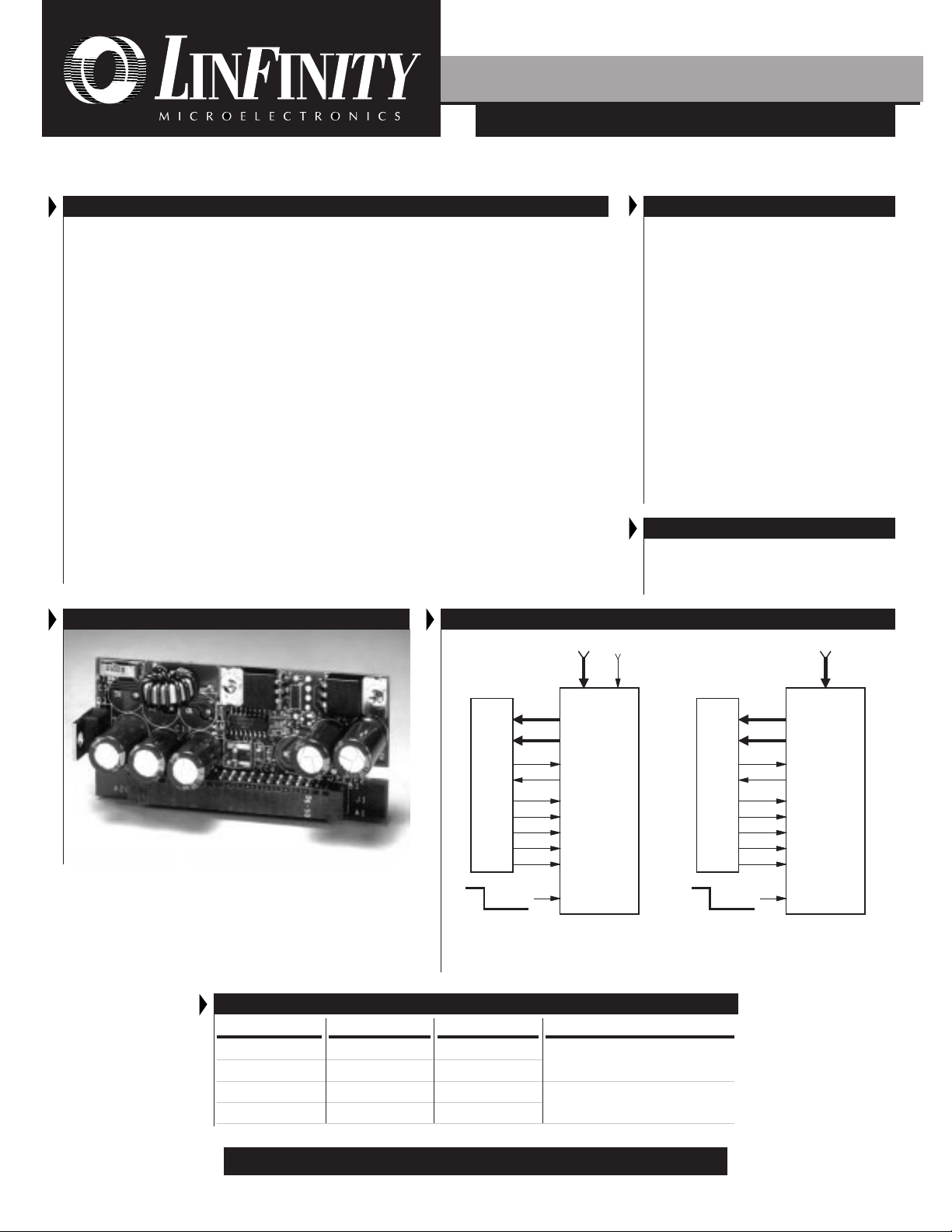
The LXM1700-05/1700A-05 powers
the processor using the 5V supply as
the input power and 12V for the
control bias. The LXM1700-12/
1700A-12 powers the processor using
only the 12V supply and does not need
a separate voltage for the control bias
(see Block Diagram below). The +5V
or the +12V input configuration is
factory set via simple jumper connections. The LXM1700-12/1700A-12 is
primarily used for multiple processor
applications, such as quad processor
servers, where 5V supplies may not
have the needed current capability.
PRELIMINARY DATA SHEET
■■
■ GUARANTEED 14.0A OUTPUT
■■
p TOTAL OUTPUT TOLERANCE OF LESS
THAN ±5% — Includes: Line & load
regulation, temperature stability, initial
accuracy, load transient and ripple & noise.
p ADJUSTABLE OUTPUT VOLTAGE USING A
FIVE-BIT WORD (See Table 1)
p OVER-VOLTAGE DETECTION CROWBARS
THE OUTPUT VOLTAGE IN THE EVENT OF
PASS TRANSISTOR FAILURE - 100%
PROCESSOR PROTECTION (LXM1700-xx)
p HIGH EFFICIENCY — 85% (TYP.)
p POWER GOOD SIGNAL INDICATES LOW
OUTPUT VOLTAGE
p SOFT-START ELIMINATES TURN-ON
OVERSHOOT
p SHORT-CIRCUIT PROTECTION
p OUTPUT ENABLE /SHUTDOWN
APPLICATIONS
■ PENTIUM II PROCESSOR
■ PENTIUM PRO PROCESSOR
■ ADVANCED MICROPROCESSOR SUPPLIES
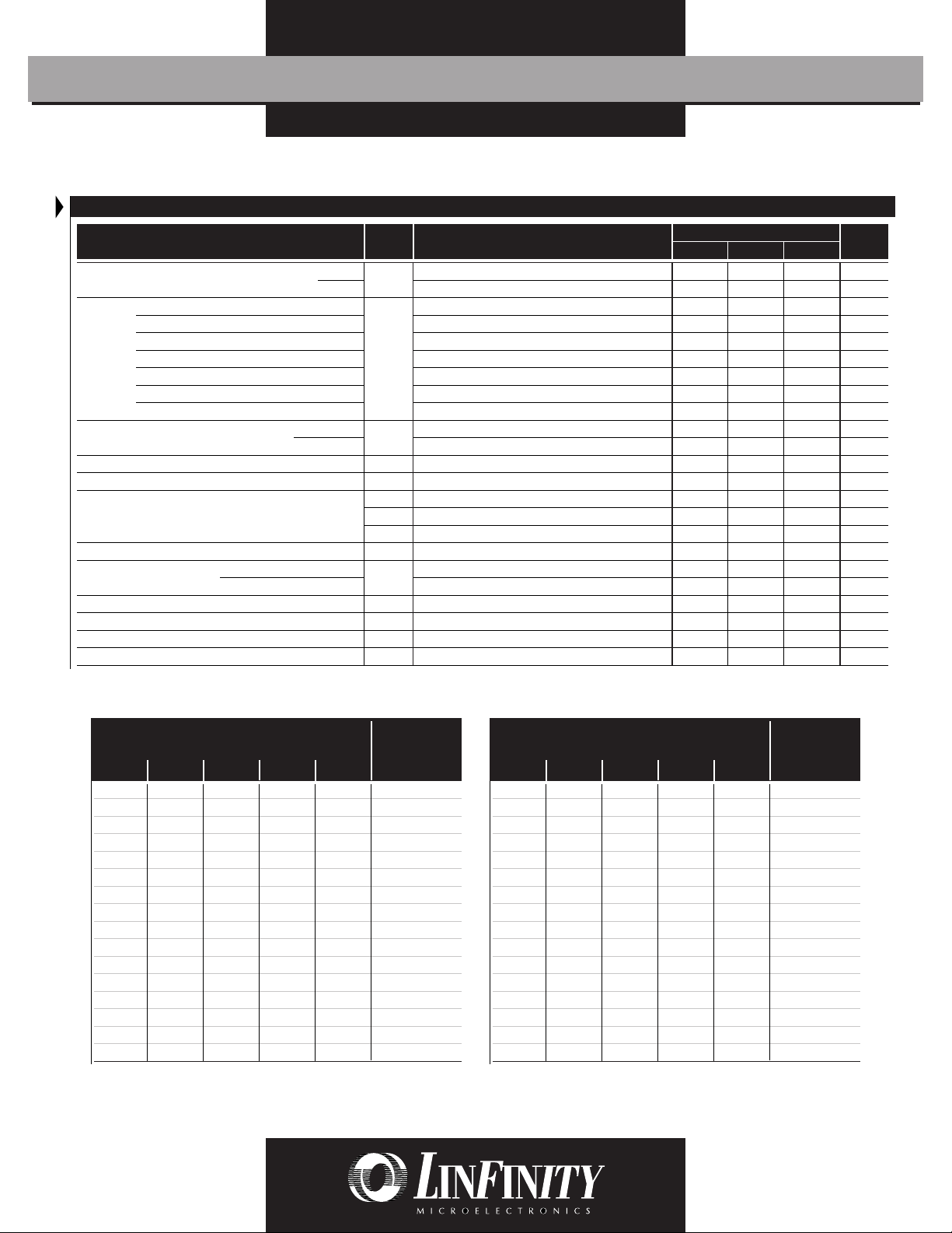
MODULE PHOTO
Part # Input I
LXM1700-05 +5V, +12V 14.0A
LXM1700-12 +12V 14.0A
LXM1700A-05 +5V, +12V 14.0A
LXM1700A-12 +12V 14.0A
BLOCK DIAGRAM
5V 12V
5V
12V
IN
V
CC (VID)
V
SS
UP#
µP
Disable
PWRGD
VID4
VID3
VID2
VID1
VID0
OUTEN
LXM1700-05/1700A-05
IN A +5V SUPPLY APPLICATION
MODULE ORDER INFORMATION
MAX
O.V. Protection Crowbar
IN
µP
LXM1700-05/1700A-05
Disable
LXM1700-12/1700A-12
IN A +12V SUPPLY APPLICATION
Yes
No
12V
12V
V
CCP (VID)
V
SS
UP#
PWRGD
VID4
VID3
VID2
VID1
VID0
OUTEN
IN
LXM1700-12/1700A-12
Copyright © 1997
Rev. 0.4 4/97
FOR FURTHER INFORMATION CALL (714) 898-8121
11861 WESTERN AVENUE, GARDEN GROVE, CA. 92841
1
Page 2
PRODUCT DATABOOK 1996/1997
LXM1700-xx/1700A-xx
P ENTIUM® II VRM MODULE
RELIMINARY DATA SHEET
P
ELECTRICAL CHARACTERISTICS
Parameter
Input Voltage Range +5V V
Total Output Voltage Tolerance VO3.1V Set Point
Includes:
Output Current Maximum I
Power Good Threshold V
Power Good Output LO Voltage R
Output Enable OUTEN
Turn-on Response T
Efficiency LXM1700-05/1700A-05 Eff I
Over-Voltage Threshold LXM1700-xx V
Average Short-Circuit Current I
Ambient Temperature T
Required Air Flow IO = 14.0A
Initial Accuracy IO = 0.5A, TA = 25°C
Load Regulation I
Line Regulation 0.95VIN to 1.05V
Temp. Stability 10 to 60°C
Load Transient IO = 0.5A to 14.0A, VIN = 5V
Output Ripple & Noise IO = 5A
Minimum
LO Level Input Voltage V
HI Level Input Voltage V
LXM1700-12/1700A-12 IO = 14.0A
Symbol
IN
+12V
O
THPG
LOPGISINK
OLIOL
OHIOH
R
OVVO
SC
A
Test Conditions Units
= 0.5A to 14.0A
O
IN
VO = 3.1V
= 5mA
= 1mA
= 1mA
0 to 99% of VO after VIN reaches 90%
= 14.0A
O
= 3.1V
VO = 0V
LXM1700-xx/1700A-xx
Min. Typ. Max.
4.75 5 5.25 V
11.4 12 12.6 V
2.945 3.1 3.255 V
±0.6 %
15 mV
1mV
16 mV
95 mV
12 mV
14.0 A
0A
0.93V
SET
0.4 V
0.8 V
2V
10 ms
80 85 %
80 85 %
3.41 3.57 3.72 V
2A
060°C
100 LFM
V
Table 1 - Voltage Identification Code
0 = Connected to VSS , 1 = Open or pull-up to V
Processor Pins
VID4 VID3 VID2 VID1 VID0 (VDC)
01111 *
01110 *
01101 *
01100 *
01011 *
01010 *
01001 *
01000 *
00111 *
00110 *
00101 1.80
00100 1.85
00011 1.90
00010 1.95
00001 2.00
00000 2.05
* Level reserved for future requirements; VRM8.1 output shall be disabled for these VID codes.
V
IN
CC (VID)
0 = Connected to VSS , 1 = Open or pull-up to V
Processor Pins
V
IN
CC (VID)
VID4 VID3 VID2 VID1 VID0 (VDC)
11111No CPU
11110 2.1
11101 2.2
11100 2.3
11011 2.4
11010 2.5
11001 2.6
11000 2.7
10111 2.8
10110 2.9
10101 3.0
10100 3.1
10011 3.2
10010 3.3
10001 3.4
10000 3.5
2
Copyright © 1997
Rev. 0.4 4/97
Page 3

PRODUCT DATABOOK 1996/1997
LXM1700-xx/1700A-xx
P ENTIUM® II VRM MODULE
P RELIMINARY DATA SHEET
CONNECTOR PIN-OUTS AND DESCRIPTIONS
Pin # Ref. Desig. Description
A1 5V
A2 5V
A3 5V
A4 12V
IN
IN
IN
IN
A5 Reserved This pin is reserved for future applications
A6 I
SHARE
A7 VID0 Bit 0 of the 5-bit input (see Table 1)
A8 VID2 Bit 2 of the 5-bit input (see Table 1)
A9 VID4 Bit 4 of the 5-bit input (see Table 1)
A10 V
A11 V
A12 V
A13 V
A14 V
A15 V
A16 V
A17 V
A18 V
A19 V
A20 V
CC (VID)
SS
CC (VID)
SS
CC (VID)
SS
CC (VID)
SS
CC (VID)
SS
CC (VID)
5V Input Power (not needed for LXM1700-12)
5V Input Power (not needed for LXM1700-12)
5V Input Power (not needed for LXM1700-12)
12V Input Power
Consult Factory
Output voltage to microprocessor
Output voltage return
Output voltage to microprocessor
Output voltage return
Output voltage to microprocessor
Output voltage return
Output voltage to microprocessor
Output voltage return
Output voltage to microprocessor
Output voltage return
Output voltage to microprocessor
Pin # Ref. Desig. Description
B1 5V
B2 5V
IN
IN
B3 Reserved This pin is reserved for future applications
B4 12V
IN
B5 UP # A TTL input indicates the presence of an
B6 OUTEN A TTL input that disables output when it
B7 VID1 Bit 1 of the 5-bit input (see Table 1)
B8 VID3 Bit 3 of the 5-bit input (see Table 1)
B9 PWRGD An open collector output that switches LO
B10 V
B11 V
B12 V
B13 V
B14 V
B15 V
B16 V
B17 V
B18 V
B19 V
B20 V
SS
CC (VID)
SS
CC (VID)
SS
CC (VID)
SS
CC (VID)
SS
CC (VID)
SS
5V Input Power (not needed for LXM1700-12)
5V Input Power (not needed for LXM1700-12)
12V Input Power
upgrade processor. LOW = Upgrade processor
switches to LO state
when output is below the specified range
Output voltage return
Output voltage to microprocessor
Output voltage return
Output voltage to microprocessor
Output voltage return
Output voltage to microprocessor
Output voltage return
Output voltage to microprocessor
Output voltage return
Output voltage to microprocessor
Output voltage return
0.188 (4.78)
TOP VIEW
FRONT
VIEW
(Facing Connector)
1.50
(38.1)
1.00
(25.4)
MODULE DIMENSIONS
3.10 (78.74)
2.725 (69.22)
0.30 (7.62) Max. 0.26 (6.60) Min.
Connector
0.065 (1.65) Ref
Power Board
Component Area
B20
A20
Note: All dimensions in inches (mm).
Connector
0.15 (3.81) Typical
Power
Board
0.42 (10.67) Typical
0.80
(20.32)
B1
A1
0.062 ±0.008
(1.58 ±0.20)
Copyright © 1997
Rev. 0.4 4/97
3
Page 4

PRODUCT DATABOOK 1996/1997
LXM1700-xx/1700A-xx
P ENTIUM® II VRM MODULE
RELIMINARY DATA SHEET
P
APPLICATION INFORMATION
3.3V
10K
10K
10K
10K
10K
CTRL
INPUTDCINPUT
10K
DISABLE (LO)
ENABLE (HI or Open)
Note: 10k pull-up resistors are optional and needed only in cases of noise suppression or long leads.
VID0
VID1
VID2
V
CC (VID)
GND
UP#
GND
VID3
VID4
P
OUTEN
GOOD
LXM1700/1700A
PART # DC INPUT CTRL INPUT
LXM1700-05/1700A-05 +5V +12V
LXM1700-12/1700A-12 +12V N.C.
FIGURE 1. — TYPICAL APPLICATION OF THE LXM1700-xx/1700A-xx
3.3V
PENTIUM
PRO
PROCESSOR
4.7K
VID Pins
0.1µf
Pentium is a registered trademark of Intel Corporation.
4
Copyright © 1997
Rev. 0.4 4/97
 Loading...