

Page 1
P
ATENT PENDING
LIN DOC #:
LXM1653-01
FLOATING OUTPUT DRIVE, CCFL INVERTER MODULES
1653
THE INFINITE POWER OF INNOVATION
DESCRIPTION KEY FEATURES
The LXM1653 floating output drive
CCFL (Cold Cathode Fluorescent Lamp)
Inverter Module is specifically designed
to drive large LCD displays (11.3" and
larger), which are used in notebook
computers. This new inverter was
specifically designed to reduce the
leakage currents from the lamp to the
reflector or the metal frame of the
panels. The floating output architecture of this inverter also permits a
much wider dimming range when
compared to non-floating designs, and
allows an additional 10% efficiency
improvement.
The module converts unregulated
DC voltage from the system battery or
AC adapter directly to high-frequency,
high-voltage sine waves required to
ignite and operate CCFL lamps. The
module design is based on a proprietary Linfinity IC that provides important new performance advances.
Remarkable improvements in
efficiency and RF emissions result from
this single stage resonant inverter,
featuring a patented
nous,
Zero Voltage Switching (CS-ZVS)
topology. CS-ZVS produces nearly
pure sine wave currents in the lamp,
Current Synchro-
PRODUCT HIGHLIGHT
enabling maximum light delivery, while
reducing both conducted and radiated
noise. This topology simultaneously
performs two tasks including line
voltage regulation and lamp dimming
through lamp current regulation.
These two functions are performed in
a single power stage made up of a pair
of low-loss MOSFETs. The MOSFETs
drive a low current resonant circuit that
feeds the primary of a high-voltage
transformer with a sinusoidal voltage.
Required L and C values in the
resonant circuit are such that very lowloss components can be used to obtain
higher electrical efficiency than is
possible with previous topologies.
The full-bridge LXM1653 provides
peak efficiency when operated at input
voltages from 6.5 volts to 18 volts.
In addition, this module is equipped
with a dimming input that permits full
range brightness control from an
external potentiometer or PWM signal,
and a sleep input that reduces module
power to a few microwatts in shutdown mode.
Output open and short circuit
protection are also featured on this
module.
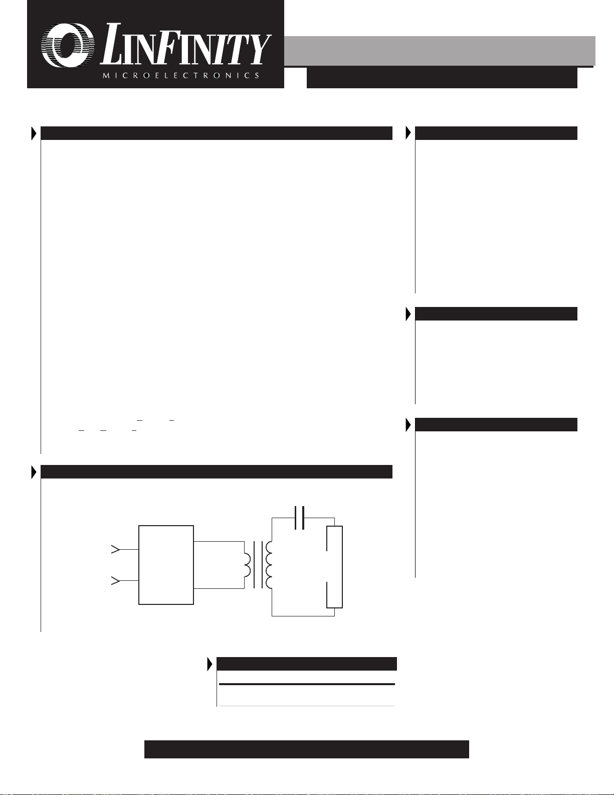
FLOATING OUTPUT ARCHITECTURE
High Voltage
Transformer
DC V
IN
Inverter
CS-ZVS
P RELIMINARY DATA SHEET
■ FULLY FLOATING OUTPUT
■ 35% MORE LIGHT OUTPUT AT 5 WATTS
■ GREATER EFFICIENCY THAN GROUNDED
OUTPUT DESIGNS
■ 6.5V TO 18V INPUT VOLTAGE RANGE
■ VERSATILE BRIGHTNESS CONTROL INPUT
■ 10 MICROAMP SLEEP CURRENT
■ OUTPUT SHORT CIRCUIT PROTECTION AND
AUTOMATIC OVER VOLTAGE LIMITING
■ 7.4mm MAX HEIGHT, NARROW FOOTPRINT
■ MINIMIZE THERMOMETER EFFECTS
■ MINIMIZE LAMP TO PANEL LEAKAGE
CURRENT
APPLICATIONS
■■
■ 11.3" LCD PANELS AND LARGER
■■
■■
■ NOTEBOOK AND SUB-NOTEBOOK
■■
COMPUTERS
■■
■ PORTABLE INSTRUMENTATION
■■
■■
■ AUTOMOTIVE DISPLAYS
■■
■■
■ DESKTOP DISPLAYS
■■
■■
■ AIRLINE ENTERTAINMENT CENTERS
■■
BENEFITS
■ ULTRA-HIGH EFFICIENCY, LINE VOLTAGE
REGULATION AND SLEEP MODE EXTEND
COMPUTER BATTERY LIFE
■ COOL OPERATION PERMITS CLOSE
PROXIMITY TO LCD PANEL WITHOUT
DISPLAY DISTORTION
■ SMOOTH, FULL-RANGE BRIGHTNESS
CONTROL GIVES YOUR PRODUCT A HIGH
QUALITY IMAGE
■ LOW EMI / RFI DESIGN MINIMIZES
SHIELDING REQUIREMENTS
■ NARROW, LOW-PROFILE MODULE FITS
CCFL
INTO MOST LCD ENCLOSURES
Copyright © 1997
Rev. 0.1 3/97
MODULE ORDER INFO
FULL-BRIDGE DRIVE
LXM1653-01
FOR FURTHER INFORMATION CALL (714) 898-8121
11861 WESTERN AVENUE, GARDEN GROVE, CA. 92841
1
Page 2
PATENT PENDING
PRODUCT DATABOOK 1996/1997
LXM1653-01
FLOATING OUTPUT DRIVE, CCFL INVERTER MODULES
RELIMINARY DATA SHEET
P
ABSOLUTE MAXIMUM RATINGS (Note 1)
Input Supply Voltage (VIN)......................................................................................................................................................... 6.5V to 18V
Output Voltage, no load ..............................................................................................................................Internally Limited to 2000V
Output Current .............................................................................................................................................. 7.5mA
Output Power ........................................................................................................................................................................................... 6W
Input Signal Voltage, (SLEEP and BRITE Inputs) .................................................................................................................. -0.3V to 6.5V
Ambient Operating Temperature, zero airflow ........................................................................................................................ 0°C to 60°C
Storage Temperature Range................................................................................................................................................... -40°C to 85°C
Note 1. Exceeding these ratings could cause damage to the device. All voltages are with respect to Ground. Currents are positive into, negative out of
the specified terminal.
RECOMMENDED OPERATING CONDITIONS (R.C.)
This module has been designed to operate over a wide range of input and output conditions. However, best efficiency and performance
will be obtained if the module is operated under the condition listed in the 'R.C.' column. Min. and Max. columns indicate values beyond
which the inverter, although operational, will not function optimally.
Parameter
Symbol
Input Supply Voltage
Output Power P
Brightness Control Input Voltage Range V
Lamp Operating Voltage V
Lamp Current - Full Brightness I
Operating Ambient Temperature Range T
O
BRITE
LAMP
OLAMP
A
Recommended Operating Conditions
Min. R.C. Max.
6.5 18 V
4.0 6.0 W
0.0 2.0 V
300 600 800 V
7.2 mA
060°C
(Internally Limited)
RMS
RMS
Units
RMS
RMS
ELECTRICAL CHARACTERISTICS
Unless otherwise specified, these specifications apply over the recommended operating conditions and 25°C ambient temperature for the LXM1653.
Parameter
Symbol
Test Conditions Units
LXM1653
Min. Typ. Max.
Output Pin Characteristics
Full Bright Lamp Current I
Minimum Lamp Current I
L (MAX)VBRITE
L (MIN)VBRITE
Lamp Start Voltage VLS0°C < TA < 60°C
Operating Frequency f
O
= 2.0 VDC, V
V
= 2.0 VDC, V
BRITE
V
= 2.0 VDC, V
BRITE
V
= 2.0 VDC, V
BRITE
= 0.0 V
V
= 2.5VDC, SLEEP = Logic High, VIN = 12V
BRITE
= 750V
LAMP
= 750V
LAMP
= 350V
LAMP
= 600V
LAMP
DC
RMS
RMS
RMS
RMS
, V
, V
, V
, V
IN
IN
IN
IN
≥ 10.8V
≥ 9.0V
≥ 6.5V
≥ 8.0V
DC
DC
DC
DC
6.8 7.2 7.7 mA
5.0 5.5 mA
6.8 7.2 mA
6.8 7.2 mA
2.5 mA
1800 V
55 60 65 KHz
Brightness Control
Input Current I
BRITEVBRITE
Input Voltage for Max. Lamp Current VCI
Input Voltage for 50% Lamp Current V
CIO (LAMP)
= 0V
O (LAMP)
DC
= 100%
= 50%
-200 -1000 nA
2.4 2.5 2.6 V
1.25 V
SLEEP Input
Input Logic 1 V
Input Logc 0 V
Input Current I
IH
IL
V
SLEEP
= 0 - 5V
DC
IN
2.5 5.5 V
0 0.8 V
50 100 µA
Voltage Reference
Output Voltage V
Output Current I
0 < I
REF
REF
< 500µA
REF
2.40 2.50 2.60 V
500 µA
Power Characteristics
Sleep Current I
IN (MIN)VIN
= 12V, SLEEP = Logic 0 10 30 µA
RMS
RMS
DC
DC
DC
DC
DC
DC
DC
DC
DC
2
Copyright © 1997
Rev. 0.1 3/97
Page 3

PRODUCT DATABOOK 1996/1997
FLOATING OUTPUT DRIVE, CCFL INVERTER MODULES
Conn. Pin Description
CN1
CN1-1
CN1-2
CN1-3
CN1-4
CN1-5
CN1-6
CN1-7
CN1-8
CN2
CN2-1
CN2-2
V
IN
Input voltage. (+6.5 to +18VDC)
GND Power supply return.
SLEEP Logical high on this pin enables inverter operation. Logical low removes power from the module and
the lamp. A floating input is sensed as a logical low and will disable inverter operation. If not used,
connect SLEEP to VIN.
BRITE Brightness control input. Apply 0.0 to 2.0 volts DC to control lamp brightness. Lamp current varies
linearly with input voltage. Open circuit or 2.0V gives maximum brightness. This input may also be
driven with a PWM logic signal. See Application Notes Section.
AGND Brightness control signal return. For best results do not run V
V
REF
Reference Voltage Output. 2.5V @ 500µA max. For use with external dimming circuit.
LAMP HI High-voltage connection to high side of lamp. Connect to lamp terminal with shortest lead length. Do
not connect to ground.
LAMP LO High-voltage connection to low side of lamp. Connect to lamp terminal with longer lead length.
This lead may be safely connected to ground, but may not result in specified performance depending on
system wiring and lamp characteristics.
P RELIMINARY DATA SHEET
FUNCTIONAL PIN DESCRIPTION
power supply return current through this pin.
IN
PATENT PENDING
LXM1653-01
APPLICATION DIAGRAM
9.0
8.0
)
RMS
- (mA
LAMP
I
7.0
6.0
5.0
4.0
3.0
RMS
350V
6
7891018
LAMP
V
0V
= 60
RMS
LAMP
V
0V
= 65
RMS
LAMP
V
0V
= 70
RMS
V
RMS
0V
= 76
LAMP
VIN - (Volts DC)
FIGURE 1 — MAXIMUM LAMP CURRENT vs. INPUT VOLTAGE FOR TYPICAL LAMP VOLTAGES
Copyright © 1997
Rev. 0.1 3/97
3
Page 4

PATENT PENDING
e
LXM1653-01
Sytem Battery
(NiCd, NiMH, etc.)
Management
AC/DC
Adapter
From Power
Logic
PRODUCT DATABOOK 1996/1997
FLOATING OUTPUT DRIVE, CCFL INVERTER MODULES
RELIMINARY DATA SHEET
P
TYPICAL APPLICATIONS
3.3 or 5V
CMOS
or TTL
100k
R
1
R2, 25k
V
REF
BRITE
SLEEP
AGND
V
IN
LXM1653
LAMP HI
LAMP LO
GND
CFL
TUBE
Insid
LCD
Panel
From Logic
(optional)
S1
"Increase"
S2
"Decrease"
N.O.
N.O.
47k
47k
FIGURE 21 — NOTEBOOK SYSTEM APPLICATION
12V
DC
V
IN
LAMP HI
1K TO
100K
2.0V
DC
BRITE
LXM1653
ON / OFF
+5V
SLEEP
GND
FIGURE 22 — POTENTIOMETER BRIGHTNESS CONTROL
+5V
LAMP LO
U1
R
UC
D
DC
RH
RW
RL
1
V
REF
BRITE
AGND
LXM1653
+5V
FIGURE 23 — NONVOLATILE DIGITAL BRIGHTNESS CONTROL
CCFL
TUBE
• S1 & S2 are momentary push buttons,
normally open contacts.
• U1 = 100k digital pot.
• R
value optional for choosing dimming
1
range.
4
Copyright © 1997
Rev. 0.1 3/97
Page 5

PRODUCT DATABOOK 1996/1997
FLOATING OUTPUT DRIVE, CCFL INVERTER MODULES
P RELIMINARY DATA SHEET
TYPICAL APPLICATIONS (continued)
12V
DC
V
PWM
IN
BRITE
LAMP HI
PATENT PENDING
LXM1653-01
ON / OFF
LXM1653
SLEEP
PWM
PULSE
WIDTH
10µsec £ Period £ 100µsec
0 £ Pulse Width £ Period
FIGURE 24 — PWM BRIGHTNESS CONTROL
GND
Period
LAMP LO
CCFL
TUBE
Copyright © 1997
Rev. 0.1 3/97
5
Page 6

PATENT PENDING
5.35 (136)
5.256 (133.5)
0.512
(13.0)
2-1
CN-1
1-1
0.060 (1.52)
All dimensions in inches (mm)
0.291 (7.40) Max.
Warning!!
High Voltage
Present
.089 (2.25)
.089
(2.25)
Ø 0.089 (2.26)
Dia. Mtg. Hole 2 Plcs
1
1
L1
T1
CN-2
.256 (6.5)
Conn
Entry
Conn
Entry
LXM1653-01
PRODUCT DATABOOK 1996/1997
FLOATING OUTPUT DRIVE, CCFL INVERTER MODULES
RELIMINARY DATA SHEET
P
PHYSICAL DIMENSIONS
LXM1653
CN-1 = MOLEX P/N: 53261-0890
CN-2 = JST P/N: SM02-(8.0)B-BHS-1D
6
Copyright © 1997
Rev. 0.1 3/97
 Loading...