

Page 1
A
LIN DOC #:
LX8940
8940
5V L
T HE I NFINITE P OWER OF I NNOVATION
DESCRIPTION KEY FEATURES
The LX8940 is a 5V, low dropout, low
quiescent current regulator rated for 1A
of output current. It can regulate with
as low as 0.4V headroom between the
input and output voltages, thus
minimizing power dissipation. In
addition, it can be used in applications
where worst case supplies require a
NOTE: For current data & package dimensions, visit our web site: http://www.linfinity.com.
PRODUCT HIGHLIGHT
5.3V
IN
LX8940
low input-output differential to maintain
regulation. This feature makes it ideal
for computer monitors that have to
comply with energy-efficient / "Green
PC" programs, where the input voltage
drops to only a few tenths of a volt
above the output when power supply
enters sleep-mode operation.
OUT
GND
5V/100m
10µF0.1µF
OW DROPOUT REGULATOR
P RODUCTION DATA SHEET
■■
■ 2% Internally Trimmed Output
■■
■■
■ Output Current In Excess Of 1A
■■
■■
■ Input-Output Differential
■■
Less Than 0.4V At 1A
p Reverse Battery Protection
p 60V Load Dump Protection
p -50V Reverse Transient Protection
p Short Circuit Protection
p Internal Thermal Overload Protection
p Available In 3-Lead Plastic TO-220
p Drops In Most lM2940 Sockets
APPLICATIONS
■ Small Headroom Battery Applications
■ High Efficiency Linear Regulators
■ Post Regulators For Switching Power
Supplies
■ Green PC Monitor Applications
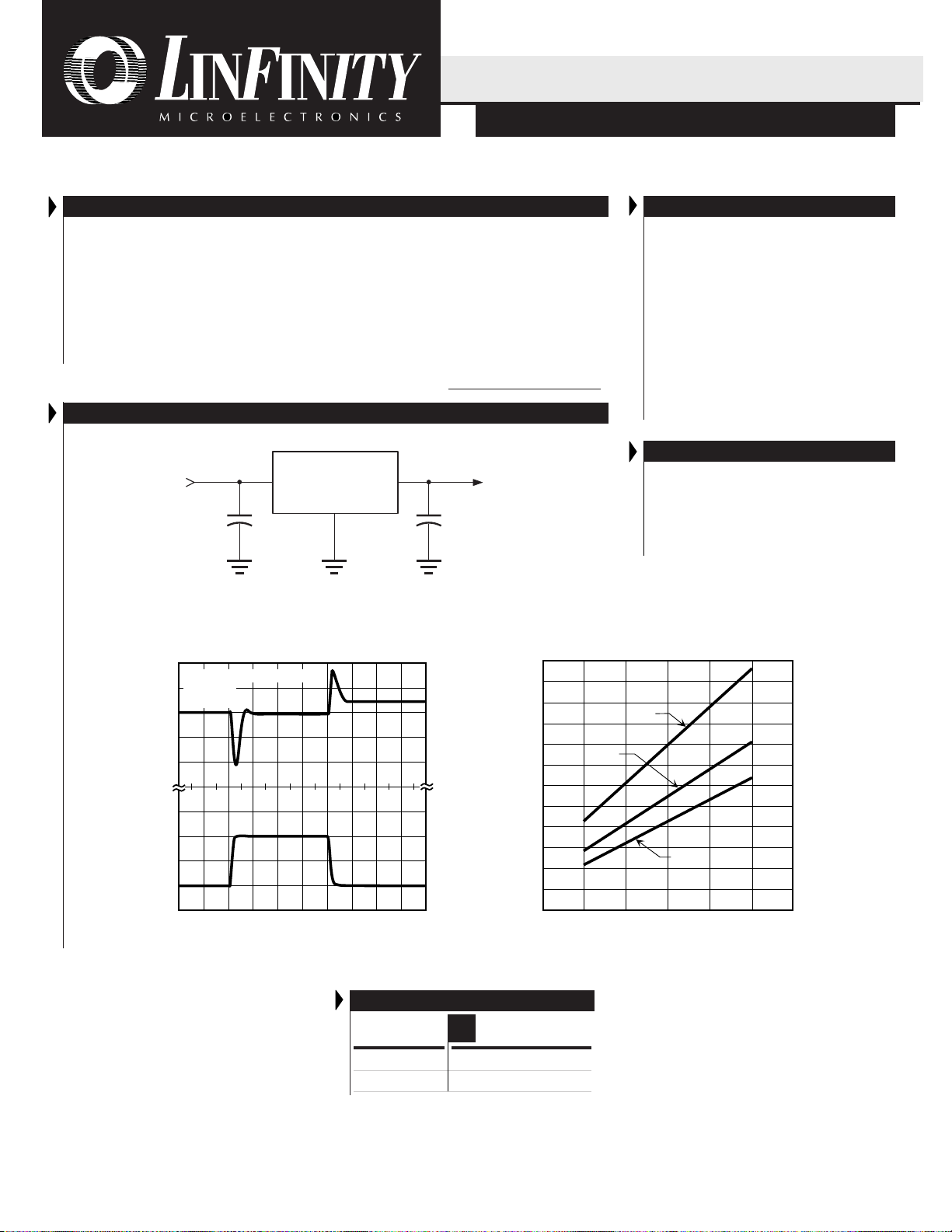
L OAD TRANSIENT RESPONSE
TA = 25°C
C
= 1µF
IN
= 5.30V
V
IN
5.000V
(20mV / Div.)
Output Voltage
4.980V
100mA
(50mA / Div.)
0mA
Output Current
CO = 47µF Electrolytic
Time - (20µs/Div.)
DROPOUT VOLTAGE VS. OUTPUT CURRENT
600
500
400
300
200
Dropout Voltage - (mV)
100
0
PACKAGE ORDER INFO
TA (°C)
0 to 125 LX8940CP
-40 to 125 LX8940IP
Plastic TO-220
P
3-pin
VS
. TEMPERATURE
125°C
25°C
100
Output Current - (mA)
500
-40°C
1000
Copyright © 1999
Rev. 1.3 3/99
L INF INITY MICROELECTRONICS INC.
11861 WESTERN AVENUE, GARDEN GROVE, CA. 92841, 714-898-8121, FAX: 714-893-2570
1
Page 2
LX8940
PRODUCT DATABOOK 1996/1997
5V L
OW DROPOUT REGULATOR
RODUCTION DATA SHEET
P
ABSOLUTE MAXIMUM RATINGS (Note 1)
Input Voltage (VIN) .......................................................................................... -15V to 26V
Operating Junction Temperature
Plastic (P Package) ................................................................................................ 150°C
Storage Temperature Range ...................................................................... -65°C to 150°C
Lead Temperature (Soldering, 10 seconds) ............................................................. 300°C
Note 1. Exceeding these ratings could cause damage to the device. All voltages are with respect
to Ground. Currents are positive into, negative out of the specified terminal. Pin
numbers refer to DIL packages only.
THERMAL DATA
P PACKAGE:
THERMAL RESISTANCE-JUNCTION TO TAB,
THERMAL RESISTANCE-JUNCTION TO AMBIENT,
Junction Temperature Calculation: TJ = TA + (P
The θ
numbers are guidelines for the thermal performance of the device/pc-board system.
JA
All of the above assume no ambient airflow.
θθ
θ
θθ
JT
θθ
θ
θθ
JA
x θ
).
D
JA
3.0°C/W
60°C/W
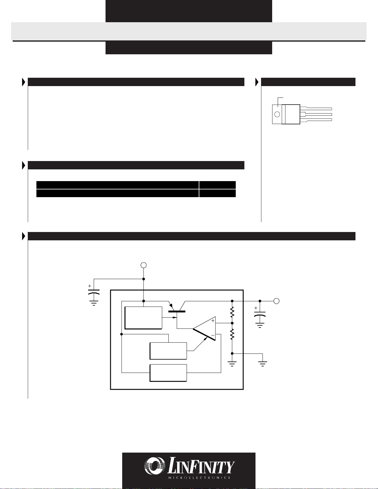
PACKAGE PIN OUTS
Tab is GROUND
3
2
1
P PACKAGE
(Top View)
OUTPUT
GND
INPUT
C1*
0.1µF
INPUT VOLTAGE
1 (INPUT)
OVERVOLTAGE
THERMAL
SHUTDOWN
REGULATOR
REFERENCE
BLOCK DIAGRAM
LX8940
BIAS
1.23V
* Required if regulator is located far from power supply filter.
3 (OUTPUT)
OUTPUT VOLTAGE
C2
10µF
2 (GND)
2
Copyright © 1999
Rev. 1.3 3/99
Page 3

PRODUCT DATABOOK 1996/1997
LX8940
5V L
OW DROPOUT REGULATOR
P RODUCTION DATA SHEET
RECOMMENDED OPERATING CONDITIONS
Parameter
Input Voltage V
Symbol
IN
Load Current (with adequate heatsinking)
Maximum Line Transient (Load Dump), V
≤ 5.5V
O
Input Capacitor (VIN to GND)
Output Capacitor with ESR of 10Ω max., (V
Note 2. V
IN (MIN)
= 1.2∆V
. See Dropout Voltage maximum limit.
(MAX)
to GND & VSB to GND)
OUT
ELECTRICAL CHARACTERISTICS
Unless otherwise specified, these specifications apply over the operating ambient temperatures of -40°C to +125°C for LX8940IP, and 0°C to +125°C
for LX8940CP; VIN = 10V, IO = 1A, C
junction and case temperatures equal to the ambient temperature.)
Parameter
Output Voltage VOIO = 0A, TA = 25°C
Line Regulation ∆VOI7V ≤ VIN ≤ 26V, I
Load Regulation ∆VOL50mA ≤ IO ≤ 1A
Output Impedance (Note 3) r
Quiescent Current I
Output Noise Voltage (Note 3) V
Long Term Stability (Note 3)
Ripple Rejection (Note 3) RRfO = 120Hz, 1V
Dropout Voltage ∆VI
Current Limit I
Maximum Operational Input Voltage V
Maximum Line Transient VIN
Note 3. These parameters, although guaranteed, are not tested in production.
= 22µF, and are for DC characteristics only. (Low duty cycle pulse testing techniques are used which maintains
OUT
Symbol
O
QIO
100mADC and 20mA
≤ 5mA, 7 ≤ VIN ≤ 26V
Test Conditions Units
= 5mA
O
, fO = 120Hz
RMS
IO = 500mA
IO = 1000mA
10Hz - 100kHz, IO = 5mA
O RMS
, IO = 100mA
= 100mA
O
RMS
IO = 500mA
IO = 1A
VIN = 26V
CL
IN (MAX)
= 100Ω, T ≤ 100ms
(TR)RO
Recommended Operating Conditions
Min. Typ. Max.
Note 2 26 V
5 1000 mA
60 V
0.1 µF
10 µF
LX8940
Min. Typ. Max.
4.85 5 5.15 V
150 mV
10 50 mV
200 mΩ
315 mA
30 50 mA
115 180 mA
150 µV
20 mV/1000hr
66 dB
150 300 mV
275 500 mV
400 800 mV
1 1.2 A
26 31 V
60 V
Units
RMS
Copyright © 1999
Rev. 1.3 3/99
3
Page 4

LX8940
PRODUCT DATABOOK 1996/1997
5V L
The advantages of using a low-dropout regulator such as the
LX8940 is the need for less “headroom” for full regulation, and the
inherent reverse polarity protection provided by the PNP output
device. A typical NPN regulator design requires an input to output
differential of approximately two volts minimum. This is due to
the 2Vbe + Vcesat of the NPN Darlington used in the output,
coupled with the voltage drop across the current limit resistor. In
contrast, the “PNP Regulator” uses a single series pass transistor
with its single Vcesat, thus the lower input to output voltage
differential or dropout voltage.
In some applications the regulator output voltage is used not
only as a power supply but also as a voltage reference for control
systems. In such cases not just the temperature stability of the
output is important but also the initial accuracy. LX8940 fills this
need as the internal bandgap reference is trimmed allowing a
typical output voltage tolerance of ±1%.
EXTERNAL CAPACITORS
To stabilize the outputs and prevent oscillation (perhaps by many
volts) external capacitors are required. The minimum recommended value for the output capacitors is 10µF, although the
actual size and type will likely vary according to the particular
application, e.g., operating temperature range and load. Another
consideration is the effective series resistance (ESR) of the
OW DROPOUT REGULATOR
RODUCTION DATA SHEET
P
APPLICATION NOTES
capacitor. Capacitor ESR will vary by manufacturer. Consequently, some evaluation may be required to determine the
minimum value of the output capacitors. Generally worst case
occurs at the maximum load and minimum ambient temperature.
The size of the output capacitor can be increased to any value
above the minimum. One possible advantage of this would be to
maintain the output voltage during brief periods of negative input
transients
The output capacitors chosen should be rated for the full range
of ambient temperature over which the circuit will be exposed and
expected to operate. For example, many aluminum type electrolytic capacitors change values at cold temperatures. The effective
capacitance is reduced and regulator stability is effected. Tantalum capacitors are a good choice for these types of environments.
OUTPUT PROTECTION
The output features fault protection against overvoltage as well as
a thermal shutdown feature. If the input voltage rises above 33V
(load dump), the output shuts down automatically. The internal
circuitry is thus protected and the IC is able to survive higher
voltage transients than might otherwise be expected. The thermal
shutdown output effectively guards against overheating of the die
and protects the device from being damaged.
PRODUCTION DATA - Information contained in this document is proprietary to LinFinity, and is current as of publication date. This document
may not be modified in any way without the express written consent of LinFinity. Product processing does not necessarily include testing of
all parameters. Linfinity reserves the right to change the configuration and performance of the product and to discontinue product at any time.
4
Copyright © 1999
Rev. 1.3 3/99
 Loading...