

Datasheet LX6431IDM, LX6431CLP, LX6431CDM, LX6431BILP, LX6431BIDM Datasheet (Microsemi Corporation)
...Page 1
LX6431/LX6431A/LX6431B
A
P
RECISION PROGRAMMABLE REFERENCES
T HE I NFINITE P OWER OF I NNOVATION
DESCRIPTION KEY FEATURES
The LX6431 series precision adjustable
three terminal shunt voltage regulators are
pin-to-pin compatible with the industry
standard TL431, but with significant
improvements. The LX6431 design has
eliminated regions of instability common
to older generation shunt regulator
products like the TL431. Designs are
made simpler by eliminating the task of
insuring capacitive loads, and output
voltage and cathode currents don't
combine for unstable operation. The
capacitor value is chosen simply to give
the best load transient response without
the possibility of instability. A lower
reference input current allows the use of
higher value reference divider resistors,
NOTE: For current data & package dimensions, visit our web site: http://www.linfinity.com.
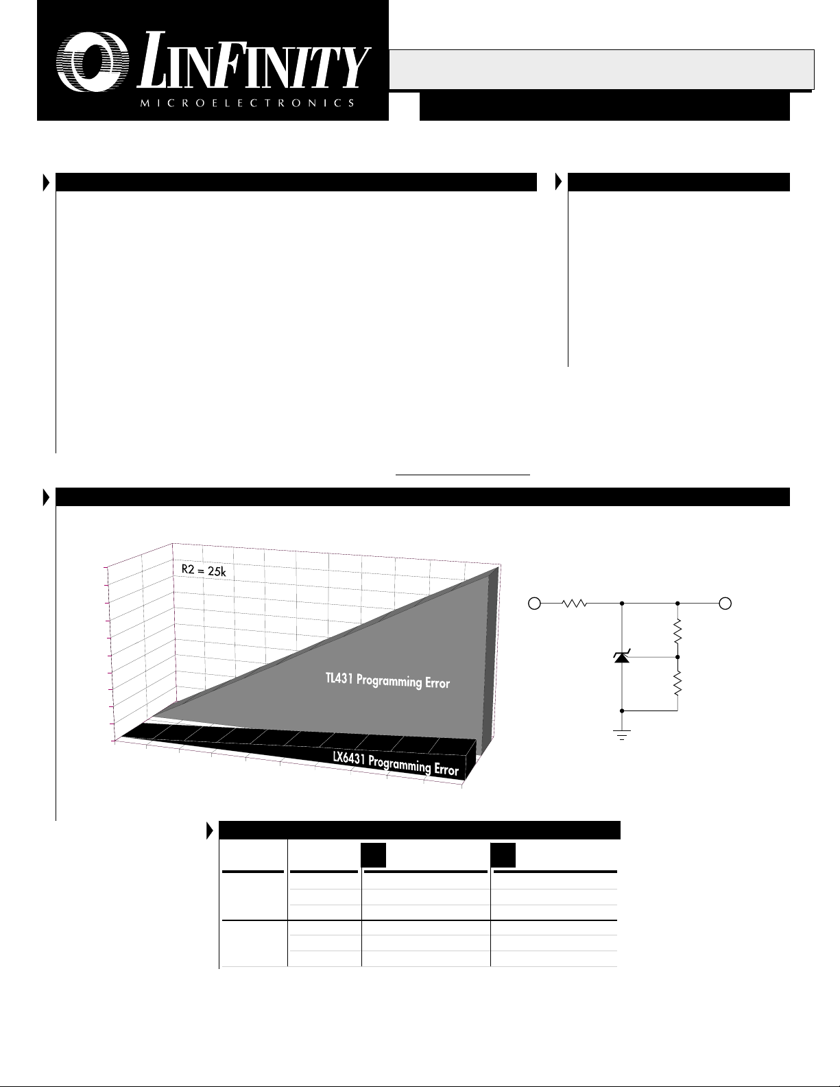
OUTPUT VOLTAGE ERROR DUE TO I
reducing the current drain from batteries
in portable equipment as well as reducing
the voltage programming errors due to
the impedance of the divider network
(See Product Highlight figure below). In
addition, the LX6431B has an improved
initial accuracy of 0.4%, and the output
voltage is programmable by using two
external resistors from 2.5V to 36V.
These devices offer low output
impedance for improved load regulation.
The typical output impedance of these
devices is 100mΩ. The reduced
reference input bias current and minimum
operating currents make these devices
suitable for portable and micropower
applications.
PRODUCT HIGHLIGHT
REF
P RODUCTION DATA SHEET
■ Unconditionally Stable For All Cathode To
Anode Capacitance Values
■ Reduced Reference Input Current Allowing
The Use Of Higher Value Divider Resistors
(0.5µA Max.)
■ Initial Voltage Reference Accuracy Of 0.4%
(LX6431B)
■ Sink Current Capability 0.6mA to 100mA
■ Typical Output Dynamic Impedance Less
Than 100mΩ
■ Adjustable Output Voltage From 2.5V to
36V
% Error
20
18
16
14
12
10
TYPICAL PROGRAMMABLE VOLTAGE
REFERENCE CIRCUIT
V
IN
R1
LX6431
8
6
4
2
0
2.5
3.75
5
6.25
7.5
8.75
10
11.25
12.5
(V ) OutputVoltage - (V)
KA
13.75
15
GND
R2
PACKAGE ORDER INFORMATION
(°C)
T
A
0 to 70 1% LX6431ACDM LX6431ACLP
-40 to 85 1% LX6431AIDM LX6431AILP
Initial
Tolerance
2% LX6431CDM LX6431CLP
0.4% LX6431BCDM LX6431BCLP
2% LX6431IDM LX6431ILP
0.4% LX6431BIDM LX6431BILP
Note: All surface-mount packages are available in Tape & Reel.
Append the letter "T" to part number. (i.e. LX5212CDPT)
TO-92 (LP) package also available in ammo-pack.
Plastic SOIC
DM
8-pin
Plastic TO-92
LP
3-pin
V
K
Copyright © 1999
Rev. 1.4 6/99
L INF INITY MICROELECTRONICS INC.
11861 WESTERN AVENUE, GARDEN GROVE, CA. 92841, 714-898-8121, FAX: 714-893-2570
1
Page 2
PRODUCT DATABOOK 1996/1997
LX6431/LX6431A/LX6431B
P
RECISION PROGRAMMABLE REFERENCES
P RODUCTION DATA SHEET
ABSOLUTE MAXIMUM RATINGS (Note 1)
Cathode to Anode Voltage (VKA) ................................................................... -0.3V to 37V
Reference Input Current (I
Continuous Cathode Current (I
Operating Junction Temperature
) .................................................................... -50µA to 10µA
REF
) ......................................................... -100mA to 150mA
K
Plastic (DM & LP Packages) ................................................................................. 150°C
Storage Temperature Range ...................................................................... -65°C to 150°C
Lead Temperature ..................................................................................................... 300°C
Note 1. Exceeding these ratings could cause damage to the device. All voltages are with respect
to Ground. Currents are positive into, negative out of the specified terminal. Pin
numbers refer to DIL packages only.
THERMAL DATA
DM PACKAGE:
THERMAL RESISTANCE-JUNCTION TO AMBIENT,
LP PACKAGE:
THERMAL RESISTANCE-JUNCTION TO AMBIENT,
Junction Temperature Calculation: TJ = TA + (PD x θJA).
The θJA numbers are guidelines for the thermal performance of the device/pc-board system.
All of the above assume no ambient airflow
θθ
θ
θθ
JA
θθ
θ
θθ
JA
165°C/W
156°C/W
BLOCK DIAGRAM
PACKAGE PIN OUTS
CATHODE
N.C.
ANODE
N.C.
1 8
2 7
3 6
4 5
DM PACKAGE
(Top View)
LP PACKAGE
(Top View)
REF
ANODE
ANODE
N.C.
1. CATHODE
2. ANODE
3. REF
Ref (R)
Cathode (K)
V
REF
Anode (A)
2
Copyright © 1999
Rev. 1.4 6/99
Page 3
PRODUCT DATABOOK 1996/1997
LX6431/LX6431A/LX6431B
P
RECISION PROGRAMMABLE REFERENCES
P RODUCTION DATA SHEET
ELECTRICAL CHARACTERISTICS (Note 2)
(Unless otherwise specified, these specifications apply over the operating ambient temperatures for LX6431C/LX6431AC/LX6431BC with 0°C ≤ TA ≤
70°C, LX6431I/LX6431AI/LX6431BI with -40°C ≤ TA ≤ 85°C.)
Parameter
Reference Input Voltage LX6431 V
LX6431A I
LX6431B IK = 10mA, VKA = V
Reference Drift LX6431 IK = 10mA, VKA = V
LX6431A I
LX6431B IK = 10mA, VKA = V
Symbol
REFIK
= 10mA, VKA = V
= 10mA, VKA = V
K
= 10mA, VKA = V
I
K
= 10mA, VKA = V
K
IK = 10mA, VKA = V
IK = 10mA, VKA = V
Test Conditions
, TA = 25°C,
REF
, TA = 25°C
REF
, TA = 25°C
REF
, 0°C ≤ TA ≤ 70°C
REF
, -40°C ≤ TA ≤ 85°C
REF
, 0°C ≤ TA ≤ 70°C
REF
, -40°C ≤ TA ≤ 85°C
REF
, 0°C ≤ TA ≤ 70°C
REF
, -40°C ≤ TA ≤ 85°C
REF
Voltage Ratio, Reference to Cathode IK = 10mA, VKA = 2.5V to 36V, TA = 25°C
(Note 3) IK = 10mA, VKA = 2.5V to 36V, TA = Operating Range
Reference Input Current I
Minimum Operating Current I
Off-State Cathode Current I
Dynamic Impedance Z
REF
MIN
OFF
KAVKA
VKA = V
, TA = 25°C
REF
VKA = V
, TA = Operating Range
REF
VKA = V
to 36V, TA = 25°C
REF
VKA = V
to 36V, TA = Operating Range
REF
VKA = 36V, V
= V
= 0V, TA = 25°C
REF
, IK = 0.6mA to 100mA, f ≤ 1kHz, TA = 25°C
REF
Note 2. These parameters are guaranteed by design.
∆V
Note 3. Ratio of change in reference input voltage
REF
∆V
KA
to the change in cathode voltage.
LX6431
Min. Typ. Max.
Units
2440 2550 mV
2470 2520 mV
2490 2510 mV
15 mV
25 mV
15 mV
25 mV
15 mV
20 mV
0.3 1 mV/V
0.3 1 mV/V
0.1 0.5 µA
0.1 0.5 µA
0.4 0.6 mA
0.4 0.6 mA
0.3 1 µA
30 100 mΩ
Copyright © 1999
Rev. 1.4 6/99
3
Page 4

PRODUCT DATABOOK 1996/1997
LX6431/LX6431A/LX6431B
P
RECISION PROGRAMMABLE REFERENCES
P RODUCTION DATA SHEET
GRAPH / CURVE INDEX
Characteristic Curves
FIGURE #
1. REFERENCE VOLTAGE vs. FREE-AIR TEMPERATURE
2. REFERENCE CURRENT vs. FREE-AIR TEMPERATURE
3. CATHODE CURRENT vs. CATHODE VOLTAGE
4. OFF-STATE CATHODE CURRENT vs. FREE-AIR TEMPERATURE
5. RATIO OF DELTA REFERENCE VOLTAGE TO DELTA CATHODE
VOLTAGE vs. FREE-AIR TEMPERATURE
6. EQUIVALENT INPUT NOISE VOLTAGE vs. FREQUENCY
FIGURE INDEX
Application Information
FIGURE #
7. COMPARISON OF REFERENCE RESISTOR VALUES BETWEEN AN
LX6431B AND A TL1431. Resistors used with the LX6431B are 5
times higher in value.
8. COMPARISON OF REFERENCE RESISTOR VALUES BETWEEN AN
LX6431B AND A TL1431. When used as 0.5%, 5V shunt
regulators.
Parameter Measurement Information
FIGURE #
9. TEST CIRCUIT FOR V
10. TEST CIRCUIT FOR VKA > V
11. TEST CIRCUIT FOR I
= V
KA
REF
REF
OFF
Typical Characteristics
FIGURE #
12. EQUIVALENT INPUT NOISE VOLTAGE OVER A 10-SECOND PERIOD
13. SMALL-SIGNAL VOLTAGE AMPLIFICATION vs. FREQUENCY
14. REFERENCE IMPEDANCE vs. FREQUENCY
15. PULSE RESPONSE
16. DIFFERENTIAL VOLTAGE AMPLIFICATION vs. FREQUENCY
4
Copyright © 1999
Rev. 1.4 6/99
Page 5

PRODUCT DATABOOK 1996/1997
0.2
0
(TA) Ambient Temperature - (°C)
0.8
(I
OFF
) Off-State Cathode Current - (µA)
0.4
-50
-25 0
25
50 75 100 125
0.6
VKA = 36V
V
REF
= 0
0.1
0.3
0.5
0.7
LX6431/LX6431A/LX6431B
P
RECISION PROGRAMMABLE REFERENCES
P RODUCTION DATA SHEET
CHARACTERISTIC CURVES
FIGURE 1. — REFERENCE VOLTAGE
vs. FREE-AIR TEMPERATURE
2.52
V
= V
REF
KA
IK = 10mA
2.51
2.50
) Reference Voltage - (V)
2.49
REF
(V
2.48
-50
-25 0
25
(TA) Ambient Temperature - (°C)
50 75 100 125
FIGURE 2. — REFERENCE CURRENT
vs. FREE-AIR TEMPERATURE
0.15
IK = 10mA
R1 = 10k
0.14
0.13
0.12
) Reference Current - (µA)
REF
0.11
(I
0.1
-50
-25 0
25
(TA) Ambient Temperature - (°C)
50 75 100 125
FIGURE 3. — CATHODE CURRENT vs. CATHODE VOLTAGE FIGURE 4. — OFF-STATE CATHODE CURRENT
vs. FREE-AIR TEMPERATURE
800
VKA = V
REF
TA = 25°C
600
400
200
) Cathode Current - (µA)
K
(I
0
-200
-1 0
-2
(VKA) Cathode Voltage - (V)
Copyright © 1999
Rev. 1.4 6/99
1
234
5
Page 6

PRODUCT DATABOOK 1996/1997
120
100
(f) Frequency - (Hz)
260
(V
N
) Noise Voltage - (nV/ Hz)
140
10 100
1k
10k 100k
200
220
160
180
240
IO = 10mA
T
A
= 25°C
LX6431/LX6431A/LX6431B
P
RECISION PROGRAMMABLE REFERENCES
P RODUCTION DATA SHEET
CHARACTERISTIC CURVES
FIGURE 5. — RATIO OF DELTA REFERENCE VOLTAGE TO DELTA
CATHODE VOLTAGE vs. FREE-AIR TEMPERATURE
0
VKA = 3V to 36V
-0.1
-0.2
- (mV/V)
KA
-0.3
V
∆
/
REF
V
-0.4
∆
-0.5
-0.6
-50
-25 0
25
50 75 100 125
(TA) Ambient Temperature - (°C)
FIGURE 6. — EQUIVALENT INPUT NOISE VOLTAGE
vs. FREQUENCY
6
Copyright © 1999
Rev. 1.4 6/99
Page 7

PRODUCT DATABOOK 1996/1997
%
%
P
RECISION PROGRAMMABLE REFERENCES
P RODUCTION DATA SHEET
APPLICATION INFORMATION
Application Hints
The reference input current of the LX6431 series voltage references is much lower than other similar precision parts. This helps
to design programmable voltage references that can use much
higher value programming resistors while maintaining the same
accuracy as the other precision parts. Figure 7 below shows a 5V,
1% shunt regulator using the LX6431B and a shunt regulator using
the TL1431 (Also available from Linfinity). Figure 8 shows 0.5%
shunt regulators. Noteworthy are the values of the reference
resistors used in the two circuits. With the LX6431B it is possible
to use 25k resistors for setting the output voltage with 1%
precision as opposed to 5k programming resistors when the same
precision needs to be achieved with a TL1431.
V
V
IN
25k
R1
0.1%
LX6431B
25k
R2
0.1%
GND
a)
V
IN
5k
R1
0.1%
TL1431
5k
R2
0.1%
GND
b)
FIGURE 7 — Comparison of reference resistor values between an
LX6431B and an TL1431, resistors used with the
LX6431B are 5 times higher in value.
KA
5V, 1
V
KA
5V, 1
LX6431/LX6431A/LX6431B
V
V
IN
1k
R1
0.1%
LX6431B
1k
R2
0.1%
GND
a)
V
IN
240
R1
0.1%
TL1431
240
R2
0.1%
GND
b)
FIGURE 8 — Comparison of reference resistor values between an
LX6431B and a TL1431, when used as 0.5%, 5V shunt regulators.
The output voltage of the reference can be programmed by using
the formula below:
R1
≅∗+
V2.5 1
KA
R2
If more accuracy is required then the effects of the input bias
current (I
accounts for the error this current produces.
) must be taken into account. The formula below
REF
R1
=∗+
V2.5 1
KA REF
R2
Smaller values of programming resistors tend to minimize bias
current errors. In this respect the low input current characteristics
of the LX6431B helps to reduce the power dissipation on the
programming resistors by a factor of five compared to other
references like the TL1431 and TL431.
The LX6431 series of voltage references have an enhanced
circuit design that can tolerate any value of cathode to anode
capacitance.
KA
5V, 0.5%
V
KA
5V, 0.5%
IR1
+∗
Copyright © 1999
Rev. 1.4 6/99
7
Page 8

PRODUCT DATABOOK 1996/1997
A
A
A
LX6431/LX6431A/LX6431B
P
RECISION PROGRAMMABLE REFERENCES
P RODUCTION DATA SHEET
PARAMETER MEASUREMENT INFORMATION
Input
V
REF
FIGURE 9 — TEST CIRCUIT FOR VKA = V
I
K
Input
V
K
REF
I
Input
R
1
I
REF
R
FIGURE 10 — TEST CIRCUIT FOR VKA > V
V
OFF
V
2
K
REF
I
K
V
K
REF
FIGURE 11 — TEST CIRCUIT FOR I
8
OFF
Copyright © 1999
Rev. 1.4 6/99
Page 9

PRODUCT DATABOOK 1996/1997
(t)
)
LX6431/LX6431A/LX6431B
P
RECISION PROGRAMMABLE REFERENCES
P RODUCTION DATA SHEET
TYPICAL CHARACTERISTICS
6
5
4
3
2
1
0
-1
-2
-3
) Input Noise Voltage - (µV)
N
-4
(V
-5
-6
0
2
4
f = 0.1 to 10Hz
I
= 10mA
K
= 25°C
T
A
68
10
500µF
Time - (s
FIGURE 12. — EQUIVALENT INPUT NOISE VOLTAGE OVER A 10-SECOND PERIOD
19.1V
1k
V
910
LX6431
(DUT)
2000µF
2000µF
820
16
0.1µF
CC
160k
V
EE
TLE2027
A
= 10V/mV
V
16k
V
CC
1µF
TLE2027
16k
1µF
33k
33k
AV = 2V/V
V
EE
Test Circuit for 0.1Hz to 10Hz Equivalent Input Noise Voltage
1M
2.2µF
CRO
Copyright © 1999
Rev. 1.4 6/99
9
Page 10

PRODUCT DATABOOK 1996/1997
(f)
)
(f)
)
t
LX6431/LX6431A/LX6431B
P
RECISION PROGRAMMABLE REFERENCES
P RODUCTION DATA SHEET
TYPICAL CHARACTERISTICS
FIGURE 13. — SMALL-SIGNAL VOLTAGE AMPLIFICATION
vs. FREQUENCY
70
IK = 10mA
= 25°C
60
50
T
A
15k
Output
I
K
230
40
30
20
10
) Voltage Amplification - (dB)
V
(A
0
-10
1k 100k
10k 1M
Frequency - (Hz
FIGURE 14. — REFERENCE IMPEDANCE vs. FREQUENCY
100
)
IK = 1mA to 100mA
T
= 25°C
A
10
10M
9µF
8.25k
Test Circuit for Voltage Amplification
1k
50
GND
Outpu
I
K
10
1
|) Reference Impedance - (
KA
(|z
0.1
1k 100k
10k
Frequency - (Hz
GND
1M 10M
Test Circuit for Reference Impedance
Copyright © 1999
Rev. 1.4 6/99
Page 11

PRODUCT DATABOOK 1996/1997
t
FIGURE 15. — PULSE RESPONSE
6
5
4
- (V)
3
IN
V
2
1
0
LX6431/LX6431A/LX6431B
P
RECISION PROGRAMMABLE REFERENCES
P RODUCTION DATA SHEET
TYPICAL CHARACTERISTICS
Pulse
Generator
f = 100kHz
220
50
Outpu
3
)
2
KA
(V
1
0
Output Voltage - (V)
05
2134
(t) Time - (µs)
FIGURE 16. — DIFFERENTIAL VOLTAGE AMPLIFICATION
vs. FREQUENCY
50
30
10
0
-10
Phase Shift
GM/20
GND
Test Circuit for Pulse Response
6
180
10X Probe
+35V
C
10µF
R3
1K
R1
100K
1
R2
100K
C
10µF
2
To Network
Analyzer as
DUT Output Port
R4
2
90
0
-90
To Network
Analyzer as DUT
Input Port with
Phase Shift
- Differential Voltage Amplification - (dB)
VD
A
Copyright © 1999
Rev. 1.4 6/99
-30
-50
1k 10k 100k 1M
Frequency - (Hz)
PRODUCTION DATA - Information contained in this document is proprietary to LinFinity, and is current as of publication date. This document
may not be modified in any way without the express written consent of LinFinity. Product processing does not necessarily include testing of
all parameters. Linfinity reserves the right to change the configuration and performance of the product and to discontinue product at any time.
-180
DUT is bias at 30mA and 5V
Test Setup for Measuring AVD vs. Frequency
11
 Loading...