

Page 1
LIN DOC #:
5240
UltraMAX
MULTIMODE, PLUG AND PLAY SCSI TERMINATOR
THE INFINITE POWER OF INNOVATION
DESCRIPTION KEY FEATURES
The LX5240 is a multimode SCSI terminator with
plug-and-play capability that conforms to the
SCSI Parallel Interconnect-2 (SPI-2) specification
developed by the T10 standards committee for
low voltage differential (LVD) termination, while
providing backwards compatibility to the SCSI,
SCSI-2, and SPI single-ended specifications.
Multimode compatibility permits the use of
legacy devices on the bus without hardware
alterations. Automatic mode selection is
achieved through voltage detection on the
diffsense line.
The LX5240 utilizes Linfinity’s UltraMAX technology which delivers the ultimate in SCSI bus
performance while saving component cost and
board area. Elimination of the external capacitors also mitigates the need for a lengthy capacitor selection process. The individual high
bandwidth drivers also maximize channel separation and reduce channel to channel noise and
cross talk. The high bandwidth architecture
insures ULTRA2 performance while providing
a clear migration path to ULTRA3 and beyond.
When the LX5240 is enabled, the differential
sense (DIFFSENSE) pin supplies a voltage between 1.2V and 1.4V. In application, this pin
NOTE: For current data & package dimensions, visit our web site: http://www.linfinity.com.
is tied to the DIFFSENSE input of the corresponding LVD transceivers. This action enables
the LVD transceiver function. DIFFSENSE is
capable of supplying a maximum of 15mA.
Tying the DIFFSENSE pin high places the
LX5240 in a HI Z state indicating the presence
of an HVD device. Tying the pin low places
the part in a single-ended mode while also
signaling the multimode transceiver to operate
in a single-ended mode.
The LX5240 supports full Plug and Play
functionality with the DISCONNECT A and B
pins. These logic compatible pins place the
device in operational or sleep modes. During
sleep mode, power dissipation is reduced to
a meager 15µA while also placing all outputs
in a HI Z state. Also during sleep mode, the
DIFFSENSE function is disabled and is placed
in a HI Z state.
Another key feature of the LX5240 is the
master / slave function. Driving this pin high
or floating the pin enables the 1.3V DIFFSENSE
reference. Driving the pin low disables the on
board DIFFSENSE reference and enables use
of an external master reference device.
PRODUCTION DATA SHEET
TM
LX5240
■Auto-Selectable LVD Or
Single-Ended Termination
■3.0pF Maximum Disabled Output
Capacitance
■Fast Response, No External Capacitors
Required
■Compatible With Active Negation
Drivers
■15µA Supply Current In Disconnect
Mode
■Logic Command Disconnects All
Termination Lines
■Diffsense Line Driver
■Ground Driver Integrated For Single-
Ended Operation
■Current Limit And Thermal Protection
■Hot-Swap Compatible
(Single-Ended)
■Compatible With SCSI 1, 2, 3, Fast-20,
And The Pending SPI-2 LVD
■Plug And Play Compatible
■See LX5245/5246, LVD Termination Only
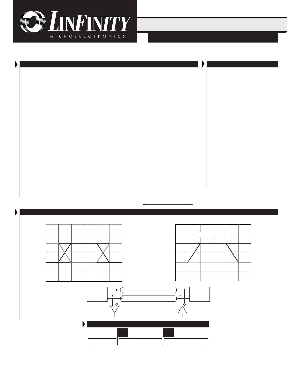
PRODUCT HIGHLIGHT
BUS VOLTAGE V
VOD = V
V
(+)
CM
V
V
(-)
100mV
0V
-100mV
OD
- V
, Logic = 0
(-)
(+)
NEGATED
LX5240 LX5240
PACKAGE ORDER INFO
T
(°C)
A
Plastic SSOP
DB
36-pin
0 to 70 LX5240CDB LX5240CPW
Note: All surface-mount packages are available in Tape & Reel.
Append the letter "T" to part number. (i.e. LX5240CDBT)
Plastic TSSOP
PW
24-pin
Copyright © 1999
Rev. 1.1 10/00
LINFINITY MICROELECTRONICS INC.
11861 WESTERN AVENUE, GARDEN GROVE, CA. 92841, 714-898-8121, FAX: 714-893-2570
1
Page 2
PRODUCT DATABOOK 1996/1997
LX5240
MULTIMODE, PLUG AND PLAY SCSI TERMINATOR
RODUCTION DATA SHEET
P
ABSOLUTE MAXIMUM RATINGS (Note 1)
TermPwr Voltage.................................................................................................+7V
Operating Junction Temperature
Plastic (DB, PW Packages)..........................................................................150°C
Storage Temperature Range..............................................................-65°C to 150°C
Lead Temperature (Soldering, 10 seconds)....................................................300°C
Note 1.Exceeding these ratings could cause damage to the device. All voltages are with
DB PACKAGE:
PW PACKAGE:
Junction Temperature Calculation: TJ = TA + (P
The θ
system. All of the above assume no ambient airflow.
respect to Ground. Currents are positive into, negative out of the specified
terminal.
THERMAL DATA
D
x θ
θθ
θ
θθ
JA
θθ
θ
θθ
JA
).
JA
THERMAL RESISTANCE-JUNCTION TO AMBIENT,
THERMAL RESISTANCE-JUNCTION TO AMBIENT,
numbers are guidelines for the thermal performance of the device/pc-board
JA
MASTER / SLAVE FUNCTION TABLE
MASTER / DIFFSENSE Output
SLAVE Status Current
L* HI Z 0mA
H 1.3V 15mA Source
Open (Pull-up) 1.3V 15mA Source
* When in Low state, terminator will detect state of DIFFSENSE line.
50°C/W
100°C/W
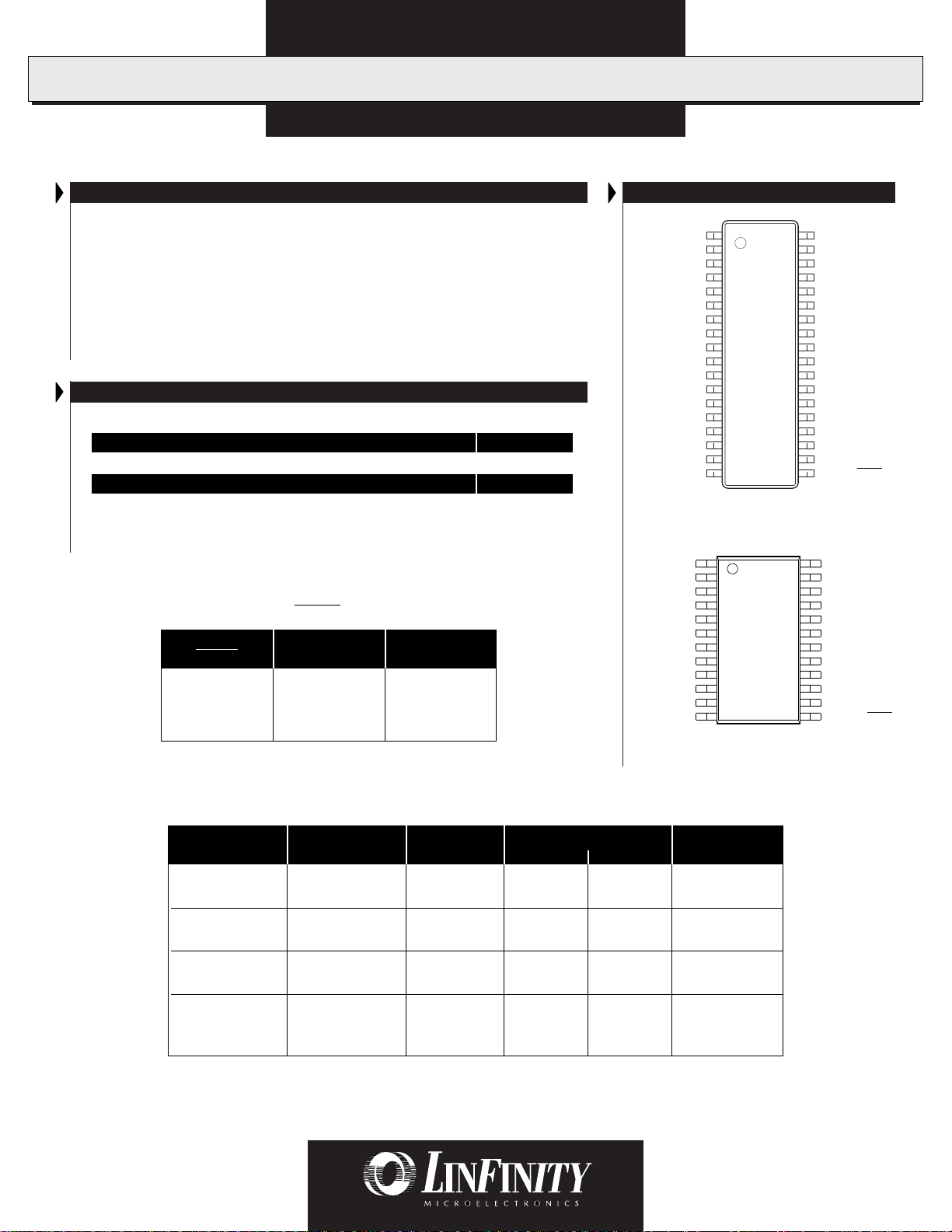
PACKAGE PIN OUTS
136
N.C.
235
N.C.
DISCONNECT A
HEATSINK
HEATSINK
HEATSINK
DISCONNECT B
("N.C." = No Internal Connection)
1+
2+
3+
4+
5+
DISCONNECT B
GND
("N.C." = No Internal Connection)
334
433
1+
532
1-
631
2+
730
2-
829
928
10 27
11 26
3+
12 25
3-
13 24
4+
14 23
4-
15 22
5+
16 21
5-
17 20
18 19
GND
DB PACKAGE (Top View)
1 24
223
1-
322
421
2-
520
619
3-
718
817
4-
916
10 15
5-
11 14
12 13
PW PACKAGE (Top View)
UltraMAX
V
TERM
HVD
LVD
SE
99+
88+
HEATSINK
HEATSINK
HEATSINK
77+
66+
DIFF B
DIFFSENSE
MASTER/SLAVE
V
TERM
DISCONNECT A
99+
88+
77+
66+
DIFFSENSE
MASTER/SLAVE
DIFFSENSE / POWER UP / POWER DOWN FUNCTION TABLE
DISCONNECT ADISCONNECT B
HL
LH
HL
LH
HL
LH
LL
H H X Disable HI Z 10µA
Open Open
2
DIFF Outputs Quiescent
SENSE Status Type Current
L < 0.5V Enable S.E. 7mA
0.7 to 1.9V Enable LVD 21mA
H > 2.4V Disable HI Z 1mA
Copyright © 1999
Rev. 1.1 10/00
Page 3
PRODUCT DATABOOK 1996/1997
UltraMAX
LX5240
MULTIMODE, PLUG AND PLAY SCSI TERMINATOR
PRODUCTION DATA SHEET
RECOMMENDED OPERATING CONDITIONS (Note 2)
Parameter
Termpwr Voltage LVD V
Symbol
TERM
SE
Signal Line Voltage
Disconnect Input Voltage
Operating Virtual Junction Temperature Range
LX5240C
Note 2. Range over which the device is functional.
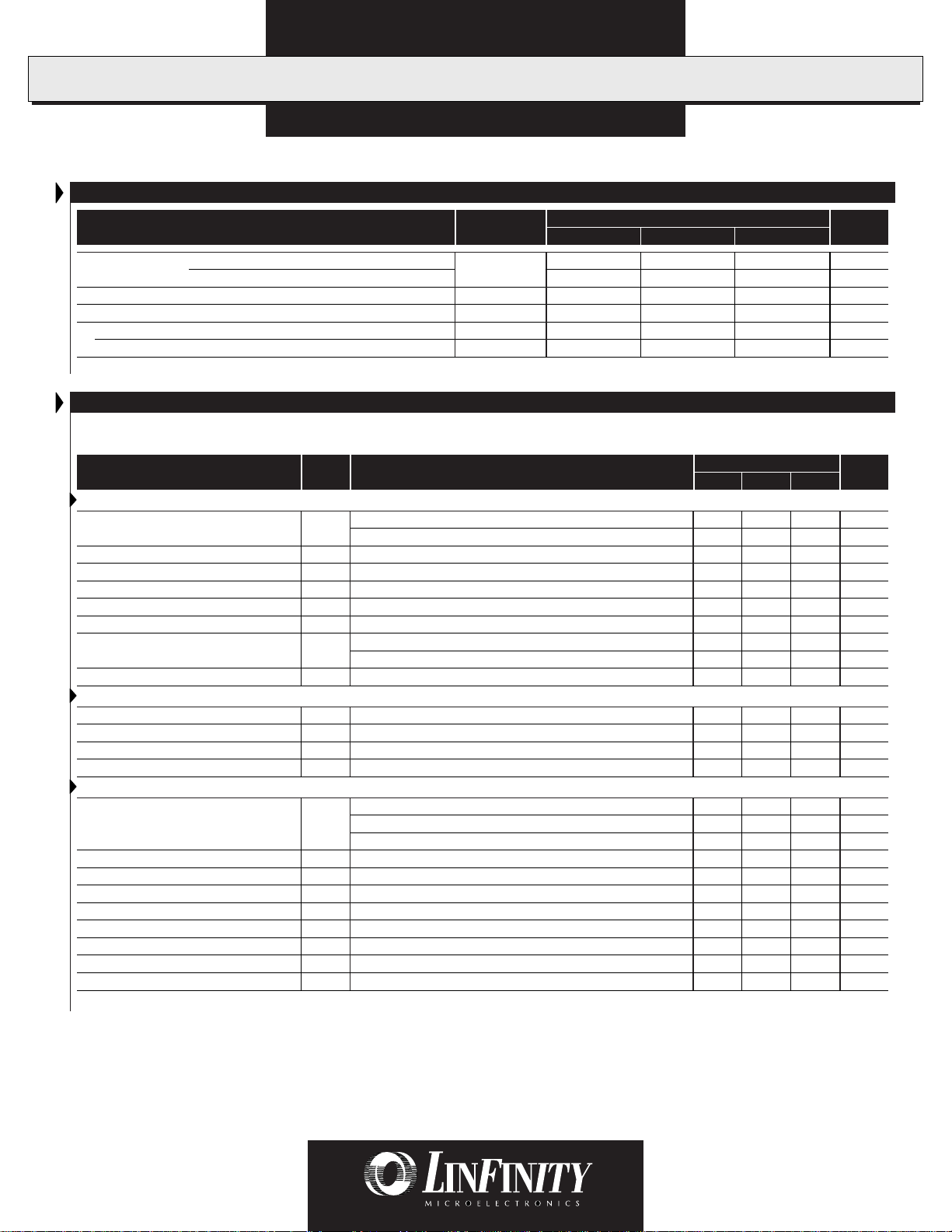
ELECTRICAL CHARACTERISTICS
(Unless otherwise specified, these specifications apply over the operating ambient temperature range of 0°C ≤ TA ≤ 70°C. TermPwr = 4.75V,
DISCONNECT A or B = L. Low duty cycle pulse testing techniques are used which maintains junction and case temperatures equal to the ambient temperature.)
Parameter
Symbol
Test Conditions Units
LVD Terminator Section
TermPwr Supply Current LVD ICCAll term lines = Open
DISCONNECT A or B = LOW
Common Mode Voltage V
Offset Voltage V
Differential Terminator Impedance ZDV
Common Mode Impedance Z
Output Capacitance C
Output Leakage I
Mode Change Delay t
CM
Open circuit between - and + (see Note 3)
FSB
CM
O
LEAK
Differential = -1V to 1V
OUT
0V to 2.5V
DISCONNECT A or B = LOW
DISCONNECT A or B = LOW, V
DISCONNECT A or B = LOW, V
DIFFSENSE = 1.4V to 0V
DF
LINE
TERM
DIFFSENSE Section
DIFFSENSE Output Voltage V
DIFFSENSE Output Source Current I
DIFFSENSE Sink Current I
DIFFSENSE Output Leakage I
DIFF
DIFFVDIFF
SINK(DIFF)VDIFF
LEAK(DIFF)
= 0V
= 2.75V
DISCONNECT A or B = LOW, TA = 25°C
Single-Ended Termination Section
Termpwr Supply Current SE ICCAll term lines = Open, Master/Slave = 0V
All term lines = 0.2V, Master/Slave = 0V
DISCONNECT A or B = LOW
Terminator Output High Volt V
Output Current I
Sink Current I
Output Capacitance C
Leakage Current I
Ground Driver Impedance ZGI = 1mA
Thermal Shutdown
Note 3. Open circuit failsafe voltage.
O
V
O
SINKVOUT
O
LEAK
= 0.2V
OUT
= 4V, All lines
DISCONNECT A or B = LOW
DISCONNECT A or B = LOW, V
DISCONNECT A or B = LOW, V
OUT
TERM
Recommended Operating Conditions
Min. Typ. Max.
3.0 5.25 V
3.5 5.25 V
0 5.0 V
0V
070°C
Min. Typ. Max.
1.125 1.25 1.375 V
100 112 125 mV
100 105 110 Ω
100 200 300 Ω
= 0 to 4V, TA = 25°C
= 0V, V
= 0 to 4V, TA = 25°C
= 0V, V
LINE
LINE
= 2.7V
= 2.7V
TERM
LX5240
25 30 mA
15 35 µA
2.5 pF
2µA
1µA
115 ms
1.2 1.3 1.4 V
5.0 15.0 mA
200 µA
10 µA
710mA
214 226 mA
15 35 µA
2.6 2.85 V
21 23 24 mA
45 65 mA
2.5 pF
2µA
1µA
100 Ω
150 °C
Units
V
Copyright © 1999
Rev. 1.1 10/00
3
Page 4
PRODUCT DATABOOK 1996/1997
LX5240
Parameter
DISCONNECT Section (Plug n' Play)
DISCONNECT A/B Thresholds V
Input Current I
MASTER / SLAVE Section
MASTER / SLAVE Thresholds V
Input Current I
MULTIMODE, PLUG AND PLAY SCSI TERMINATOR
RODUCTION DATA SHEET
P
ELECTRICAL CHARACTERISTICS
Symbol
TH
DISCONNECT A/B = 0V
IL
I
DISCONNECT A/B = 2.4V
IH
TH (MS)
MASTER / SLAVE = 0V
IL (MS)
I
MASTER / SLAVE = 2.4V
IH (MS)
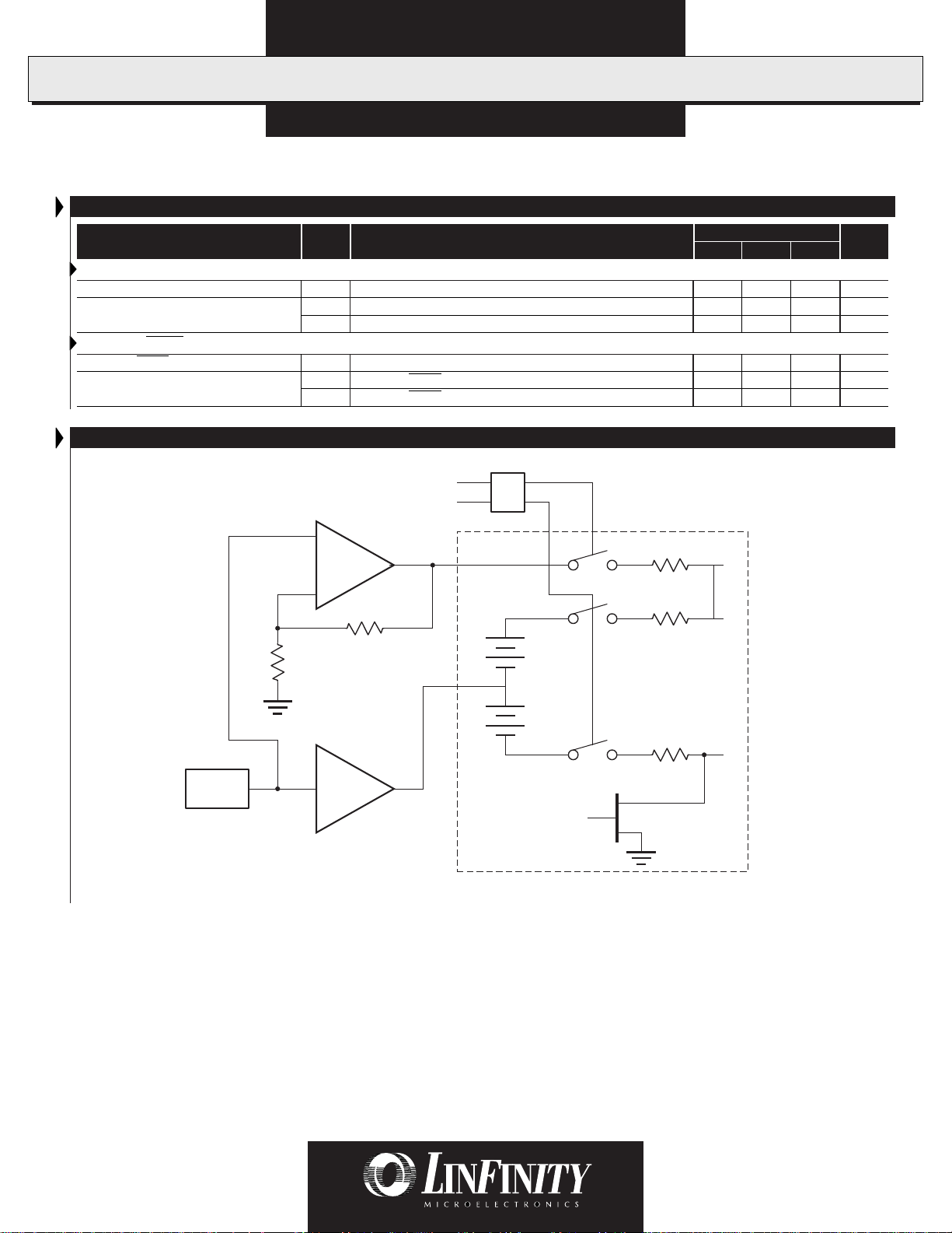
BLOCK DIAGRAM
Test Conditions Units
DISCONNECT
UltraMAX
LX5240
Min. Typ. Max.
0.8 2.0 V
10 µA
100 nA
0.8 2.0 V
10 µA
100 nA
(-)
R
SE
R
LVD
(+)
R
V
BG
LVD
Ground Driver
FIGURE 1 — LX5240 Block Diagram
4
Copyright © 1999
Rev. 1.1 10/00
Page 5
PRODUCT DATABOOK 1996/1997
UltraMAX
5V
2.2µF
Plug n' Play
TERMPWR
Plug n' Play
TERM POWER
DIFFSENSE
V
TERM
LX5240
M/S*
DIFFSENSE
V
TERM
LX5240
MULTIMODE, PLUG AND PLAY SCSI TERMINATOR
PRODUCTION DATA SHEET
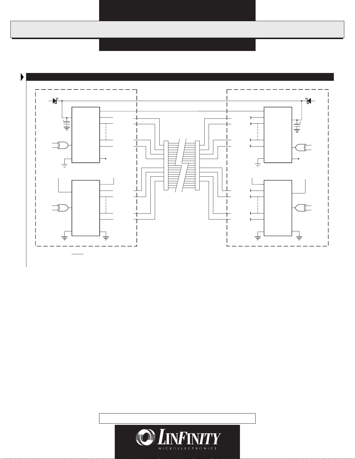
APPLICATION SCHEMATIC
HOST
DIFFSENSE (1.3V)
~
DB (0) -
~
DB (0) +
~
DB (7)-
~
DB (7)+
DIFFSENSE DIFFSENSE
~
ATN -
~
ATN +
~
ACK -
~
ACK +
SCSI CABLE
PERIPHERAL
TERM POWER
DB (0) -
DB (0) +
DB (7)-
DB (7)+
ATN -
ATN +
ACK -
ACK +
DIFFSENSE
V
LX5240
M/S
DIFFSENSE
V
LX5240
LX5240
TERM
TERM
2.2µF
TERMPWR
5V
Plug n' Play
Plug n' Play
M/S
Note: Single-ended the + signals become ground, DIFFSENSE < 0.5V.
* M/S = MASTER/SLAVE
FIGURE 2 — LX5240 Application Schematic
M/S
Copyright © 1999
Rev. 1.1 10/00
PRELIMINARY DATA - Information contained in this document is pre-production data, and is proprietary to LinFinity. It may
not modified in any way without the express written consent of LinFinity. Product referred to herein is offered in sample form
only, and Linfinity reserves the right to change or discontinue this proposed product at any time.
UltraMAX is a trademark of LinFinity Microelectronics Inc.
5
 Loading...