

Page 1
LIN DOC #:
5218
UltraMAX
9-CHANNEL PLUG AND PLAY SCSI TERMINATOR
THE INFINITE POWER OF INNOVATION
DESCRIPTION KEY FEATURES
The LX5218 SCSI terminator is part of Linfinity's
UltraMAX family of high-performance, adaptive, nonlinear mode SCSI products, which are designed to
deliver true UltraSCSI performance in SCSI applications. The low voltage BiCMOS architecture employed in their design offers superior performance
to older linear passive and active techniques.
Linfinity's UltraMAX architecture employs high-speed
adaptive elements for each channel, thereby providing
the fastest response possible — typically 35MHz,
which is 100 times faster than the older linear regulator/terminator approach used by other manufacturers. Products using this older linear regulator approach have bandwidths which are dominated by the
output capacitor and which are limited to 500KHz
(see further discussion in the Functional Description
section). The UltraMAX architecture also eliminates
the output compensation capacitor typical in earlier
terminator designs. It is approved for use with SCSI1, -2, -3, UltraSCSI and beyond — providing the
highest performance alternative available today.
Another key improvement offered by the LX5218
lies in its ability to insure reliable, error free communications even in systems which do not adhere
to recommended SCSI hardware design guidelines,
such as the use of improper cable lengths and
IMPORTANT: For the most current data, consult LinFinity's web site: http://www.linfinity.com.
impedances. Frequently, this situation is not controlled by the peripheral or host designer and, when
problems occur, they are the first to be made aware
of the problem. The LX5218 architecture is much
more tolerant of marginal system integrations.
The LX5218 has two disconnect pins for SCSI Plug
and Play (PnP) applications. Quiescent current is
typically less than (275µA) in disable mode, while
the output capacitance is also less than 3pF. The
obvious advantage of extended battery life for
portable systems is inherent in the product's sleepmode feature. Additionally, the disable function
permits factory-floor or production-line
configurability, reducing inventory and product-line
diversity costs. Field configurability can also be
accomplished without physically removing components which, often times results in field returns due
to mishandling.
Reduced component counts is also inherent in
the LX5218 architecture. Traditional termination
techniques require large stabilization and transient
protection capacitors of up to 20µF in value and
size. The LX5218 architecture does not require these
components, allowing all the cost savings associated
with inventory, board space, assembly, reliability,
and component costs.
P RODUCTION DATA SHEET
TM
LX5218
■ SCSI PLUG AND PLAY, DUAL LOW
DISCONNECT, LOGIC LOW COMMAND
DISCONNECTS ALL TERMINATION LINES
■ HOT SWAP COMPATIBLE
■ ULTRA-FAST RESPONSE FOR FAST-20
SCSI APPLICATIONS
■ 35MHz CHANNEL BANDWIDTH
■ 3.5V OPERATION
■ LESS THAN 3pF OUTPUT CAPACITANCE
■ DISABLE-MODE CURRENT LESS THAN
275µA
■ THERMALLY SELF LIMITING
NO EXTERNAL COMPENSATION
■
CAPACITORS
WIDE
■ IMPLEMENTS 8-BIT OR 16-BIT (
APPLICATIONS
■ COMPATIBLE WITH ACTIVE NEGATION
DRIVERS (60mA / CHANNEL)
■ COMPATIBLE WITH PASSIVE AND
ACTIVE TERMINATIONS
■ APPROVED FOR USE WITH SCSI-1, -2, -3
AND ULTRASCSI
■ CONSULT FACTORY FOR APPLICATION
TEST REPORT
)
PRODUCT HIGHLIGHT
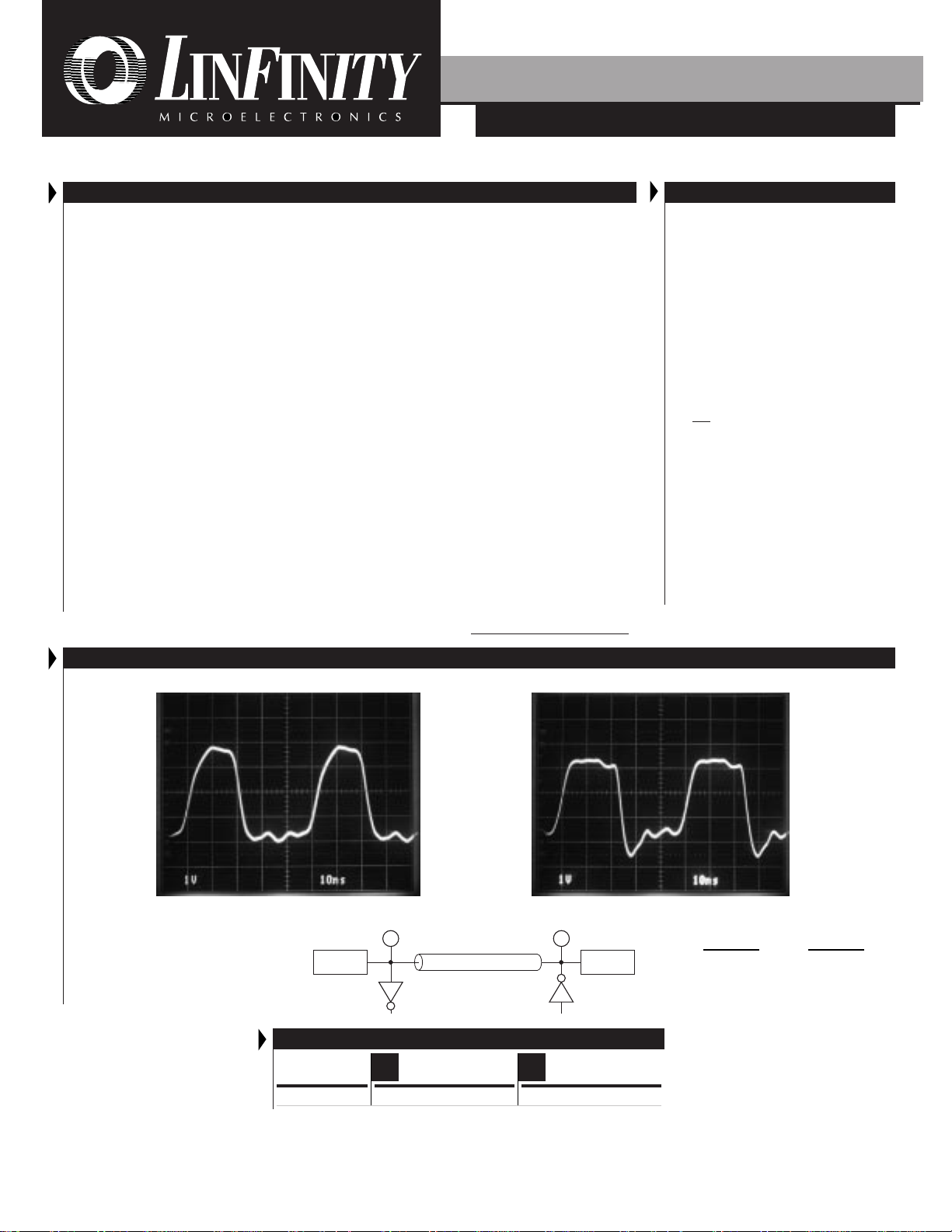
DRIVING WAVEFORM - 20MHZRECEIVING WAVEFORM - 20MHZ
Receiver
1 Meter, AWG 28
LX5218 LX5218
LX5268 LX5268
PACKAGE ORDER INFORMATION
T
(°C)
J
Plastic SOWB
DW PW
16-pin
0 to 70 LX5218CDW LX5218CPW
Note: All surface-mount packages are available in Tape & Reel.
Append the letter "T" to part number. (i.e. LX5218CDWT)
Driver
Plastic TSSOP
20-pin
NOTE:
For An In-Depth
Discussion On Applying
SCSI, Request Linfinity
Application Note:
"Understanding The
Single-Ended SCSI Bus"
Copyright © 1997
Rev. 1.7 12/97
L INFINITY MICROELECTRONICS INC.
11861 WESTERN AVENUE, GARDEN GROVE, CA. 92841, 714-898-8121, FAX: 714-893-2570
1
Page 2
PRODUCT DATABOOK 1996/1997
LX5218
9-CHANNEL PLUG AND PLAY SCSI TERMINATOR
RODUCTION DATA SHEET
P
ABSOLUTE MAXIMUM RATINGS (Note 1)
Continuous Termination Voltage .......................................................................... 10V
Continuous Output Voltage Range .............................................................. 0 to 5.5V
Continuous Disable Voltage Range ............................................................. 0 to 5.5V
Operating Junction Temperature ........................................................... 0°C to 125°C
Storage Temperature Range ............................................................. -65°C to +150°C
Solder Temperature (Soldering, 10 seconds) ................................................... 300°C
Note 1. Exceeding these ratings could cause damage to the device.
THERMAL DATA
DW PACKAGE:
D
x θ
θθ
θ
θθ
JA
θθ
θ
θθ
JA
).
JA
THERMAL RESISTANCE-JUNCTION TO AMBIENT,
PW PACKAGE:
THERMAL RESISTANCE-JUNCTION TO AMBIENT,
Junction Temperature Calculation: TJ = TA + (P
numbers are guidelines for the thermal performance of the device/pc-board system.
The θ
JA
All of the above assume no ambient airflow.
95°C/W
144°C/W
UltraMAX
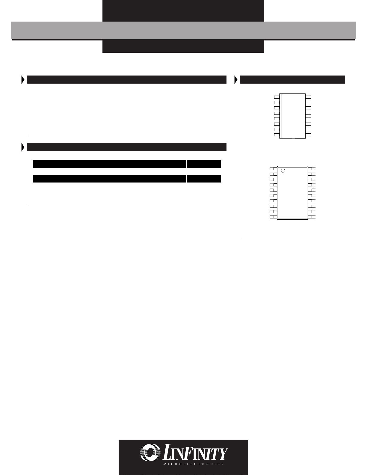
PACKAGE PIN OUTS
TERM POWER
GND
TERM POWER
N.C.
N.C.
D0
D1
D2
D3
D4
N.C.
GND
1 16
215
N.C.
314
D0
413
D1
512
D2
611
D3
710
D4
89
DW PACKAGE
(Top View)
219
318
417
516
615
714
813
912
10 11
20
TERM POWER
DISC1
DISC2
D8
D7
D6
D5
GND
TERM POWER
DISC1
DISC2
D8
D7
N.C.
D6
D5
N.C.
GND
PW PACKAGE
(Top View)
2
Copyright © 1997
Rev. 1.7 12/97
Page 3
PRODUCT DATABOOK 1996/1997
UltraMAX
LX5218
9-CHANNEL PLUG AND PLAY SCSI TERMINATOR
P RODUCTION DATA SHEET
RECOMMENDED OPERATING CONDITIONS (Note 2)
Parameter
Termination Voltage V
High Level Disable Input Voltage V
Low Level Disable Input Voltage V
Operating Virtual Junction Temperature Range
LX5218C
Note 2. Range over which the device is functional.
Symbol
TERM
IH
IL
ELECTRICAL CHARACTERISTICS
Term Power = 4.75V unless otherwise specified. Unless otherwise specified, these specifications apply at the recommended operating ambient temperature of T
= 25°C. Low duty cycle pulse testing techniques are used which maintains junction and case temperatures equal to the ambient temperature.
A
Parameter
Output High Voltage V
TermPwr Supply Current I
Output Current I
Disable Input Current I
Output Leakage Current I
Capacitance in Disabled Mode C
Channel Bandwidth BW
Termination Sink Current, per Channel I
Symbol
OUT
CC
OUTVOUT
IN
OL
OUTVOUT
SINKVOUT
Test Conditions Units
All data lines = open
All data lines = 0.5V
DISC1 Pin = DISC2 Pin = 0V
= 0.5V
DISC1 Pin = DISC2 Pin = 4.75V
DISC1 Pin = DISC2 Pin = 0V
DISC1 Pin = DISC2 Pin = 0V, VO = 0.5V
= 0V, frequency = 1MHz
= 4V
Recommended Operating Conditions
Min. Typ. Max.
3.5 5.5 V
2V
0 0.8 V
0 125 °C
TERM
LX5218
Min. Typ. Max.
2.65 2.85 V
69mA
215 225 mA
275 µA
-21 -23 -24 mA
90 µA
-10 nA
10 nA
3pF
35 MHz
60 mA
Units
V
Copyright © 1997
Rev. 1.7 12/97
3
Page 4
PRODUCT DATABOOK 1996/1997
T
LX5218
DISC1
DISC2
TERM POWER
THERMAL
LIMITING
CIRCUIT
9-CHANNEL PLUG AND PLAY SCSI TERMINATOR
RODUCTION DATA SHEET
P
BLOCK DIAGRAM
CURRENT
BIASING
CIRCUIT
24mA CURRENT
LIMITING CIRCUIT
2.85V
UltraMAX
DATA OUTPU
PIN DB(0)
1 OF 9 CHANNELS
FUNCTIONAL DESCRIPTION
Cable transmission theory suggests to optimize signal speed
and quality, the termination should act both as an ideal voltage
reference when the line is released (deasserted) and as an
ideal current source when the line is active (asserted).
Common active terminators,
which consist of Linear Regulators
in series with resistors (typically
110Ω), are a compromise. As the
line voltage increases, the amount
of current decreases linearly by the
equation V = I * R. The LX5218,
with its unique new architecture
applies the maximum amount of
current regardless of line voltage
until the termination high threshold (2.85V) is reached.
Acting as a near ideal line terminator, the LX5218 closely reproduces the optimum case
when the device is enabled. To enable the device the DISC1
and DISC2 Pins must be pulled logic High, Open, or any
combination of both High and Low. During this mode of
operation, quiescent current is 6mA and the device will
POWER UP / POWER DOWN FUNCTION TABLE
DISC1 DISC2
H H Enabled 6mA
H L Enabled 6mA
L H Enabled 6mA
L L Disabled 275µA
Open Open Enabled 6mA
respond to line demands by delivering 24mA on assertion and
by imposing 2.85V on deassertion. In order to disable the
device, the DISC1 and DISC2 pins must be driven logic Low.
This mode of operation places the device in a sleep state where
a meager 275µA of quiescent current is consumed. Additionally, all
outputs are in a Hi-Z (impedance)
Outputs
LX5218 has been optimized to have only 3pF of capacitance
per output in the sleep state.
An additional feature of the LX5218 is its compatibility with
active negation drivers. The device handles up to 60mA of
sink current for drivers which exceed the 2.85V output high.
Quiescent
Current
state. Sleep mode can be used for
power conservation or to completely eliminate the terminator
from the SCSI chain. In the second
case, termination node capacitance
is important to consider. The ter-
minator will appear as a parasitic
distributed capacitance on the line,
which can detract from bus performance. For this reason, the
4
Copyright © 1997
Rev. 1.7 12/97
Page 5

PRODUCT DATABOOK 1996/1997
UltraMAX
9-CHANNEL PLUG AND PLAY SCSI TERMINATOR
P RODUCTION DATA SHEET
GRAPH / CURVE INDEX
Waveforms
FIGURE #
1A. RECEIVING WAVEFORM (Freq. = 1.0MHz)
1B. DRIVING WAVEFORM
2A. RECEIVING WAVEFORM (Freq. = 5.0MHz)
2B. DRIVING WAVEFORM
3. 10MHz WAVEFORM
4. 20MHz WAVEFORM
Characteristic Curves
FIGURE #
5. OUTPUT HIGH VOLTAGE vs. JUNCTION TEMPERATURE
6. OUTPUT CURRENT vs. JUNCTION TEMPERATURE
7. OUTPUT CURRENT vs. OUTPUT HIGH VOLTAGE (V
8. OUTPUT CURRENT vs. OUTPUT HIGH VOLTAGE (VT = 3.3V)
9. TERMINATION VOLTAGE vs. SUPPLY CURRENT
10. TERMPWR SUPPLY CURRENT vs. TERMINATION VOLTAGE (Disabled)
— LX5218
11. OUTPUT HIGH VOLTAGE vs. JUNCTION TEMPERATURE (V
12. OUTPUT CURRENT vs. JUCTION TEMPERATURE (VT = 3.3V)
13. OUTPUT HIGH VOLTAGE vs. TERMINATION VOLTAGE
14. OUTPUT CURRENT vs. TERMINATION VOLTAGE
15. OUTPUT CURRENT MATCHING CHANNEL TO CHANNEL
= 4.75V)
T
= 3.3V)
T
LX5218
FIGURE INDEX
Application Circuits
FIGURE #
16. 8-BIT SCSI SYSTEM APPLICATION
Copyright © 1997
Rev. 1.7 12/97
5
Page 6

PRODUCT DATABOOK 1996/1997
)
LX5218
FIGURE 1A. —
3.5
3
2.5
2
1.5
1
Line Voltage - (V)
0.5
9-CHANNEL PLUG AND PLAY SCSI TERMINATOR
RODUCTION DATA SHEET
P
CHARACTERISTIC CURVES
RECEIVING WAVEFORM FIGURE 1B. — DRIVING WAVEFORM
3.5
freq.=1.03844MHz
Line Voltage - (V)
freq.=1.00266MHz
3
2.5
2
1.5
1
0.5
UltraMAX
GND
-0.5
Time - (250ns/Div.)
Fig. 1A
LX5218 LX5218
END-DRIVEN CABLE
Receiver
6 Meter, 92
75C08 75C08
GND
-0.5
Time - (250ns/Div.
Driver
Fig. 1B
W
6
Copyright © 1997
Rev. 1.7 12/97
Page 7

PRODUCT DATABOOK 1996/1997
)
)
UltraMAX
FIGURE 2A. —
3.5
freq.=5.0092MHz
3
2.5
2
1.5
1
Line Voltage - (V)
0.5
LX5218
9-CHANNEL PLUG AND PLAY SCSI TERMINATOR
P RODUCTION DATA SHEET
CHARACTERISTIC CURVES
RECEIVING WAVEFORM FIGURE 2B. — DRIVING WAVEFORM
3.5
freq.=4.9961MHz
3
2.5
2
1.5
1
Line Voltage - (V)
0.5
GND
-0.5
GND
-0.5
Time - (50ns/Div.
END-DRIVEN CABLE
Receiver
Driver
Fig. 2A
6 Meter, 92
W
LX5218 LX5218
75C08 75C08
Time - (50ns/Div.
Fig. 2B
Copyright © 1997
Rev. 1.7 12/97
7
Page 8

PRODUCT DATABOOK 1996/1997
)
)
LX5218
FIGURE 3. —
4
3
2
1
0
4
Line Voltage - (V)
9-CHANNEL PLUG AND PLAY SCSI TERMINATOR
RODUCTION DATA SHEET
P
CHARACTERISTIC CURVES
10MHz WAVEFORM FIGURE 4. — 20MHz WAVEFORM
4
Ch2 Freq.=10.096MHz
#2
#1
#3
Line Voltage - (V)
Ch2 Freq.=20.020MHz
3
2
1
0
4
#1
UltraMAX
#2
#3
GND
GND
Time - (20ns/Div.
END-DRIVEN CABLE
4.75V 4.75V
12
6 Meter, 72
W
LX5218 LX5218
LX5268
3
LX5268
Time - (10ns/Div.
8
Copyright © 1997
Rev. 1.7 12/97
Page 9

PRODUCT DATABOOK 1996/1997
0
15
(TJ) Junction Temperature - (°C)
(I
OUT
) Output Current - (mA)
20
5025 75 100
25
10
5
30
125
VT = 4.75V
UltraMAX
FIGURE 5. —
4.5
4
3.5
3
) Output High Voltage - (V)
2.5
OUT
(V
LX5218
9-CHANNEL PLUG AND PLAY SCSI TERMINATOR
P RODUCTION DATA SHEET
CHARACTERISTIC CURVES
OUTPUT HIGH VOLTAGE vs. JUNCTION TEMP. FIGURE 6. — OUTPUT CURRENT vs. JUNCTION TEMP.
2
0
FIGURE 7. — OUTPUT CURRENT vs. OUTPUT HIGH VOLTAGE FIGURE 8. — OUTPUT CURRENT vs. OUTPUT HIGH VOLTAGE
20
15
10
) Output Current - (mA)
OUT
(I
5
0
00.8
5025 75 100
(TJ) Junction Temperature - (°C)
0.4
(V
) Output High Voltage - (V)
OUT
1.61.2 2 2.4
VT = 4.75V
= 25°C
T
A
2.8253.2
125
20
15
10
) Output Current - (mA)
OUT
(I
5
0
0.4
00.8
(V
) Output High Voltage - (V)
OUT
VT = 3.3V
T
1.61.2 2 2.4
= 25°C
A
2.8253.2
Copyright © 1997
Rev. 1.7 12/97
9
Page 10

PRODUCT DATABOOK 1996/1997
LX5218
FIGURE 9. —
7
6
5
4
3
2
) TermPwr Supply Current - (mA)
CC
1
(I
9-CHANNEL PLUG AND PLAY SCSI TERMINATOR
TERMPWR SUPPLY CURRENT
vs. TERMINATION VOLTAGE
RODUCTION DATA SHEET
P
CHARACTERISTIC CURVES
FIGURE 10. — LX5218 TERMPWR SUPPLY CURRENT
400
350
300
250
200
150
100
) TermPwr Supply Current - (µA)
CC
50
(I
UltraMAX
vs. TERMINATION VOLTAGE (Disabled)
0
2.5
3
(V
TERM
3.5
4.5455.5
) Termination Voltage - (V)
6
0
0
(V
1
2
) Termination Voltage - (V)
TERM
435
FIGURE 11. — OUTPUT HIGH VOLTAGE vs. JUNCTION TEMP. FIGURE 12. — OUTPUT CURRENT vs. JUNCTION TEMP.
4.5
VT = 3.3V
4
3.5
3
) Output High Voltage - (V)
2.5
OUT
30
VT = 3.3V
25
20
15
) Output Current - (mA)
OUT
(I
10
(V
2
0
5025 75 100
125
5
0
5025 75 100
6
125
10
(TJ) Junction Temperature - (°C)
(TJ) Junction Temperature - (°C)
Copyright © 1997
Rev. 1.7 12/97
Page 11

PRODUCT DATABOOK 1996/1997
UltraMAX
FIGURE 13. —
4
3.5
3
2.5
2
1.5
) Output High Voltage - (V)
1
OUT
(V
0.5
9-CHANNEL PLUG AND PLAY SCSI TERMINATOR
OUTPUT HIGH VOLTAGE
vs. TERMINATION VOLTAGE
P RODUCTION DATA SHEET
CHARACTERISTIC CURVES
FIGURE 14. — OUTPUT CURRENT vs. TERMINATION VOLTAGE
25
20
15
10
) Output High Voltage - (V)
5
OUT
(V
LX5218
0
3
3.5 4
(V
) Termination Voltage - (V)
TERM
4.5
55.56
0
3
3.5 4
(V
) Termination Voltage - (V)
TERM
4.5
55.56
Copyright © 1997
Rev. 1.7 12/97
11
Page 12

PRODUCT DATABOOK 1996/1997
LX5218
24
23.5
23
22.5
Io (mA)
22
21.5
21
UltraMAX
9-CHANNEL PLUG AND PLAY SCSI TERMINATOR
RODUCTION DATA SHEET
P
CHARACTERISTIC CURVES
FIGURE 15. —
1
2
3
4
5
6
7
OUTPUT CURRENT CHANNEL TO CHANNEL MATCHING
8
9
10
11
12
13
14
15
16
17
18
19
Part #
20
21
22
23
23.5 - 24
23 - 23.5
22.5 - 23
22 - 22.5
21.5 - 22
21 - 21.5
i8
i6
i4
Channel
i2
i0
24
25
5V
2.2µF
DISC1
DISC2
TERMPWR
DISC1
DISC2
Note: Add third LX5218 for 16-bit SCSI
TERM POWER
V
TERM
LX5218
V
TERM
PRODUCTION DATA - Information contained in this document is proprietary to Linfinity, and is current as of publication date. This document
may not be modified in any way without the express written consent of Linfinity. Product processing does not necessarily include testing of
all parameters. Linfinity reserves the right to change the configuration and performance of the product and to discontinue product at any time.
TERMPWR TERMPWR
APPLICATION SCHEMATIC
FIGURE 16 — 8-BIT SCSI SYSTEM APPLICATION
~
DB (0)
~
DB (1)
~
DB (6)
~
DB (7)
~
DB (P)
~
ATN
~
BSY
~
ACK
~
RST
~
MSG
HOST
SCSI CABLE
TM
UltraMAX is a trademark of Linfinity Microelectronics Inc.
PERIPHERAL
DB (0)
DB (1)
DB (6)
DB (7)
DB (P)
ATN
BSY
ACK
RST
MSG
TERM POWER
V
TERM
LX5218
V
TERM
LX5218LX5218
5V
2.2µF
DISC1
DISC2
TERMPWR
DISC1
DISC2
12
Copyright © 1997
Rev. 1.7 12/97
 Loading...