

Page 1
LIN DOC #:
LX5207
18-LINE LOW CAPACITANCE, µPOWER SCSI TERMINATOR
5207
THE INFINITE POWER OF INNOVATION
DESCRIPTION
The LX5207 is an eighteen line active terminator for the SCSI parallel bus. This SCSI
standard recommends active termination at
both ends of the SCSI bus.
During disconnect mode, the LX5207
requires a meager 500nA of supply current
while offering only 2.5pF of output capacitance. To enter this low power mode, the
disconnect pin can be left open (floating)
or driven high thereby disconnecting the
terminating resistors and placing the internal low dropout regulator into low power
mode. In disconnect mode each termination line presents a high impedance to the
SCSI bus with the overall effect being to
preserve high signal integrity and subsequent reliable, error free communications.
During normal operation, the LX5207
consumes only 800µA of current which is
the lowest enabled supply current of any
terminator available on the market today.
Linfinity's proprietary BiCMOS low dropout
regulator architecture enables this unique
and very efficient operating characteristic.
The LX5207 also offers a precisely
trimmed channel output current specified
to a 5% tolerance. The maximum value
of the output current is trimmed as closely
as possible to the SCSI standard maximum
specification to give the highest possible
noise margin for fast SCSI operation. And
finally, the LX5207 sinks up to 100mA of
current making it compatible with today's
fast active negation drivers.
The LX5207 is a superior, pin-for-pin
replacement for a variety of industry products such as the UC5601, UC5602, UC5608,
and UC5609.
PRODUCT HIGHLIGHT
P RODUCTION DATA SHEET
KEY FEATURES
■ 2.5pF OUTPUT CAPACITANCE DURING
DISCONNECT
■ 500nA SUPPLY CURRENT IN DISCONNECT
MODE
■ 800µA SUPPLY CURRENT DURING NORMAL
OPERATION
■ 100mA SINK CURRENT FOR ACTIVE
NEGATION
■ LOGIC COMMAND DISCONNECTS ALL
TERMINATION LINES
■ CURRENT LIMIT AND THERMAL PROTEC-
TION
■ COMPATIBLE WITH SCSI 1, 2, 3, AND
FAST-20 STANDARDS
■ HOT SWAP COMPATIBLE
■ CONSULT FACTORY FOR APPLICATION
TEST REPORT: 5207TR
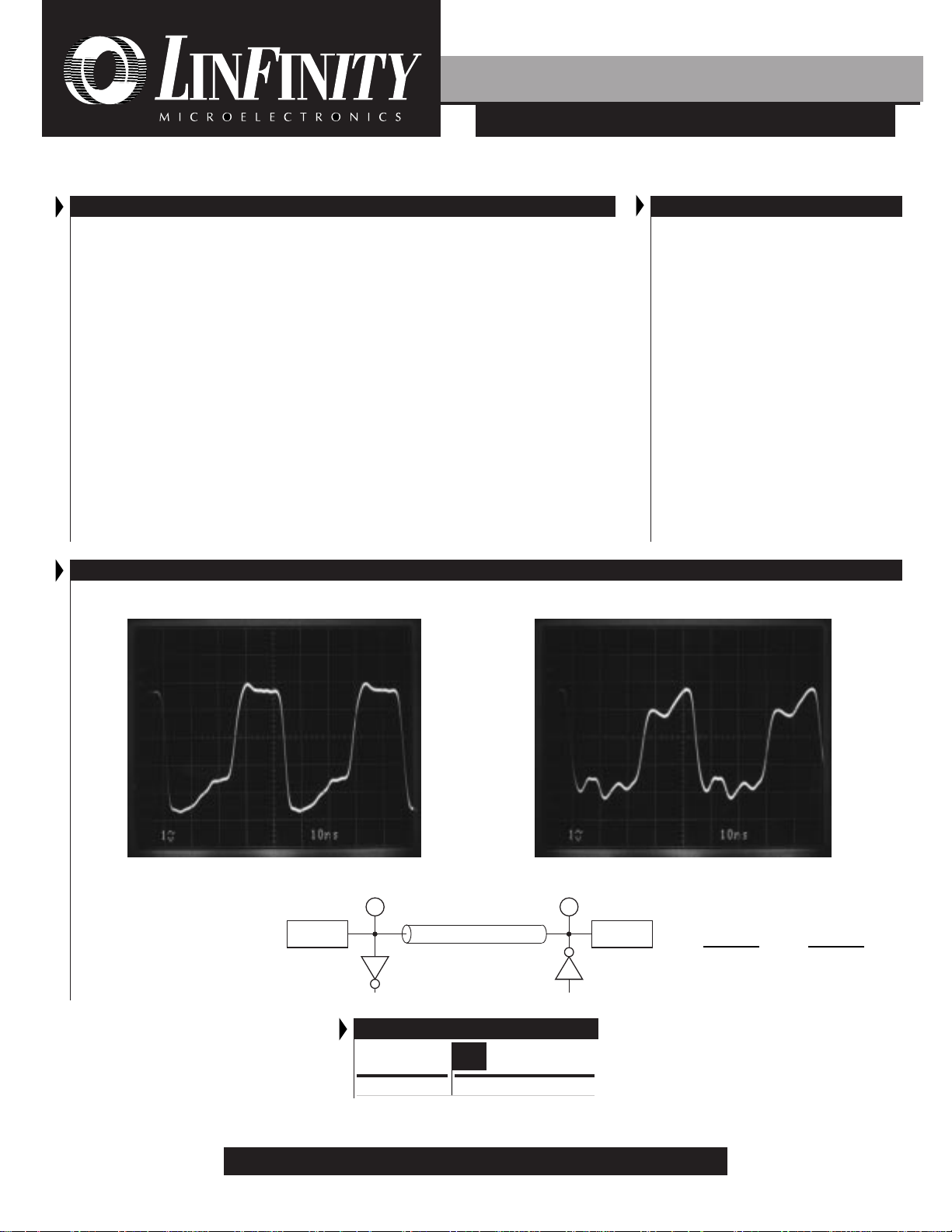
RECEIVING WAVEFORM - 20MHZ DRIVING WAVEFORM - 20MHZ
Receiver
Driver
1 Meter, AWG 28
LX5207 LX5207
LX5268 LX5268
Discussion On Applying
NOTE:
For An In-Depth
SCSI, Request Linfinity
PACKAGE ORDER INFO
T
(°C)
A
0 to 70 LX5207CDWP
Note: All surface-mount packages are available in Tape & Reel.
Append the letter "T" to part number. (i.e. LX5207CDWPT)
Plastic SOWB
DWP
28-pin, Power
Application Note:
"Understanding The
Single-Ended SCSI Bus"
Copyright © 1998
Rev. 1.5 3/98
FOR FURTHER INFORMATION CALL (714) 898-8121
11861 WESTERN AVENUE, GARDEN GROVE, CA. 92841
1
Page 2
LX5207
PRODUCT DATABOOK 1996/1997
18-LINE LOW CAPACITANCE, µPOWER SCSI TERMINATOR
RODUCTION DATA SHEET
P
ABSOLUTE MAXIMUM RATINGS (Note 1)
TermPwr Voltage .................................................................................................+7V
Signal Line Voltage ................................................................................... 0V to +7V
Regulator Output Current ................................................................................... 1.2A
Operating Junction Temperature
Plastic (DWP Package)................................................................................. 150°C
Storage Temperature Range .............................................................. -65°C to 150°C
Lead Temperature (Soldering, 10 seconds) .................................................... 300°C
Note 1. Exceeding these ratings could cause damage to the device. All voltages are with
respect to Ground. Currents are positive into, negative out of the specified
terminal.
THERMAL DATA
DWP PACKAGE:
D
θθ
θ
θθ
JL
x θ
θθ
θ
θθ
JA
).
JA
THERMAL RESISTANCE-JUNCTION TO LEADS,
THERMAL RESISTANCE-JUNCTION TO AMBIENT,
Junction Temperature Calculation: T
numbers are guidelines for the thermal performance of the device/pc-board
The θ
JA
system. All of the above assume no ambient airflow.
= TA + (P
J
18°C/W
40°C/W
POWER UP / POWER DOWN FUNCTION TABLE
Disconnect Outputs
L Enabled 800µA
H HI Z 0.5µA
Open HI Z 0.5µA
Quiescent
Current
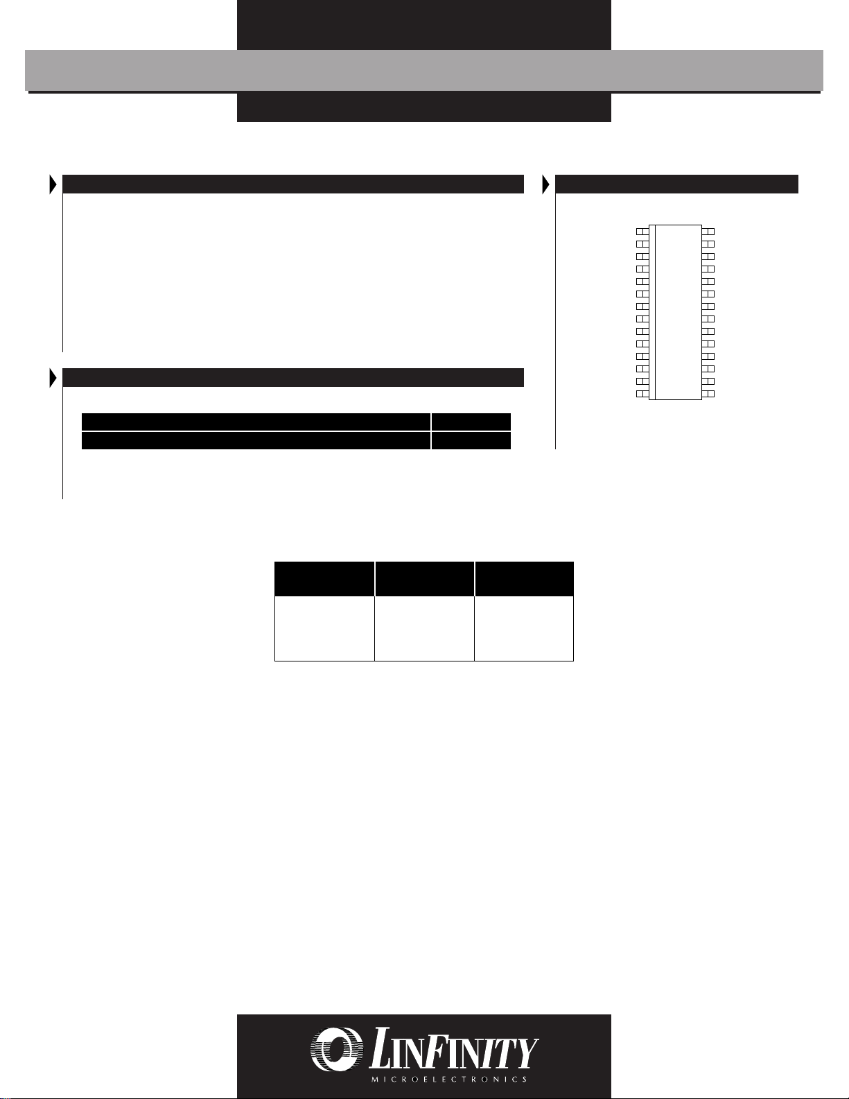
PACKAGE PIN OUTS
DISCONNECT
HEAT SINK
HEAT SINK
HEAT SINK
V
128
T1
227
T2
326
T3
425
T4
524
T5
623
722
821
920
T6
10 19
T7
11 18
T8
12 17
T9
13 16
14 15
TERM
DWP PACKAGE
(Top View)
GND
T18
T17
T16
T15
T14
HEAT SINK
HEAT SINK
HEAT SINK
T13
T12
T11
T10
REG OUT
2
Copyright © 1998
Rev. 1.5 3/98
Page 3

PRODUCT DATABOOK 1996/1997
LX5207
18-LINE LOW CAPACITANCE, µPOWER SCSI TERMINATOR
P RODUCTION DATA SHEET
RECOMMENDED OPERATING CONDITIONS (Note 2)
Parameter
Termpwr Voltage V
Symbol
TERM
Signal Line Voltage
Disconnect Input Voltage
Output Capacitance on REGOUT
Operating Virtual Junction Temperature Range
LX5207C
Note 2. Range over which the device is functional.
ELECTRICAL CHARACTERISTICS
(Unless otherwise specified, these specifications apply over the operating ambient temperature range of 0°C ≤ TA ≤ 70°C. Termpwr = 4.75V, Disconnect
= 0V. Low duty cycle pulse testing techniques are used which maintains junction and case temperatures equal to the ambient temperature.)
Parameter
Symbol
Test Conditions Units
Supply Current Section
Termpwr Supply Current All term lines = Open
All term lines = 0.5V
Power Down Mode Disconnect = Open
Output Section (Terminator Lines)
Terminator Impedance I
Terminator Output High Voltage
Max. Output Current V
Output Leakage Disconnect = Open, V
Output Capacitance Disconnect = Open
Sink Current V
= -5mA to -15mA
TERM
= 0.5V, TA = 25°C
OUT
= 0.5V, 0°C ≤ TA ≤ 70°C
V
OUT
V
OUT
V
OUT
OUT
= 0.5V, V
= 0.5V, V
= 4V
= 4V, TA = 25°C
TERM
= 4V, 0°C ≤ TA ≤ 70°C
TERM
= 0V to 5.25V
TERM
Regulator Section
Regulator Output Voltage
Line Regulation V
Load Regulation I
Drop Out Voltage I
Short Circuit Current V
= 4V to 6V
TERM
= 0 to -100mA
REG
= -100mA
REG
= 0V
REG
Thermal Shutdown
Disconnect Section
Disconnect Threshold
Input Current Disconnect = 0V
Recommended Operating Conditions
Min. Typ. Max.
Units
4 5.25 V
05V
0V
TERM
V
4.7 µF
070°C
LX5207
Min. Typ. Max.
0.8 2.0 mA
390 415 mA
0.5 1 µA
100 110 120 Ω
2.7 2.9 V
-20.3 -21.8 -23 mA
-19.0 -21.8 -23 mA
-19.5 -21.8 -23 mA
-18.0 -21.8 -23 mA
10 400 nA
2.5 pF
58 70 mA
3.6 V
10 20 mV
20 50 mV
0.45 1.0 V
-800 -1100 mA
150 °C
0.8 2.0 V
40 µA
Copyright © 1998
Rev. 1.5 3/98
3
Page 4

LX5207
DISCONNECT
PRODUCT DATABOOK 1996/1997
18-LINE LOW CAPACITANCE, µPOWER SCSI TERMINATOR
RODUCTION DATA SHEET
P
BLOCK DIAGRAM
FIGURE 1 — LX5207 BLOCK DIAGRAM
REG OUT
V
TERM
V
TERM
Channel
1 of 18
5V
4.7µF
DISCONNECT
4.7µF
TERM POWER
V
TERM
LX5207
REGOUT
VBG
APPLICATION SCHEMATIC
FIGURE 2 — 8/16-BIT SCSI SYSTEM APPLICATION
Narrow
~
DB (0)
~
DB (1)
~
DB (14)
~
DB (15)
~
DB (P1)
HOST
PERIPHERAL
Narrow
DB (0)
DB (1)
DB (14)
DB (15)
DB (P1)
V
TERM
TERM POWER
V
TERM
LX5207
REGOUT
T0
T17
4.7µF
4.7µF
5V
DISCONNECTDISCONNECT
V
TERM
TERMPWR
2.2µF
Copyright © 1998
Rev. 1.5 3/98
TERMPWR
DISCONNECT
2.2µF
V
TERM
LX5212
REGOUT
PRODUCTION DATA - Information contained in this document is proprietary to LinFinity, and is current as of publication date. This document
may not be modified in any way without the express written consent of LinFinity. Product processing does not necessarily include testing of
all parameters. Linfinity reserves the right to change the configuration and performance of the product and to discontinue product at any time.
Wide
~
MSG
~
RST
~
ACK
~
BSY
~
ATN
SCSI CABLE
Wide
MSG
RST
ACK
BSY
ATN
LX5212
REGOUT
4
 Loading...