

Page 1
LIN DOC #:
5122
UltraMAX
ULTRA 27-LINE, PLUG AND PLAY SCSI TERMINATOR
T HE I NFINITE P OWER OF I NNOVATION
DESCRIPTION KEY FEATURES
The LX5122 Plug and Play UltraMAXTM terminator represents next-generation technology for SCSI termination applications. The
low-voltage BiCMOS architecture employed
in its design offers superior performance to
older passive and active techniques.
Linfinity's architecture employs highspeed adaptive elements for each channel,
providing the fastest response possible. The
channel bandwidth is typically 35MHz. The
LX5122 compares favorably to older linear
regulator approaches whose bandwidth's
are dominated by the output compensation
capacitor and are limited to the 500KHz
bandwidth region (see further discussion in
the Functional Description section).
Linfinity's architecture also eliminates the
output compensation capacitor typical in
earlier terminator designs. Each is approved
for use with SCSI-1, -2, -3, ULTRA and
beyond — providing the highest performance alternative available today.
Another key improvement of LX5122
products lies in their ability to insure reliable, error free communications even in
systems which do not necessarily adhere to
recommended SCSI hardware design guidelines, such as the use of improper cable
NOTE: For current data & package dimensions, visit our web site: http://www.linfinity.com.
lengths and impedances. Frequently, this
situation is not controlled by the peripheral
or host designer and, when problems occur,
they are the first to be made aware of these
problems. The LX5122 architecture is much
more tolerant of marginal system integrations.
Recognizing the needs of portable and
configurable peripherals, the LX5122 has a
TTL compatible sleep/disable mode. Quiescent current is less than 150µA in this
mode.
Reduced component count is also inherent in the LX5122 architecture. Traditional
termination techniques require large stabilization and transient protection capacitors
of up to 20µF in value and size. The LX5122
architecture does not require these components, allowing all the cost savings associated with inventory, board space, assembly, reliability, and component costs.
The LX5122 has multiple disables for full
Plug and Play SCSI capability for Host Bus
Adapters with 3 SCSI connectors. It also
splits the upper 9 termination lines for
mixing 16-bit (wide) and 8-bit (narrow)
buses with minimal board trace
capacitance.
P RODUCTION DATA SHEET
TM
LX5122
■ Ultra-Fast Response For Fast-20 SCSI
Applications
■ Plug and Play SCSI For Host Bus
Adapters With 3 SCSI Connectors
■ Split Disconnect For Mixing 16-Bit
(Wide) Or 8-Bit (Narrow) Buses
■ 35MHz Channel Bandwidth
■ Sleep-Mode Current Less Than 150µA
■ Hot-Swap Compatible
■ NO External Compensation Capacitors
■ Compatible With Active Negation
Drivers
■ Superior Pin-for-Pin Replacement For
The UCC5622
PRODUCT HIGHLIGHT
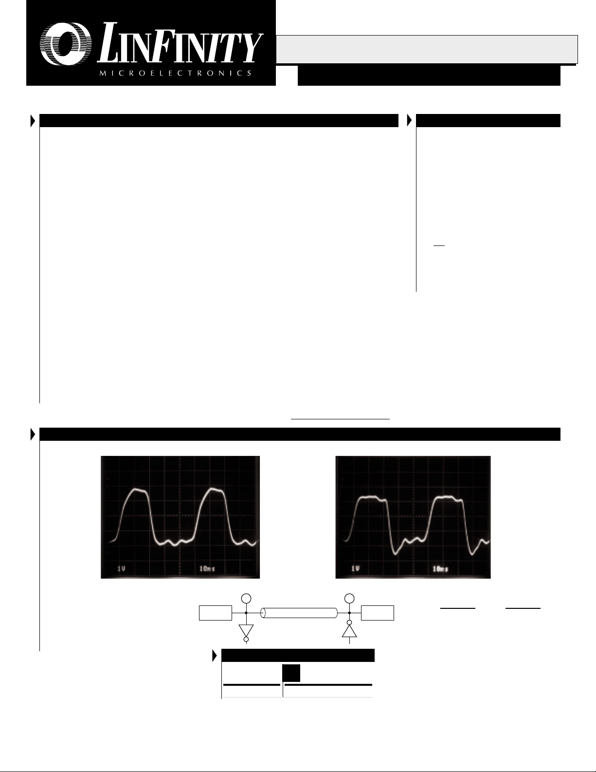
DRIVING WAVEFORM - 20MHZRECEIVING WAVEFORM - 20MHZ
Receiver
1 Meter, AWG 28
LX5122 LX5122
LX5268 LX5268
PACKAGE ORDER INFO
T
(°C)
J
0 to 125 LX5122CDB
Append the letter "T" to part number. (i.e. LX5122CDBT)
Note: Available in Tape & Reel.
Plastic SSOP
DB
44-pin
Driver
NOTE:
For An In-Depth
Discussion On Applying
SCSI, Request Linfinity
Application Note:
"Understanding The
Single-Ended SCSI Bus"
Copyright © 1999
Rev. 1.0 6/99
L INF INITY MICROELECTRONICS INC.
11861 WESTERN AVENUE, GARDEN GROVE, CA. 92841, 714-898-8121, FAX: 714-893-2570
1
Page 2
PRODUCT DATABOOK 1996/1997
LX5122
ULTRA 27-LINE, PLUG AND PLAY SCSI TERMINATOR
P RODUCTION DATA SHEET
ABSOLUTE MAXIMUM RATINGS (Note 1)
TermPwr Voltage ..................................................................................................... 7V
Continuous Output Voltage Range .............................................................. 0 to 5.5V
Continuous Disable Voltage Range.............................................................. 0 to 5.5V
Operating Junction Temperature
Plastic (PW & DB Packages)......................................................................... 150ºC
Storage Temperature Range ............................................................. -65°C to +150°C
Solder Temperature (Soldering, 10 seconds) ................................................... 300°C
Note 1. Exceeding these ratings could cause damage to the device.
THERMAL DATA
PW PACKAGE:
THERMAL RESISTANCE-JUNCTION TO AMBIENT,
DB PACKAGE:
THERMAL RESISTANCE-JUNCTION TO AMBIENT,
Junction Temperature Calculation: TJ = TA + (PD x θJA).
The θJA numbers are guidelines for the thermal performance of the device/pc-board
system. All of the above assume no ambient airflow.
θθ
θ
θθ
JA
θθ
θ
θθ
JA
50°C/W
50°C/W
UltraMAX
PACKAGE PIN OUTS
T19
T20
W1
W2
GND
GND
GND
GND
DISC1
DISC2
T10
T21
T22
144
243
342
T1
441
T2
540
639
738
T3
837
T4
936
T5
10 35
11 34
12 33
13 32
14 31
15 30
16 29
T6
17 28
T7
18 27
T8
19 26
T9
20 25
21 24
22 23
DB PACKAGE
(Top View)
T27
T26
T25
T18
N1
T17
T16
T15
N.C.
GND
GND
GND
GND
V
T
T14
T13
T12
N.C.
N.C.
T11
T24
T23
RECOMMENDED OPERATING CONDITIONS (Note 2)
Parameter
Termination Voltage V
High Level Disable Input Voltage V
Low Level Disable Input Voltage V
Operating Virtual Junction Temperature Range
LX5122C
Note 2. Range over which the device is functional.
Symbol
TERM
IH
IL
Recommended Operating Conditions
Min. Typ. Max.
Units
4.0 5.5 V
2V
TERM
V
0 0.8 V
0 125 °C
ELECTRICAL CHARACTERISTICS
Term Power = 4.75V unless otherwise specified. Unless otherwise specified, these specifications apply at the recommended operating ambient temperature of TA = 25°C. Low duty cycle pulse testing techniques are used which maintains junction and case temperatures equal to the ambient temperature.
Parameter
Output High Voltage V
TermPwr Supply Current I
Symbol
OUT
CC
Test Conditions Units
All data lines = open
All data lines = 0.5V
DISC1 and DISC2 < 0.8V
Output Current I
Disable Input Current DISC1 I
OUTVOUT
IN
= 0.2V
DISC1 = 0V
DISC2 DISC2 = 0V
Output Leakage Current DISC1 and DISC2 < 0.8V, VO = 0.2V
Channel Bandwidth BW
Termination Sink Current, per Channel I
SINKVOUT
= 4V
LX5122
Min. Typ. Max.
2.65 2.85 V
12 20 mA
635 670 mA
50 150 µA
-20 -23 -24 mA
-10 µA
-10 µA
1µA
35 MHz
7mA
2
Copyright © 1999
Rev. 1.0 6/99
Page 3

PRODUCT DATABOOK 1996/1997
UltraMAX
V
V
CC
DISC1
CC
DISC2
1.4V
ULTRA 27-LINE, PLUG AND PLAY SCSI TERMINATOR
P RODUCTION DATA SHEET
BLOCK DIAGRAM
TERM POWER
CURRENT
BIASING
CIRCUIT
24mA CURRENT
LIMITING CIRCUIT
2.85V
LX5122
DATA OUTPUT
PIN DB(0)
1 OF 27 CHANNELS
FUNCTIONAL DESCRIPTION
Cable transmission theory suggests that in order to optimize
signal speed and quality, the termination should act both as
an ideal voltage reference when the line is released (de-asserted)
and as an ideal current source when the line is active (asserted).
Common active terminators, which consist of Linear Regulators
in series with resistors (typically 110Ω), are a compromise. As
the line voltage increases, the amount of current decreases
linearly by the equation V = I * R. The UltraMAX LX5122, with
its unique new architecture, applies the maximum amount of
current regardless of line voltage until the termination high
threshold (2.85V) is reached.
Acting as a near ideal line terminator, the LX5122 closely
reproduces the optimum case when the device is enabled. To
enable the device the DISC1 and DISC2 pins must be driven
POWER UP / POWER DOWN FUNCTION TABLE
DISC1 DISC2 W1 W2 N1 T1-T18 T19-T27
L H DC DC DC Enabled
H L DC DC DC
H H DC DC DC
Disabled
Disabled Disabled
L L H H H Enabled Enabled
L L H H L Enabled Enabled
L L H L H Enabled Enabled
LLHLL
Disabled
L L L H H Enabled Enabled
LLLHL
LLLLH
L L LLL
Disabled
Disabled Disabled
Disabled Disabled
Disabled
Enabled
Enabled
Enabled
per the above table. During this mode of operation,
quiescent current is 12mA and the device will
respond to line demands by delivering 24mA on
assertion and by imposing 2.85V on de-assertion.
Disable mode places the device in a sleep state,
where a meager 150µA of quiescent current is
consumed. Additionally, all outputs are in a HiZ (impedance) state. Sleep mode can be used
for power conservation or to completely eliminate
the terminator from the SCSI chain.
An additional feature of the LX5122 is its compatibility with active negation drivers.
Copyright © 1999
Rev. 1.0 6/99
3
Page 4

PRODUCT DATABOOK 1996/1997
LX5122
ULTRA 27-LINE, PLUG AND PLAY SCSI TERMINATOR
P RODUCTION DATA SHEET
PLUG AND PLAY SCSI DIAGRAM
Internal Narrow
Internal Wide
LX5122
UltraMAX
External
Wide
For Plug and Play SCSI auto-termination diabling, connect pin 50 of the External Wide SCSI connector to W1 of the LX5122,
connect pin 50 of the Internal Wide SCSI connector to W2 of the LX5122, and connect pin 22 of the Internal Narrow connector
to N1 of the LX5122.
PRODUCTION DATA - Information contained in this document is proprietary to LinFinity, and is current as of publication date. This document
may not be modified in any way without the express written consent of LinFinity. Product processing does not necessarily include testing of
all parameters. Linfinity reserves the right to change the configuration and performance of the product and to discontinue product at any time.
4
UltraMAX is a trademark of Linfinity Microelectronics Inc.
Copyright © 1999
Rev. 1.0 6/99
 Loading...