

Page 1
Low Current Quad
Inverting Amplifiers
LX509 - DATA SHEET
FEATURES
µA typical current drain
• 210
• 4 inverting opamps; B with 6 dB greater drive current
• minimum 46 dB open loop gain
• ideal for - active filtering
- dual channel hearing aids
- mixers
- microphone / telecoil preamps
STANDARD PACKAGING
• 10 pin PLID
• 10 pin SLT
• Chip (61 x 55 mils)
®
Au Bump
DESCRIPTION
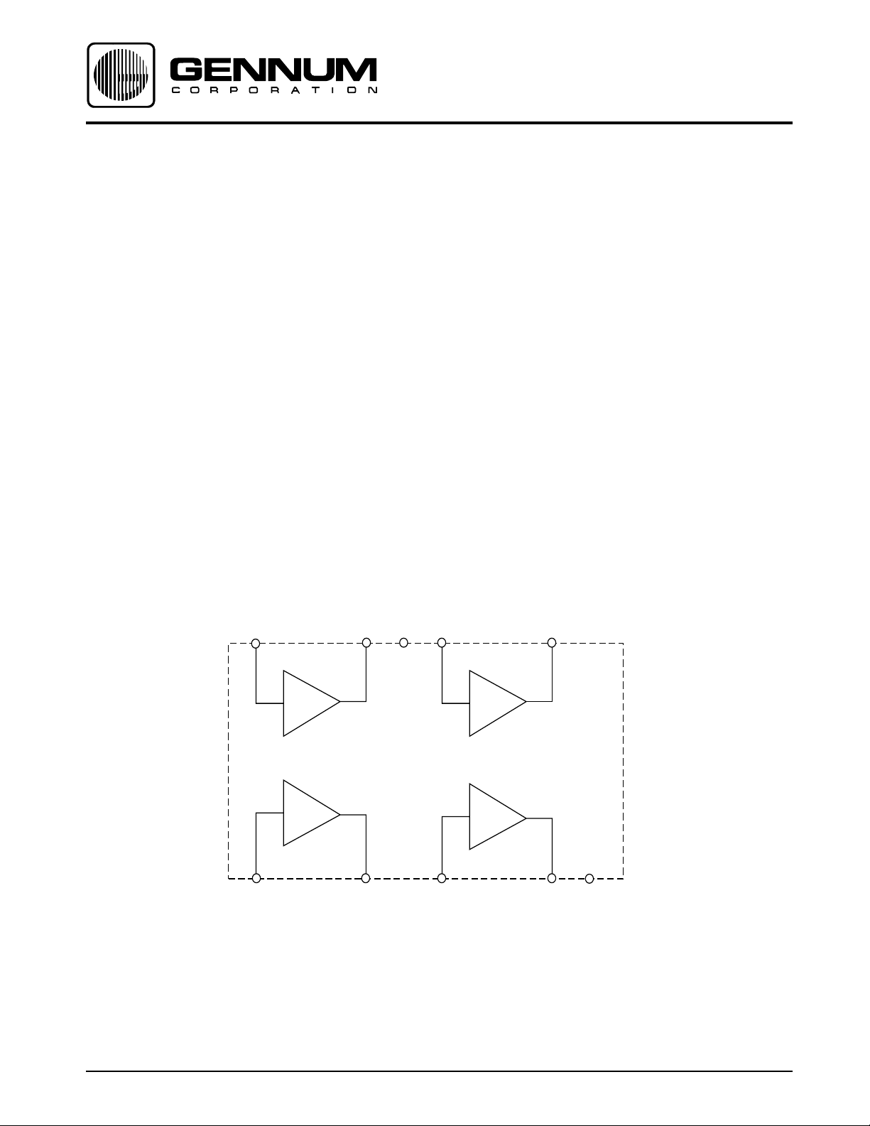
The LX509 consists of 4 independent low noise, low current
inverting operational amplifiers utilizing Gennum's low voltage
bipolar JFET technology. Each amplifier has a minimum open
loop gain of 46 dB with the closed loop gain set by the ratio of
a feedback (R
a well controlled gain tolerance from amplifier to amplifier, it is
recommended that the closed loop gain is at least 20 dB below
the open loop gain.
Three of the preamplifiers, A, C and D are capable of delivering
typically 30 µA of peak current drive while the fourth preamplifier B has 6 dB more current drive capability, allowing a
6 dB greater output into the same load impedance, or the same
output level into one half the load impedance.
) resistor to the source impedance (RS) . For
F
C
IN
C
OUT
V
D
B
IN
D
OUT
6 7 8 9 10
- C
- B
- D
- A
5 4 3 2 1
B
IN
B
OUT
BLOCK DIAGRAM
A
IN
A
OUT
GND
Revision Date: January 2001
GENNUM CORPORATION P.O. Box 489, Stn. A, Burlington, Ontario, Canada L7R 3Y3 tel. +1 (905) 632-2996
Document No. 510 - 30 - 06
Web Site: www.gennum.com E-mail: hipinfo@gennum.com
Page 2
ABSOLUTE MAXIMUM RATINGS
PIN CONNECTION
PARAMETER VALUE / UNITS
Supply Voltage 5V DC
Operating Temperature -10o to +40oC
Storage Temperature -20o to +70oC
CAUTION
CLASS 1 ESD SENSITIVITY
B IN
B OUT
A IN
A OUT
GND
5
1
6
10
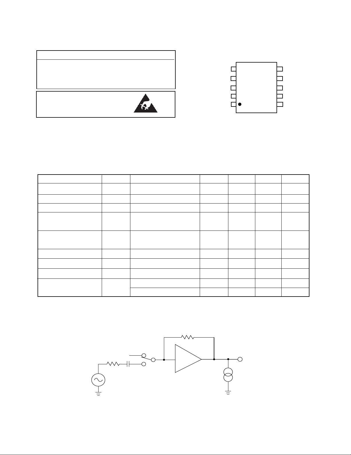
ELECTRICAL CHARACTERISTICS
V
Pin voltage measured with conditions as shown in Test Circuit
OUT
Positive Current corresponds to current INTO the pin
Negative Current corresponds to current OUT of the pin
Conditions: Frequency = 1 kHz, Temperature = 25
PARAMETER SYMBOL CONDITIONS MIN TYP MAX UNITS
o
C, Supply Voltage VB = 1.3 VDC
C IN
C OUT
V
B
D IN
D OUT
Total Current I
Input Bias Voltage V
Input Bias Current I
Output Voltage Swing - Hi V
Output Voltage Swing - Lo V
Open Loop Voltage Gain A
TOT
BIAS
BIAS
VOL
OH
OL
RF = 1 MΩ -50 0 50 nA
V
= 0.4 VDC
IN
I
= -10 µA, (Note 1)
L
I
= +1 µA
IN
I
= +10 µA, (Note 2)
L
= ∞ 200 580 - mVDC
' RF
= ∞ 200 280 - mVDC
' RF
115 210 305 µA
500 570 620 mVDC
46 56 - dB
Input Referred Noise IRN NFB 0.2 to 10kHz at 12dB/Oct - 1 - µVRMS
Harmonic Distortion THD - 1 - %
Current Drive A, C, D, - 30 - µA
Capability B - 60 - µA
All Parameters and Switches remain as shown in Test Circuit unless otherwise stated in "Conditions" Column
Notes: 1 V
2 V
OH
OL
= V
= V
180 µV
at 1kHz
OUT
OUT
- V
(IL = -10 µA for Blocks A, C, D, I
OUT
- V
(I
= +10 µA for Blocks A, C, D, I
OUT
L
V
C
RMS
R
3.92k
S
S
1.0
= -20 µA for Block B)
L
= +20 µA for Block B)
L
= 0
R
F
a
IN
S1
-A to -D
b
V
OUT
= 0
I
L
510 - 30 - 06
All resistors in ohms, all capacitors in µF unless otherwise stated
Fig. 1 LX509 Test Circuit
2
Page 3

10
9
2
8
4
7
1
6
5
BASE
CURRENT
COMPENSATION
3
Fig. 2 Functional Schematic
R
F
C11
V1
MIC
V1
V2
V3
V2
TELE
COIL
R2
R3
R
1
IN
2
R
IN
Fig. 3b Mixing Circuit
C4
C1
C2
R1
- A
Fig. 3a Summing Amplifier
R
1
F
- A
- C
R
2
F
C1
4.7k
T
4.7k
C2
R1
- A
R2
M
T
- C
R2
C3
- A
- C
R1
- D
C2
R12
R5
C5
High Pass
Band Pass
Low Pass
C10
C9
C8
R10
R9
R8
R11
- B
V
O
V
O
V1
- B
R3
C1
C4
V3
C7
R3
R6
V2
V
O
C1
R2
C3
R4
R7
C6
Fig. 3d Multi-Band Filtering
R3
- B
(for Filter Design refer to Note 600-9, Active Filtering for Hearing Aids)
R
F
V
O
All resistors in ohms, all capacitors in µF unless otherwise stated
Fig. 3c Mic / Telecoil Preamplifier
Fig. 3 LX509 Application Circuits
3
510 - 30 - 06
Page 4

0
-20
-40
= 47k
R
-60
-80
OUTPUT (dBV)
-100
-120
F
-130 -110 -90 -70 -50 -30 -10
R
= 100k
F
R
F
R
= 22k
F
INPUT (dBV)
= 10k
Fig. 4 I/O Characteristics for
Various RF Values
4
C
= 0.22µ
0
-4
R
= 3.3k
F
-8
-12
RELATIVE OUTPUT (dB)
-16
-20
20 200 2k 20k
S
C
= 0.1µ
S
C
= 0.033µ
S
C
= 0.047µ
S
FREQUENCY (Hz)
Fig. 5 Closed Loop Frequency Response
for Various CS Values
4
0
-4
-8
-12
RELATIVE GAIN (dB)
-16
0.6 0.7 0.8 0.9 1.0 1.1 1.2 1.3 1.4
-20
SUPPLY VOLTAGE (V)
Fig. 6 Gain vs Supply Voltage
40
20
0
-20
60
55
50
45
40
GAIN (dB)
35
30
25
10 100 1k 10k 100k
20
FREQUENCY (Hz)
Fig. 7 Preamplifier Open Loop Frequency
Response
-40
RELATIVE TOTAL CURRENT (µA)
-60
-20 -10 0 10 20 30 40 50
TEMPERATURE (oC)
Fig.8 Total Current vs Temperature
GENNUM CORPORATION
MAILING ADDRESS:
P.O. Box 489, Stn. A, Burlington, Ontario, Canada L7R 3Y3
Tel. +1 (905) 632-2996 Fax +1 (905) 632-2814
SHIPPING ADDRESS:
970 Fraser Drive, Burlington, Ontario, Canada L7L 5P5
GENNUM JAPAN CORPORATION
C-101, Miyamae Village, 2-10-42 Miyamae, Suginami-ku, Tokyo 168-0081,
Japan Tel. +81 (3) 3334-7700 Fax: +81 (3) 3247-8839
Gennum Corporation assumes no responsibility for the use of any circuits described herein and makes no representations that they are free from patent infringement.
510 - 30 - 06
DOCUMENT IDENTIFICATION: DATA SHEET
The product is in production. Gennum reserves the right to make
changes at any time to improve reliability, function or design, in
order to provide the best product possible.
REVISION NOTES:
Changes to standard packaging information.
© Copyright July 1988 Gennum Corporation. All rights reserved. Printed in Canada.
4
 Loading...