

Datasheet LX432ISE, LX432ISC, LX432CSC, LX432CLP, LX432ILP Datasheet (Microsemi Corporation)
...Page 1
LX432
A
LOW VOLTAGE ADJUSTABLE PRECISION SHUNT REGULATORS
T HE I NFINITE P OWER OF I NNOVATION
DESCRIPTION KEY FEATURES
The LX432 series are low-voltage precision adjustable shunt regulators
with a reference voltage of 1.24V. The
output voltage may be set to any value
between 1.24V and 20V by two external
resistors.
These devices offer low output im-
pedance for improved load regulation — typical output impedance is
250mΩ. The LX432 series operates with
an operating current as low as 80µA,
making these devices suitable for portable and micropower applications.
IMPORTANT: For the most current data, consult LinFinity's web site: http://www.linfinity.com.
Low voltage operation enables the
LX432 to be used in the feedback loop
of isolated low voltage power supplies. The minimum output voltage is
determined by the LX432 output voltage
plus the forward voltage drop of the
opto-coupler LED (typically 1.24 + 1.4 =
2.64V minimum). See Figure 10.
The LX432 is offered in 3 and 5-pin
SOT-23 or TO-92 packages, and is a dropin replacement for the TLV431 and
SC431L devices.
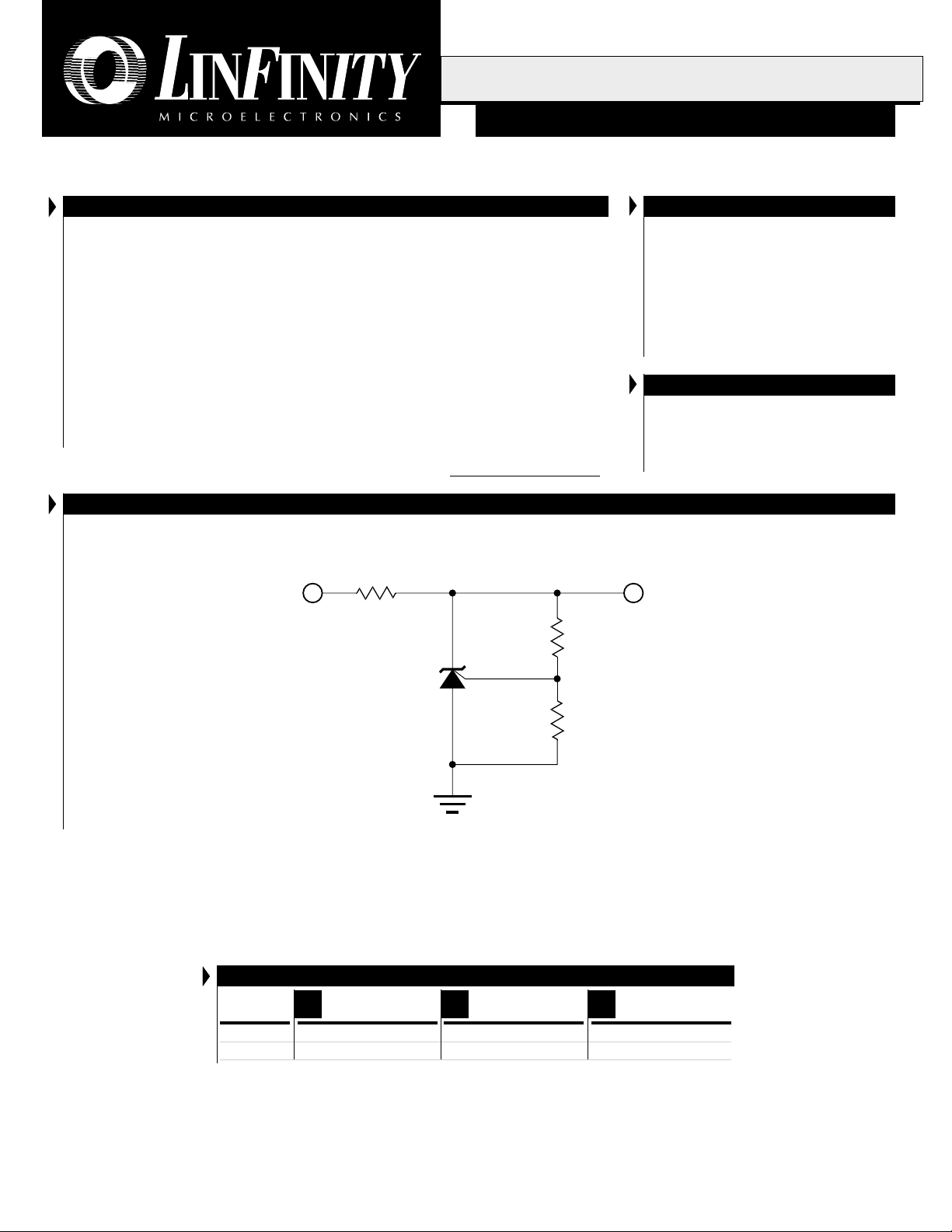
PRODUCT HIGHLIGHT
T YPICAL PROGRAMMABLE VOLTAGE
REFERENCE CIRCUIT
V
IN
P RODUCTION DATA SHEET
■ Low Voltage Operation: 1.24V Reference
■ Initial Voltage Reference Accuracy 1%
■ Adjustable Output Voltage From V
■ Typical Output Dynamic Impedance Less
Than 250mΩ
■ Sink Current Capability 80µA To 20mA
■ Direct Alternative To TLV431
APPLICATIONS
■ Low Voltage Adjustable Power Supplies
■ Instrumentation
■ Computers
■ Portable Equipment
V
K
To 20V
REF
Cathode
LX432
Anode
Reference
R2
GND
PACKAGE ORDER INFORMATION
R1
T
(°C)
A
0 to 70 LX432CSC LX432CSE LX432CLP
-40 to 85 LX432ISC LX432ISE LX432ILP
Plastic SOT-23
SC
3-pin
Note: All surface-mount packages are available in Tape & Reel.
Append the letter "T" to part number. (i.e. LX432CSET)
TO-92 (LP) package also available in ammo-pack.
Plastic SOT-23
SE
5-pin
Plastic TO-92
LP
3-pin
Copyright © 1999
Rev. 1.0 9/99
L INF INITY MICROELECTRONICS INC.
11861 WESTERN AVENUE, GARDEN GROVE, CA. 92841, 714-898-8121, FAX: 714-893-2570
1
Page 2
LX432
PRODUCT DATABOOK 1996/1997
LOW VOLTAGE ADJUSTABLE PRECISION SHUNT REGULATORS
P RODUCTION DATA SHEET
ABSOLUTE MAXIMUM RATINGS (Note 1)
Cathode to Anode Voltage (VKA) ................................................................. -0.3V to +20V
Reference Input Current (I
Continuous Cathode Current (I
Operating Junction Temperature
) .................................................................... -50µA to 10µA
REF
) ............................................................. -25mA to 25mA
K
Plastic (SC, SE & LP Packages) ............................................................................. 150°C
Storage Temperature Range ...................................................................... -65°C to 150°C
Lead Temperature ..................................................................................................... 300°C
Note 1. Exceeding these ratings could cause damage to the device. All voltages are with respect
to Ground. Currents are positive into, negative out of the specified terminal. Pin
numbers refer to DIL packages only.
THERMAL DATA
SC PACKAGE:
Thermal Resistance - Junction to Ambient,
SE PACKAGE:
Thermal Resistance - Junction to Ambient,
LP PACKAGE:
Thermal Resistance-Junction to Ambient,
Junction Temperature Calculation: TJ = TA + (P
The θ
numbers are guidelines for the thermal performance of the device/pc-board system.
JA
All of the above assume no ambient airflow
θθ
θ
(PC-Mounted) 220°C/W
θθ
JA
(Non-PC Mounted) 410°C/W
θθ
θ
(PC-Mounted) 220°C/W
θθ
JA
(Non-PC Mounted) 410°C/W
θθ
θ
θθ
JA
x θ
).
D
JA
156°C/W
PACKAGE PIN OUTS
2
CATHODE
ANODE
SC PACKAGE — 3-Pin
N.C.
N.C.
CATHODE
SE PACKAGE — 5-Pin
3
1
(Top View)
15
2
34
(Top View)
REF
ANODE
REF
3. CATHODE
2. ANODE
1. REF
Ref (R)
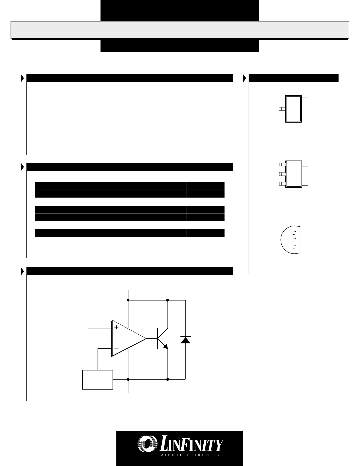
BLOCK DIAGRAM
Cathode (K)
V
REF
Anode (A)
LP PACKAGE
(Top View)
2
Copyright © 1999
Rev. 1.0 9/99
Page 3
PRODUCT DATABOOK 1996/1997
LX432
LOW VOLTAGE ADJUSTABLE PRECISION SHUNT REGULATORS
P RODUCTION DATA SHEET
ELECTRICAL CHARACTERISTICS
(Unless otherwise specified, these specifications apply over the operating ambient temperatures for LX432C with 0°C ≤ TA ≤ 70°C, and the LX432I
with -40°C ≤ TA ≤ 85°C.)
Parameter
Reference Voltage V
Reference Voltage Drift
Ratio Of V
Change In Cathode ∆V
REF
Voltage Change
Reference Terminal Current I
Reference Current Drift (Note 2) ∆I
Minimum Cathode Current For Regulation I
Dynamic Impedance Z
Off-state Cathode Current I
(Note 2) ∆V
(Note 3) ∆V
Symbol
REFIK
REFIK
REFIK
KA
REFIK
REFIK
K (MIN)VKA
KAIK
OFFVKA
Note 2. These parameters are guaranteed by design.
∆V
Note 3. Ratio of change in reference input voltage
REF
∆V
KA
to the change in cathode voltage.
Test Conditions
= 10mA, VKA = V
= 10mA, VKA = V
IK = 10mA, VKA = V
= 10mA, VKA = V
= 10mA, VKA = V
= 10mA, VKA = V
IK = 10mA, VKA = V
= V
, TA = 25°C
REF
= 0.1mA to 15mA, VKA = V
= 16V, TA = 25°C
, TA = 25°C
REF
, 0°C ≤ TA ≤ 70°C
REF
, -40°C ≤ TA ≤ 85°C
REF
to 16V, TA = 25°C
REF
, T
= 25°C, R1=10kΩ, R2 = Open
REF
A
, 0°C ≤ TA ≤ 70°C
REF
, -40°C ≤ TA ≤ 85°C
REF
, TA = 25°C
REF
LX432
Min. Typ. Max.
Units
1.228 1.24 1.252 V
312 mV
420 mV
-1 -2.7 mV/V
0.1 0.5 µA
0.05 0.3 µA
0.1 0.4 µA
55 80 µA
0.2 0.4 Ω
0.004 µA
Copyright © 1999
Rev. 1.0 9/99
3
Page 4

LX432
PRODUCT DATABOOK 1996/1997
LOW VOLTAGE ADJUSTABLE PRECISION SHUNT REGULATORS
P RODUCTION DATA SHEET
GRAPH / CURVE INDEX
Characteristic Curves
FIGURE #
1. Reference Voltage vs. Junction Temperature
2. Reference Current vs. Junction Temperature
3. Cathode Current vs. Cathode Voltage
4. ∆V
5. Dynamic Impedance vs. Junction Temperature
6. Minimum Cathode Current For Regulation vs. Junction
7. Off-State Current vs. Junction Temperature
8. Equivalent Input Noise Voltage vs. Frequency
/ ∆V
REF
KA
Temperature
vs. Junction Temperature
FIGURE INDEX
Parameter Measurement Information
FIGURE #
9. Test Circuit For V
10. Test Circuit For VKA > V
11. Test Circuit For I
= V
KA
REF
REF
OFF
Typical Applications
FIGURE #
12. Flyback With Isolation Using LX431 Or LX431A As Voltage
Reference And Error Amplifier
13. LX432 In 3.3V To 2.7V Low Dropout Regulator Application
4
Copyright © 1999
Rev. 1.0 9/99
Page 5

PRODUCT DATABOOK 1996/1997
LOW VOLTAGE ADJUSTABLE PRECISION SHUNT REGULATORS
P RODUCTION DATA SHEET
CHARACTERISTIC CURVES
LX432
: Reference Voltage (V)
REF
V
1.25
1.245
1.24
1.235
1.23
-40-30-20-100 102030405060708090
TJ : Junction Temperature ( C)
: Reference Current ( A)
REF
I
0.2
0.16
0.12
0.08
0.04
0
-40-30-20-100 102030405060708090
TJ : Junction Temperature ( C)
FIGURE 1 — Reference Voltage vs. Junction Temperature FIGURE 2 — Reference Current vs. Junction Temperature
800
700
600
500
400
300
200
100
: Cathode Current ( A)
K
I
0
-100
-200
-1 -0.5 0 0.5 1 1.5
-1.200
-1.000
-0.800
(mV/V)
KA
V
∆
∆∆
∆
/
-0.600
REF
V
∆
∆∆
∆
-0.400
-0.200
-40-30-20-100 102030405060708090
Copyright © 1999
Rev. 1.0 9/99
TJ : Junction Temperature (V)
TJ : Junction Temperature ( C)
FIGURE 3 — Cathode Current vs. Cathode Voltage FIGURE 4 — ∆V
REF
/ ∆V
vs. Junction Temperature
KA
5
Page 6

LX432
PRODUCT DATABOOK 1996/1997
LOW VOLTAGE ADJUSTABLE PRECISION SHUNT REGULATORS
P RODUCTION DATA SHEET
CHARACTERISTIC CURVES
1.000
0.800
0.600
0.400
0.200
Dynamic Impedance (Ohm)
0.000
-40-30-20-100 102030405060708090
TJ : Junction Temperature ( C)
120
100
80
60
40
20
Minimum Cathode Current ( A)
0
-40-30-20-100 102030405060708090
TJ : Junction Temperature ( C)
FIGURE 5 — Dynamic Impedance vs. Junction Temperature FIGURE 6 — Minimum Cathode Current for Regulation
vs. Junction Temperature
0.012
350
0.010
300
0.008
0.006
0.004
Off-State Current ( A)
0.002
0.000
-40-30-20-100 102030405060708090
TJ : Junction Temperature ( C)
250
200
Noise Voltage (nV/sqrt(Hz))
150
10 100 1K 10K 100K
Frequency (Hz)
FIGURE 7 — Off-State Current vs. Junction Temperature FIGURE 8 — Equivalent Input Noise Voltage vs. Frequency
6
Copyright © 1999
Rev. 1.0 9/99
Page 7

PRODUCT DATABOOK 1996/1997
A
A
A
LOW VOLTAGE ADJUSTABLE PRECISION SHUNT REGULATORS
P RODUCTION DATA SHEET
PARAMETER MEASUREMENT INFORMATION
LX432
Input
V
REF
FIGURE 9 — Test Circuit For VKA = V
I
K
Input
V
K
REF
Input
R
1
I
REF
R
FIGURE 10 — Test Circuit For VKA > V
V
I
OFF
V
2
K
REF
I
K
V
K
REF
Copyright © 1999
Rev. 1.0 9/99
FIGURE 11 — Test Circuit For I
OFF
7
Page 8

LX432
110/220V AC
PRODUCT DATABOOK 1996/1997
LOW VOLTAGE ADJUSTABLE PRECISION SHUNT REGULATORS
P RODUCTION DATA SHEET
TYPICAL APPLICATION
V
IN
V
OUT
3.3V
Controller
UC384x/LX155x
FIGURE 12 — LX432 In A Power Supply Isolated Feedback Application
0.1µF
500
DRV
V
CC
I
SENSE
V
GND
FB
12V 3.3V
9
9
140
470µF
LX432
0.1µF
2.7V
(e .g . In te l i7 4 0® chipset)
LX 432
1000µF
9
120
FIGURE 13 — LX432 In 3.3V To 2.7V Low Dropout Regulator Application
PRODUCTION DATA - Information contained in this document is proprietary to LinFinity, and is current as of publication date. This document
may not be modified in any way without the express written consent of LinFinity. Product processing does not necessarily include testing of
all parameters. Linfinity reserves the right to change the configuration and performance of the product and to discontinue product at any time.
8
0.1µF
Copyright © 1999
Rev. 1.0 9/99
 Loading...