

Page 1
RangeMAX
)
D IGITAL DIMMING CCFL CONTROLLER IC
TM
LX1686
T HE I NFINITE P OWER OF I NNOVATION
DESCRIPTION KEY FEATURES
The LX1686 Backlight Controller IC
provides all the control functions needed
to implement Linfinity’s direct drive inverters used to operate cold cathode fluorescent lamps (CCFL’s). This IC can be
used to control single or multiple-lamp
configurations. CCFL’s are used for back
or edge lighting of liquid crystal flat panel
displays (LCD’s) and typically find application in notebook computers, web
browsers, automotive and industrial instrumentation, and entertainment systems.
The LX1686 includes a PWM con-
trolled lamp current burst circuit that
can provide a >100:1 dimming range from
a simple zero to 2.5V potentiometer input. The PWM dimming burst rate is
easily synchronized to the LCD panel’s
frame rate to prevent interference from
optical beat frequencies.
NOTE: For current data & package dimensions, visit our web site: http://www.linfinity.com.
Safety and reliability features in-
clude a new dual feedback contol loop
that permits regulation of maximum lamp
strike voltage as well as lamp current.
Regulating maximum lamp voltage permits the designer to provide for ample
worst case lamp strike voltage while at
the same time conservatively limit maximum open circuit voltage.
An innovative new strike voltage
generation technique enables the mod-
ule designer to optimize high voltage
transformer design for maximum operating efficiency with no power dissipating overhead to guarantee strike capability.
Direct drive topology is a non-resonant, oscillator-controlled PWM regulation method. The LX1686 allows a
wide choice of fixed operating frequencies to match lamp current frequency to
the lamp’s most efficient operating point,
and to minimize high frequency interference.
P RELIMINARY DATA SHEET
■ RangeMAX
■ Synchronizable To Display Video Frequency
■ High Voltage Feedback Loop Directly
Controls Maximum Open Lamp And
Minimum Strike Voltages
■ Transformer Protected From Over-Heating
During Lamp Striking
■ Micro-Amp Sleep Mode
■ User-Programmable Fixed Frequency
Operation
■ Under-Voltage Lockout Feature With Power-
Up Reset
■ Built-In Soft-Start Feature
■ Operates With 3.3V or 5V Power Supplies
■ 100mA Output Drive Capability
■ Notebooks
■ Instrumentation Displays
■ Desktop Computer Monitors
■ Low Ambient Light Displays (used in
Aircraft, Automobiles, and Hand-held
Equipment)
■ Extemely High Efficiency From 3.3V or 5V
Power Supplies
■ Lower Cost Than Conventional Buck / Royer
Inverter Topologies
■ Improved Lamp Strike Capability
■ Improved Over-Voltage Control
TM
Wide Range Dimming (>100:1)
APPLICATIONS
BENEFITS
Power Used (Watts)
Copyright © 2000
Rev. 0.4 1/00
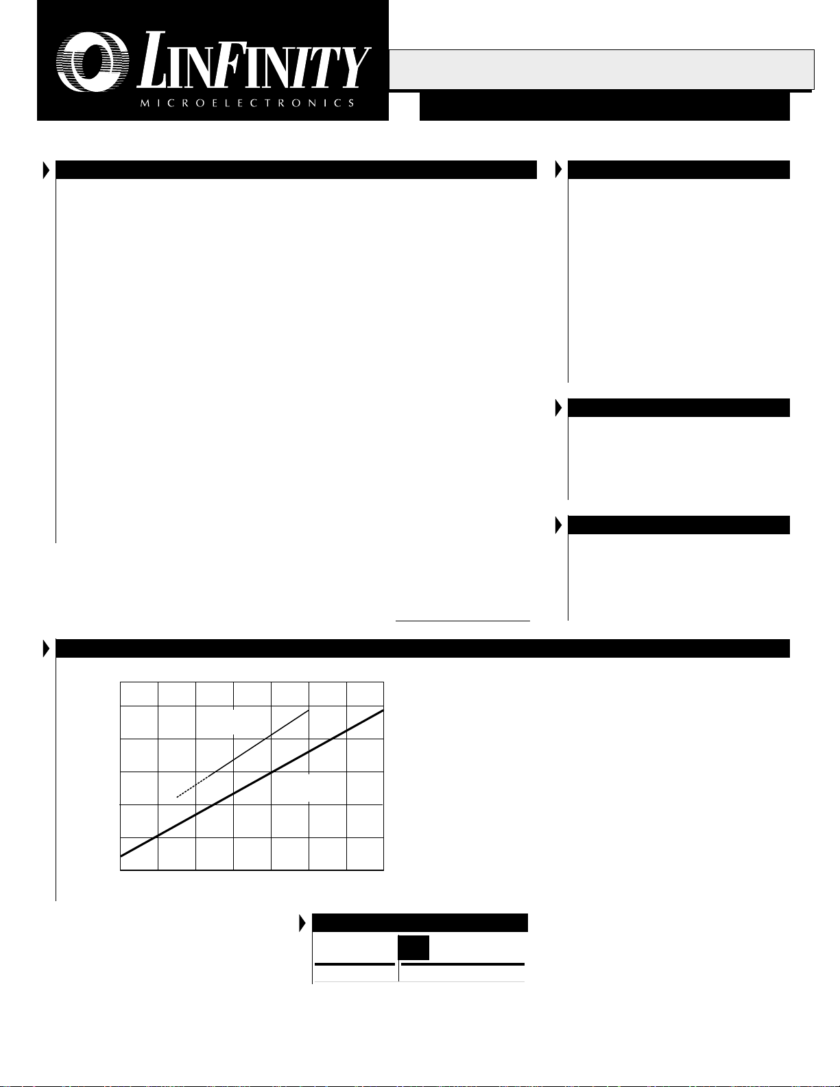
RANGEMAX VS. ANALOG DIMMING
5
4
3
2
1
0
30 45
Standard Analog
Dimming Inverter
60
75 90 105
Light Output (Nits
Note: All surface-mount packages are available in Tape & Reel.
LinFinity's
RangeMAX
Append the letter "T" to part number. (i.e. LX1686CPWT)
L INF INITY MICROELECTRONICS INC.
11861 WESTERN AVENUE, GARDEN GROVE, CA. 92841, 714-898-8121, FAX: 714-893-2570
PRODUCT HIGHLIGHT
Light emitted by a CCFL is proportional to the current
flowing through it. There are two ways to control the
current: by adjusting the amplitude of a continuous AC
current; or, as with RangeMAX technology, by varying
the amount of time a burst of full current is present.
RangeMAX technology frees the backlight inverter
module designer to operate in a lower brightness and
lower power consumption mode than is possible with
conventional amplitude control methods.
PACKAGE ORDER INFO
T
(°C)
A
0 to 85 LX1686CPW
Plastic TSSOP
PW
24-pin
1
Page 2
PRODUCT DATABOOK 1996/1997
LX1686
D IGITAL DIMMING CCFL CONTROLLER IC
P RELIMINARY DATA SHEET
ABSOLUTE MAXIMUM RATINGS (Note 1)
Supply Voltage (VDD, VDD_P) ......................................................................... 6.5V
Digital Inputs .................................................................................. -0.3 to VDD+0.5V
Analog Inputs .................................................................................. -0.3 to VDD+0.5V
Digital Outputs ................................................................................ -0.3 to VDD+0.5V
Analog Outputs ............................................................................... -0.3 to VDD+0.5V
Operating Junction Temperature
Plastic (DB, PW Packages) .......................................................................... 150°C
Storage Temperature Range .............................................................. -65°C to 150°C
Lead Temperature (Soldering, 10 seconds) .................................................... 300°C
Note 1. Exceeding these ratings could cause damage to the device. All voltages are with
PW PACKAGE:
Junction Temperature Calculation: TJ = TA + (P
The θ
system. All of the above assume no ambient airflow.
respect to Ground. Currents are positive into, negative out of the specified
terminal.
THERMAL DATA
D
x θ
θθ
θ
θθ
JA
).
JA
THERMAL RESISTANCE-JUNCTION TO AMBIENT,
numbers are guidelines for the thermal performance of the device/pc-board
JA
100°C/W
RangeMAX
PACKAGE PIN OUTS
AOUT
VSS_P
VSS
AFD_C
RAMP_C
RAMP_R
FVERT
PD_CR
VCO_C
BRT_POS
BRITE
DIG_DIM
1 24
223
322
421
520
619
718
817
916
10 15
11 14
12 13
PW PACKAGE
(Top View)
TM
BOUT
VDD_P
VDD
TRI_C
OLSNS
ISNS
ICOMP
VSNS
VCOMP
BRT
I_R
ENABLE
ELECTRICAL CHARACTERISTICS
(Unless otherwise specified, these specifications apply over the recommended operating conditions of TA = 0 to 85°C, VDD=VDD_P= 3.0 to 5.5V)
(Ri = 40kΩ, C
Power Supply Voltage VDD VDD = VDD_P
Operating Current I
Power Supply Voltage VDD_P VDD = VDD_P
Output Buffer Operating Current I
UVLO Threshold V
UVLO Hysteresis V
= 0.01µF, C
VCO
= 0.22µF, C
AFD
Parameter
= 0.83µF, C
TRI
= 208pF, R
RAMP
Symbol
DD
DD_P
TH_UVLO
H_UVLO
= 15kΩ, C
RAMP
= 0.22µF, C
PD
= 0.047µF, R
PDC
Test Conditions Units
VDD = VDD_P = 5V
Volsns = VDD = VDD_P = 5V, CA = CB = 1000pF
= 110kΩ.)
PD
LX1686
Min. Typ. Max.
35.5V
57mA
35.5V
210mA
2.7 2.9 V
160 mV
Direct Drive Ramp Block
Triangular Wave Generator Analog Output Peak Voltage V
Triangular Wave Generator Analog Output Valley Voltage
Triangular Wave Generator Oscillation Frequency F
Triangular Wave Generator Oscillation Charge Current I
Triangular Wave Generator Oscillation Discharge Current
I
DISCHG_TRI
Ramp Generator Analog Output Peak Voltage V
Ramp Generator Analog Output Valley Voltage V
Ramp Frequency Change Threshold V
Ramp Generator Oscillation Frequency - Nominal F
Ramp Generator Oscillation Frequency - Maximum F
OLSNS Threshold Voltage V
OLSNS Hysteresis V
OLSNS-to-ICOMP Propagation Delay T
P_TRI
V
V_TRI
_TRI
CHG_TRI
Tri_c = 0V
Tri_c = 3V
P_RAMP
V_RAMP
TH_RAMP_R
VDD = 3V
VDD = 5.5V
RAMPVTRI_C
RAMP_HIVTRI_C
TH_OLSNS
H_OLSNS
D_OLSNS
VDD = 3V
VDD = 3V
GBD
= 1.4V
= 2.25V
-2.3 -2.55 -2.9 µA
1.55 1.65 1.8 V
170 200 256 KHz
250 300 360 mV
2.25 V
0.75 V
10 Hz
2.3 2.65 2.9 µA
2.25 V
0.75 V
1.4 1.5 1.65 V
84 100 116 KHz
45 mV
1µS
2
Copyright © 2000
Rev. 0.4 1/00
Page 3

PRODUCT DATABOOK 1996/1997
TM
RangeMAX
D IGITAL DIMMING CCFL CONTROLLER IC
P RELIMINARY DATA SHEET
ELECTRICAL CHARACTERISTICS (continued)
Parameter
Digital Dimmer Block
FVERT Input Frequency Capture Range F
FVERT Logic Threshold V
FVERT Input Resistance R
VCO Analog Output Peak Voltage V
VCO Analog Output Valley Voltage V
VCO Forced Source Current F
Forced VCO Oscillation Frequency F
Auto-Frequency Detection Response T
BRITE Voltage Range V
Full-Brightness Brite Input Voltage V
Full-Darkness Brite Input Voltage V
BRITE-to-ICOMP Propagation Delay T
BRITE_POS Logic Threshold
DIG_DIM Logic Threshold
Direct Drive PWM Block
ISNS Threshold Voltage Range V
VAMP Transconductance G
VAMP Output Source Current I
VAMP Output Sink Current I
VAMP Output Voltage Range V
VSNS Threshold Voltage V
VCOMP Discharge Current I
IAMP Transconductance G
IAMP Output Source Current I
IAMP Output Sink Current I
IAMP Output Voltage Range V
IAMP Input Offset Voltage T
VCMP Input Offset Voltage V
VCOMP-to-Output Propagation Delay T
ICMP Input Offset Voltage V
ICOMP-to-Output Propagation Delay T
Output Buffer Block
Output Sink Current I
Output Source Current I
Bias Control Block
Voltage at Pin I_R V
Pin I_R Maximum Source Current I
VBG Output Resistance R
ENABLE Logic Threshold - 3V V
ENABLE Logic Threshold - 5.5V V
ENABLE Threshold Hysteresis - 3V V
ENABLE Threshold Hysteresis - 5.5V V
Symbol
R_FVERT
TH_FVERT
R_VCO_I_SRCVPD_CR
BRITE_FULLVBRT_POS
BRITE_DARKVBRT_POS
S_VAMP
SK_VAMP
TH_VSNS
D_VCOMP
SK_IAMP
OS_VCMP
D_VCOMP
OS_ICMP
D_ICOMP
SK_OUTBUF
S_OUTBUF
H_EN5.5
Design Reference Only
Design Reference Only
FVERT
P_VCO
V_VCO
AFC_C = 0V, C
X_VCO
FVERT Frequency is 200Hz, VDD = 3V
D_AFD
R_BRITE
V
BRT_POS
V
BRT_POS
D_BRITE
DIG_DIM = VDD
R_ISNS
VCOMP = 1.25V
M_VAMP
VCOMP = 1.5V
VCOMP = 1.5V
R_VAMP
VCOMP = VSNS
VCOMP = 0.5V, VDD = 3V
BRITE = 0.5 - 2.6V
M_IAMP
ICOMP = 1.5V, VDD = 3V
S_IAMP
ICOMP = 1.5V, VDD = 3V
R_IAMP
C
SS
VCOMP
VCOMP = 1.25V, VDD = 3V
VDD = 3V
ICOMP = 0.5 to 2.25V, VDD = 3V
BRITE = 1.25V, RAMP_C = 2V, VDD = 3V
AOUT, BOUT = VDD = 3V
AOUT, BOUT = 1V, VDD = 3V
AOUT, BOUT = 0V, VDD = 3V
AOUT, BOUT = 2V, VDD = 3V
IR
Design Reference Only
MAX_IR
Design Reference Only
O_VBG
VDD = 3V
EN3V
VDD = 5.5V
EN5.5
H_EN3
LX1686
Test Conditions Units
= 3V, VDD = 3V
= 0.01µF
VCO
= VDD or float; BRITE = 2.5V
= 0V, BRITE = 0.5V
= VDD or float BRITE = 0.5V
= 0V, BRITE = 2.5V
= 1µF
LX1686
Min. Typ. Max.
40 200 Hz
VDD/2 V
50 kΩ
2.5 V
0.65 V
-6.4 -5.8 -5.2 µA
250 Hz
1000 ms
0 VDD V
2.35 2.5 2.65 V
2.35 2.5 2.65 V
0.35 0.5 0.65 V
0.35 0.5 0.65 V
300 ns
VDD/2 V
VDD/2 V
02.5V
400 µmho
10 50 110 µA
20 70 120 µA
0 VDD V
1.12 1.25 1.38 V
0.8 1.5 10 mA
70 200 700 µmho
-15 -40 -80 µA
20 60 100 µA
0 VDD V
40 ms
-10 3 10 mV
250 500 ns
-10 3 10 mV
1100 ns
25 45 80 mA
20 35 55 mA
-35 -50 -80 mA
-20 -40 -55 mA
0.98 1.02 V
50 µA
10 kΩ
1.5 1.9 2.4 V
2.7 3.2 3.6 V
0.45 V
350 mV
Copyright © 2000
Rev. 0.4 1/00
3
Page 4

PRODUCT DATABOOK 1996/1997
LX1686
Pin Pin
Number Designator Description
1 AOUT Output driver A.
2 VSS_P Power ground for output drivers only.
3 VSS Signal ground.
4 AFD_C Connects to an external cap, C
50% of the maximum VCO frequency. Forcing to VDD/2 will make the VCO oscillate at 2x the FVERT
frequency.
5 RAMP_C Connects to external capacitor C
6 RAMP_R Connects to external resistor R
7 FVERT Vertical frequency reference digital input. Has internal pull down.
8 PD_CR Phase Detector Filter. Part of phase lock loop. Connects to external capacitor and resistor network.
9 VCO_C Connects to external capacitor C
10 BRT_POS Brightness control polarity. Has internal pullup. Leave open or pull up to VDD for dimming brightness
proportional to BRITE voltage, connec to ground for brightness inversely proportional to BRITE voltage.
11 BRITE Analog voltage input for brightness control.
12 DIG_DIM Digital Dimming Enable internal pullup. Leave open or pull up to VDD for operating in digital dimming
mode. Connect to ground for analog dimming mode.
13 ENABLE Chip Enable internal pullup. High enables the chip. Low disables.
14 I_R Current Reference Resistor. External resistor to ground (Ri) determines internal capacitor C
15 BRT Current Error Amplifier non-inverting input.
16 VCOMP Voltage Error Amplifier output. Connects to external frequency compensation capacitor C
soft-start timing.
17 VSNS Voltage Error Amplifier inverting input.
18 ICOMP Current Error Amplifier output. Connects to external frequency compensation capacitor C
19 ISNS Current Error Amplifier inverting input.
20 OLSNS Open Lamp Sense Input.
21 TRI_C Connects to external capacitor C
22 VDD VDD
23 VDD_P Dedicated VDD for output buffers only.
24 BOUT Output driver B.
D IGITAL DIMMING CCFL CONTROLLER IC
P RELIMINARY DATA SHEET
FUNCTIONAL PIN DESCRIPTION
. Forcing to ground or VDD will make the VCO oscillate at approximately
AFD
for setting Direct Drive PWM operating frequency.
RAMP
for setting Direct Drive PWM operating frequency.
RAMP
.
VCO
for setting strike frequency ramp slope.
TRI
RangeMAX
.
ICOMP
. Controls
VCOMP
.
ICOMP
TM
4
Copyright © 2000
Rev. 0.4 1/00
Page 5

PRODUCT DATABOOK 1996/1997
RangeMAX
PD_CR
R
FVERT
AFD_C
VCO _C
C
VCO
BRITE
BRT_POS
DIG_DIM
PD
C
PD
ENA
C
PDC
C
AFD
TM
Phase
Detector
Auto
Freq.
Detect
0.5 - 2.5V
1.5V
Dim m ing Control
50k
D IGITAL DIMMING CCFL CONTROLLER IC
P RELIMINARY DATA SHEET
BLOCK DIAGRAM
C
VCOM P
BRT IS N S VSNS
Voltage
Error
Am p
VAM P
Current
E rro r A m p
RAMP_C
C
RAMP
1.25V
IA M P
0.25-2.25V
RAMP_C
Triangle
G enerator
RAMP_R
R
RAMP2
50k
0-3V
VCO
Burst
C om parator
VDD VDD
2.5V
0V
C
IC O M P
VCO M P IC O M P
Voltage
C om parator
VCO M P
IC O M P
Current
C om parator
CLK
OUT
O pen Lam p
C om parator
Wave
Ig n ite
TRI_C
R
RAMP1
C
VDD
PW M
C o n tro lle rs
RAMP_DOUT
300m V
255m V
PW M
Ram p
Generator
OLSNS
TRI
O utput
Steering
Logic
ENA
PW R_GD
2.50V
VDD_SW
Q
Q
LX1686
Output
D rivers
A
B
Bias G enerator,
UVLO , and V
REF
VDD_P
AOUT
BOUT
VSS_P
VDD
ENABLE
I_ R
Ri
VSS
Copyright © 2000
Rev. 0.4 1/00
FIGURE 1 — LX1686 Block Diagram
PRELIMINARY DATA - Information contained in this document is pre-production data, and is proprietary to LinFinity. It may
not modified in any way without the express written consent of LinFinity. Product referred to herein is offered in sample form
only, and Linfinity reserves the right to change or discontinue this proposed product at any time.
RangeMAX and is a trademark of Linfinity Microelectronics Inc.
5
 Loading...