

Page 1
LIN DOC #:
LX1669
5V
CPU Core
V
CORE
C2
1500µFx3
Q1
IRL3102
Q2
IRL3303
L1
2.5µH
C1
1500µF x 6
R
SENSE
2.5m
Ω
C8
1µF
TDRV
V
CC12
V
CC5
PWRGD
OVP
VID0
VID1
VID2
PGND
BDRV
AGND
SS/EN
V
FB
V
CORE
VID4
VID3
8
VID3
VID4
VID2
VID1
VID0
C3
1µF
12V
7
6
5
4
3
2
1
11
12
13
14
15
16
9
10
L2,
1µH
Q4*
SCR
2N6504
R3
10k
Ω
C
SS
0.1µF
PWRGD
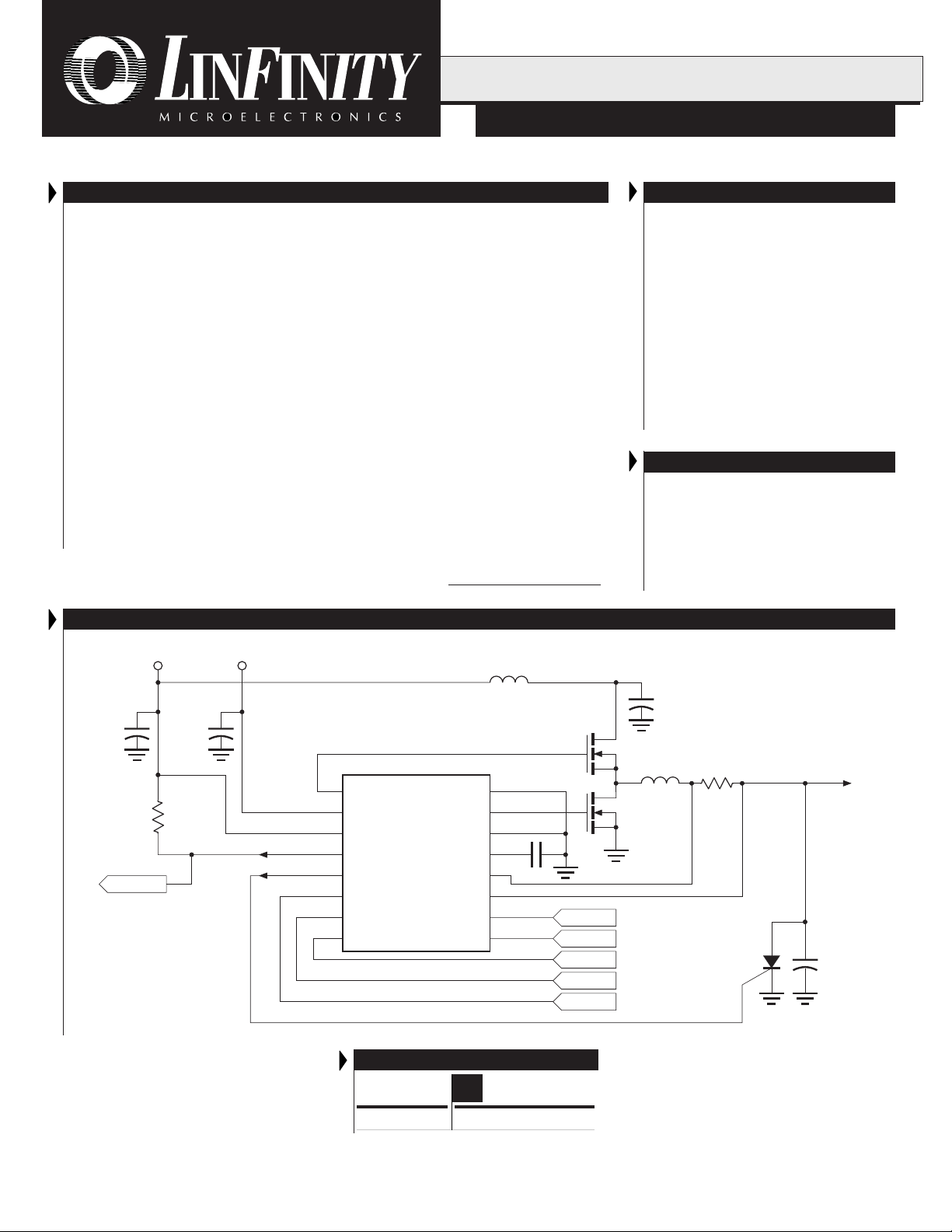
* Q4 optional OVP crowbar
1669
LX1669
P ROGRAMMABLE DC:DC CONTROLLER
T HE I NFINITE P OWER OF I NNOVATION
DESCRIPTION KEY FEATURES
The LX1669 is a Monolithic Switching
Regulator Controller IC designed to
provide a low cost, high performance
adjustable power supply for advanced
microprocessors and other applications
requiring a very fast transient response
and a high degree of accuracy. It provides
a programmable switching regulator output suitable for powering Pentium
®
II and
other processors.
Programmable Synchronous Recti-
fier Driver for CPU Core. The main
output is adjustable from 1.3 to 3.5V using
a TTL-compatible 5-bit digital code to
meet Intel specifications. The IC can read
the signal from a DIP-switch, hardwired to
Pentium II processor’s pins or from software. The 5-bit code adjusts the output
voltage between 1.30 and 2.05V in 50mV
increments, and between 2.0 and 3.5V in
NOTE: For current data & package dimensions, visit our web site: http://www.linfinity.com.
100mV increments. The device can drive
dual MOSFET’s resulting in typical efficiencies of 85 – 90%, even with loads in
excess of 10A.
Short-circuit Current Limiting with-
out Expensive Current Sense Resistors. The current sensing mechanism can
use a PCB trace resistance or the parasitic
resistance of the main inductor. For
applications requiring a high degree of
accuracy, a conventional sense resistor
can be used.
Ultra-Fast Transient Response Re-
duces System Cost. The fixed frequency
modulated off-time architecture results in
the fastest transient response for a given
inductor.
Small Package Size. The LX1669 is
available in an economical 16-pin narrow
body SOIC package.
P RODUCTION DATA SHEET
■ 5-Bit Programmable Output For CPU Core
Supply
■ Power Solution For Pentium II Processors
■ No Sense Resistor Required For Short-Circuit
Current Limiting
■ Soft-Start And Hiccup-Mode Current
Limiting Functions
■ Modulated Constant Off-Time Control
Mechanism For Fast Transient Response And
Simple System Design
■ Power Good Flag
■ Over-Voltage Pin Can Drive SCR Crowbar Or
Turn Off Signal Silver-Box Power Supply
■ Digital-Compatible Inputs (Including VID Pins)
APPLICATIONS
■ Socket 7 Processor Supplies
■ Pentium II Processor Supplies
■ Deschutes CPU & L2-Cache Memory
Supplies
■ Voltage Regulator Modules
■ General Purpose And Microprocessor
DC:DC Supplies
Copyright © 1999
Rev. 1.0 4/99
PRODUCT HIGHLIGHT
Note: All surface-mount packages are available in Tape & Reel, append the letter "T" to part number. (i.e. LX1669CDT)
L INF INITY MICROELECTRONICS INC.
11861 WESTERN AVENUE, GARDEN GROVE, CA. 92841, 714-898-8121, FAX: 714-893-2570
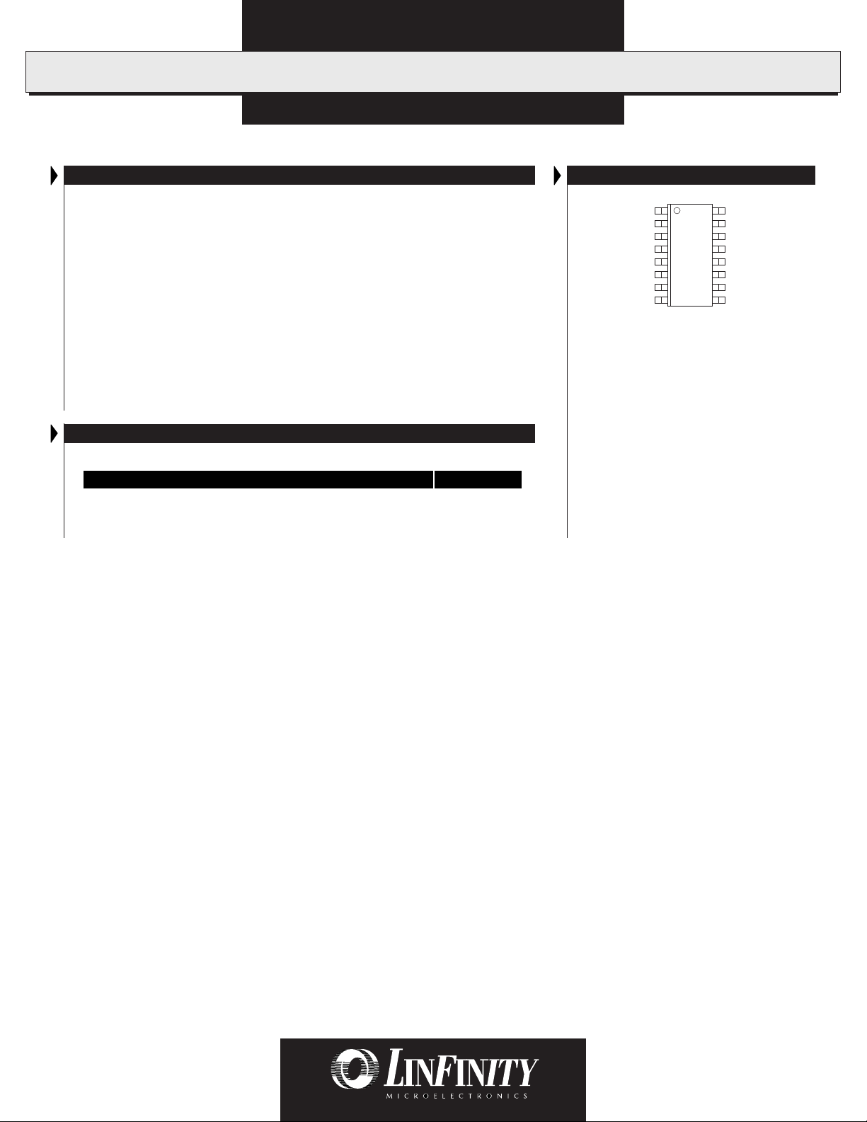
PACKAGE ORDER INFO
(°C)
T
A
0 to 70 LX1669CD
D
Plastic SOIC
16-pin
1
Page 2
LX1669
PRODUCT DATABOOK 1996/1997
P ROGRAMMABLE DC:DC CONTROLLER
RODUCTION DATA SHEET
P
ABSOLUTE MAXIMUM RATINGS (Note 1 & 2)
12V Supply Voltage (V
5V Supply Voltage (V
Output Drive Peak Current Source (500ns)....................................................... 1.0A
) .................................................................................. 18V
CC12
) ....................................................................................... 7V
CC5
Output Drive Peak Current Sink (500ns) ........................................................... 1.0A
Input Voltage (SS, VID[0:4]) ................................................................... -0.3V to 6V
Operating Junction Temperature .................................................................... 150°C
Storage Temperature Range ........................................................... -65°C to +150°C
Lead Temperature (Soldering, 10 Seconds) .................................................... 300°C
Note 1. Exceeding these ratings could cause damage to the device. All voltages are with
Note 2. V
respect to Ground. Currents are positive into, negative out of the specified
terminal.
supply is used as input to internal low dropout regulator. Voltages above
CC3
3.3V will cause increased thermal dissipation in the package. Power dissipation
should be limited to keep junction temperature below maximum rating.
THERMAL DATA
D PACKAGE:
D
x θ
θθ
θ
θθ
JA
).
JA
120°C/W
THERMAL RESISTANCE-JUNCTION TO AMBIENT,
Junction Temperature Calculation: TJ = TA + (P
The θ
numbers are guidelines for the thermal performance of the device/pc-board
JA
system. All of the above assume no ambient airflow.
PACKAGE PIN OUTS
TDRV
V
CC12
V
PWRGD
OVP
VID0
VID1
VID2
1 16
215
314
CC5
413
512
611
710
89
D PACKAGE
(Top View)
PGND
BDRV
AGND
SS/ENABLE
V
FB
V
CORE
VID4
VID3
2
Copyright © 1999
Rev. 1.0 4/99
Page 3
PRODUCT DATABOOK 1996/1997
P ROGRAMMABLE DC:DC CONTROLLER
P RODUCTION DATA SHEET
ELECTRICAL CHARACTERISTICS
(
Unless otherwise specified, 4.75V < V
Parameter
Reference & DAC
Initial Accuracy V
Cumulative Regulation Accuracy 1.3V ≤ V
Timing
Off Time OT V
Switching Frequency Freq V
Error Comparator / CS-
Input Bias Current I
E
Delay to Output Overdrive ≤ 5mV
C
Current Sense +
Input Resistance R
Pulse By Pulse Current Limit V
Current Sense Delay To Output Overdrive ≤ 5mV
Output Drivers
Drive Rise Time, Fall Time T
Drive High V
Drive Low V
UVLO and Soft-Start (SS)
V
Start-Up Threshold V
CC5
Hysteresis
SS Resistor R
SS Output Enable V
Hiccup Duty Cycle DC
Supply Current
V
Dynamic Supply Current I
CC12
Static Supply Current 12V I
5V I
Power Good / Over-Voltage Protection (OVP)
Threshold (V
Hysteresis
Power Good Voltage Low I
Over-Voltage Threshold (V
OVP Sourcing Current V
VID Pins
Low Input VILInternally pulled up to V
High Input V
< 5.25V and 10.8V < V
CC5
Symbol
(Less 40mV output adaptive positioning)
CORE
= 2.0V
CORE
= 1.3V to 3.5V
CORE
1.0V < VSS = VFB < 3.5V
FB
0V < VFB = V
CORE
CLP
CL = 3000pF
RF
DHISOURCE
DLISINK
STVCC12
SS
EN
HICCSS
CD
VCC12VSS
VCC5VSS
IH
= 20mA
> 3.9V
= 0.1µF, V
Out Freq = 200kHz, CL = 3000pF, Synch., VSS > 0.5V
< 0.5V
< 0.5V
CORE
(V
CORE
= 4mA
PWRGD
CORE
= 2.0V
OVP
≤ 3.5V
CORE
CORE
= 20mA
/ V
) V
SET
/ V
) V
SET
/ V
), V
SET
< 13.2V, 0°C ≤ TA ≤ 70°C. Test conditions: V
CC12
Test Conditions
< 3.5V
= 2.00V, F
DAC
rising, V
CORE
falling, V
CORE
rising
CORE
= 100Hz
REQ
OUT2
OUT2
thru 30k
CC5
, 1.3V ≤ V
≥ 2.0V
≥ 2.0V
≤ 3.5V, T
CORE
= 25°C
A
LX1669
= 5V, V
CC5
Min. Typ. Max.
-1 +1 %
-1.5 1.5 %
45 60 mV
10 11 V
3.9 4.2 4.6 V
0.4 0.5 V
108 110 111 %
90 91 92 %
110 117 125 %
35 60 mA
2.0 V
= 12V, T = 25°C.
CC12
LX1669
2.4 µs
250 kHz
-0.3 -1 µ A
100 ns
12 kΩ
100 ns
100 ns
0.1 0.2 V
0.10 V
18 kΩ
10 %
24 mA
69mA
13 18 mA
2%
0.5 0.7 V
0.8 V
)
Units
Copyright © 1999
Rev. 1.0 4/99
3
Page 4
LX1669
PRODUCT DATABOOK 1996/1997
P ROGRAMMABLE DC:DC CONTROLLER
RODUCTION DATA SHEET
P
ELECTRICAL CHARACTERISTICS
Table 1 - Adaptive Transient Voltage Output (Output Voltage Setpoint — Typical)
Processor Pins
0 = Low, 1 = High
VID4 VID3 VID2 VID1 VID0
011111.34V 1.30V
011101.39V 1.35V
011011.44V 1.40V
011001.49V 1.45V
010111.54V 1.50V
010101.59V 1.55V
010011.64V 1.60V
010001.69V 1.65V
001111.74V 1.70V
001101.79V 1.75V
001011.84V 1.80V
001001.89V 1.85V
000111.94V 1.90V
000101.99V 1.95V
000012.04V 2.00V
000002.09V 2.05V
111112.04V 2.00V
111102.14V 2.10V
111012.24V 2.20V
111002.34V 2.30V
110112.44V 2.40V
110102.54V 2.50V
110012.64V 2.60V
110002.74V 2.70V
101112.84V 2.80V
101102.94V 2.90V
101013.04V 3.00V
101003.14V 3.10V
100113.24V 3.20V
100103.34V 3.30V
100013.44V 3.40V
100003.54V 3.50V
* Nominal = DAC setpoint voltage with no adaptive output voltage positioning.
Output Voltage (V
0.0A
Nominal Output* (V
SET
)
)
SET
Note:
Adaptive Transient Voltage Output
In order to improve transient response a 40mV offset is built into the voltage comparator. At high currents, the
peak output voltage will be lower than the nominal set point , as shown in Figure 4. The actual output voltage
will be a function of the sense resistor, output current and output ripple.
4
Copyright © 1999
Rev. 1.0 4/99
Page 5
PRODUCT DATABOOK 1996/1997
V
P ROGRAMMABLE DC:DC CONTROLLER
P RODUCTION DATA SHEET
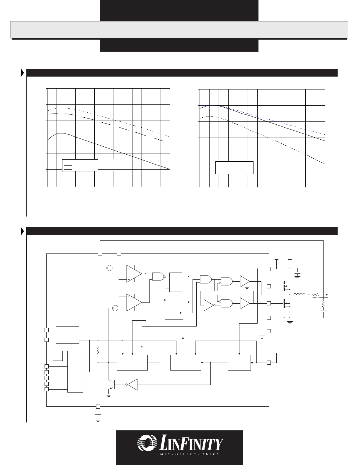
CHARACTERISTICS CURVES
LX1669
100
95
90
85
EFFICIENCY (%)__
80
EFFICIENCY A T 3. 1V
EFFICIENCY A T 2. 8V
75
70
123456 7891011121314
EFFICIENCY A T 1. 8V
I
OUT
(A)
FIGURE 1 — Efficiency Test Results:
V
FB
CS Comp
Error Comp
Hiccup
= 5V
IN
I
PWRGD
OVP
ID[0:4]
Non-Synchronous Operation, V
4
Power Good
& OVP
5
V
REF
6
7
8
9
10
DAC
V
SET
V
CORE
R
20k
12
60mV
40mV
SS
11
100
95
90
85
EFFICIENCY (%)__
80
75
70
BLOCK DIAGRAM
RESET
V
RESET
Hiccup
R
SQ
Set
PWM
Q
Off-Time
Control
EFFICIENCY AT 3.1V
EFFICIENCY A T 2.8V
EFFICIENCY A T 1.8V
1234567891011121314
I
(A)
OUT
FIGURE 2 — Efficiency Test Results:
Synchronous Operation, VIN = 5V
+12V
VIN (5V)
2
V
UVLO
UVLO
15
16
14
1
3
CC12
TDRV
BDRV
PGND
AGND
+5V
V
CC5
C
IN
R
SENSE
L
V
ESR
C
OUT
CORE
SS/ENABLE
Copyright © 1999
Rev. 1.0 4/99
13
C
SS
FIGURE 3 — Block Diagram
5
Page 6

LX1669
Pin Pin
Number Designator Description
1 TDRV Gate drive to the top FET.
2V
3V
CC12
CC5
4 PWRGD Open collector output, pulled down when the core voltage is not within ±10% of the DAC output.
5 OVP Over-voltage protection: this pin is pulled to above 3V when the switcher output is above 17% of its set
6 VID0 Input pins to the DAC. The output of the DAC sets the nominal voltage of the PWM output (see Table 1).
7 VID1 These inputs are TTL-compatible.
8 VID2
9 VID3
10 VID4
11 V
12 V
CORE
FB
13 SS/ENABLE Soft-startup and hiccup capacitor pin. During startup, the voltage of this pin controls the core voltage. An
14 AGND Analog ground.
15 BDRV Bottom FET drive.
16 PGND Power ground. Ground return for FET drivers.
+12V supply for the gate drivers. If 12V is not available in the application, a bootstrap circuit is required
to create the biasing voltage for the FET gate drivers.
+5V supply for internal biasing and power to the IC.
voltage. This pin is capable of sourcing 40mA current, and can be used to drive an SCR crowbar or as a
signal to turn off the main power supply.
Output (CPU core) voltage, connected to the output of the regulator (after the sense resistor). This pin is
also connected to the power good and the over current comparators in the IC.
Dual function pin for feedback and current sensing. The peak voltage of this is set 40mV above the
nominal set-point (VID) voltage. When the voltage difference between this pin and V
60mV, the over current comparator will be tripped. The over current tripping level can be set as
I = 60mV/R
internal 20kΩ resistor and the external capacitor set the time constant for the soft-startup. Soft-start does
not begin until the supply voltage exceeds the UVLO threshold. When over-current occurs, this capacitor is
used for timing the hiccup. See Application Information for more detail. The PWM output can be disabled
by pulling the SS/ENABLE pin below 0.5V.
PRODUCT DATABOOK 1996/1997
P ROGRAMMABLE DC:DC CONTROLLER
RODUCTION DATA SHEET
P
FUNCTIONAL PIN DESCRIPTION
SENSE
where R
is the sensing resistance (see Application Note section).
SENSE
(pin 15) exceeds
OUT
6
Copyright © 1999
Rev. 1.0 4/99
Page 7

PRODUCT DATABOOK 1996/1997
P ROGRAMMABLE DC:DC CONTROLLER
P RODUCTION DATA SHEET
THEORY OF OPERATION
LX1669
SWITCHER OUTPUT VOLTAGE REGULATION
Refer to the IC Block Diagram and the Product Highlight circuit.
When the top MOSFET turns ON, the inductor current increases.
The voltage at V
capacitor and the current-sensing resistor. When the V
voltage reaches the threshold voltage of the error comparator,
(the DAC output set-point voltage) plus 40mV offset, the
V
SET
PWM latch is reset. Consequently, the top MOSFET turns OFF
pin increases due to the ESR of the output
FB
FB
pin
and the bottom (synchronous) MOSFET turns ON. The off-time
control block controls the off-time of the top MOSFET. During
the off-time, the inductor current and the V
decrease. As the off-time finishes, the synchronous MOSFET
pin voltage
FB
turns OFF and the top MOSFET turns ON again, repeating the
previous cycle. A break-before-make circuit prevents simultaneous conduction of the two MOSFET’s.
The 40mV offset to the set voltage enhances the transient
response of the output voltage, as shown in Figure 4 below.
■ The peak voltage at the V
voltage and its average is the peak voltage minus the ripple
voltage at V
■ The output voltage is the voltage at the V
FB
pin.
voltage drop across the current sensing resistor (I * R
■ At light loads, the voltage drop across the sensing resistor
pin is 40mV higher than the set
FB
pin minus the
FB
SENSE
is small; hence, the output voltage is approximately the
voltage at the V
set voltage, V
■ At heavy loads, larger current flows in the sense resistor,
pin (approximately 40mV higher than the
FB
).
SET
therefore, the voltage drop is higher and the output voltage
is lower.
This adaptive positioning of the output voltage as the load
changes allows a greater output voltage excursion during a fast
step-load transient and requires fewer output capacitors to meet
the transient-response specification.
POWER UP and INITIALIZATION
At power up, the LX1669 monitors the supply voltage to both the
+5V and the +12V pins (there is no special requirement for the
sequence of the two supplies). Before both supplies reach their
under-voltage lock-out (UVLO) thresholds, the soft-start (SS) pin
is held low to prevent soft-start from beginning; the off-time
control is disabled and the top MOSFET is kept OFF. After both
supplies pass the UVLO thresholds, the circuit begins soft-start.
SOFT-START
Once the supplies are above the UVLO threshold, the soft-start
capacitor begins to be charged up by the set voltage (DAC
output) through a 20kΩ internal resistor. The capacitor voltage
at the SS pin rises as a simple RC circuit. The SS pin plus a 40mV
offset is connected to the error comparator’s non-inverting input
that controls the output peak voltage. The output voltage will
follow the SS pin voltage if sufficient charging current is provided
to the output capacitor.
The simple RC soft-start allows the output to rise faster at the
beginning and slower at the end of the soft-start interval. Thus,
the required charging current into the output capacitor is less at
the end of the soft-start interval so decreasing the possibility of
).
an over-current. A comparator monitors the SS pin voltage and
indicates the end of soft-start when SS pin voltage reaches 95%
of V
. See Application Information section for further details.
SET
of the load current step and
Copyright © 1999
Rev. 1.0 4/99
Adaptive voltage
positioning offset
(40mV)
V
OFFSET
Nominal set-point
voltage, V
Dynamic voltage tolerance
(100mV for 2µs)
V
DYN
Initial voltage drop is
mainly due to the product
ESR of the capacitors.
(ESL effects are ignored)
(2.0V)
SET
∆V = ∆I * ESR
L
= 2.5µH, C
OUT
= 6x1500µF Sanyo MV-GX, R
OUT
SENSE
FIGURE 4 — Adaptive Voltage Positioning
= 2.5mΩ
Output voltage
(50mV/Div)
V
OUT
Steady state voltage at high
current is approximately
V
+ V
- I
SET
OFFSET
Output current transient
step, ∆I = 0 to 14A
(5A/Div)
OUT
x R
SENSE
7
Page 8

LX1669
PRODUCT DATABOOK 1996/1997
P ROGRAMMABLE DC:DC CONTROLLER
RODUCTION DATA SHEET
P
THEORY OF OPERATION
OVER-CURRENT PROTECTION (OCP) and HICCUP
The over-current protection function is tripped when the inductor current exceeds its maximum limit. The current is sensed
with a resistor in series with the inductor. When the voltage
across the sensing resistor exceeds the 60mV threshold, the OCP
comparator outputs a signal to reset the PWM latch and to start
hiccup mode. The soft-start capacitor, C
(10 times slower than when being charged up by R
voltage on the SS/ENABLE pin reaches a 0.3V threshold, hiccup
, is discharged slowly
SS
). When the
SS
finishes and the circuit soft-starts again. During hiccup, the top
MOSFET is OFF and the bottom MOSFET remains ON.
Hiccup is disabled during the soft-start interval, allowing the
circuit to start up with the maximum current. If the rise speed
of the output voltage is too fast, the required charging current to
the output capacitor may be higher than the limit-current. In this
case, the peak inductor current is regulated to the limit-current
by the current-sense comparator. The top MOSFET is turned on
at the end of the controlled off-time and is turned off when the
inductor current reaches the limit. If the inductor current still
reaches its limit after the soft-start finishes, the hiccup is triggered
again. The hiccup ensures the average heat generation on both
MOSFET’s and the average current to be much less than that in
normal operation, if the output has a short circuit.
OVER-VOLTAGE PROTECTION (OVP)
The output voltage is inherently protected from an over-voltage
situation because of the peak-voltage control mechanism.
Whenever the V
40mV, the top MOSFET is turned off and the bottom MOSFET is
pin voltage is higher than the set voltage by
FB
turned on. In the case that a fault condition occurs where the
OVER-VOLTAGE PROTECTION (OVP) (continued)
output voltage exceeds the 117% V
comparator will pull up the OVP pin to 2 volts. The OVP pin has
threshold, the OVP
SET
a 40mA source current capability, so it can be used to trigger an
SCR crowbar or shut off the main power supply.
OFF-TIME CONTROL and SWITCHING FREQUENCY
An internal timer controls the off-time of the top MOSFET so that
the switching frequency is constant at 250kHz under steady-state
operation. The timer begins timing once the PWM latch is reset
and set the PWM flip-flop again when the off-time finishes. The
off-time is controlled to be:
T
= 4µs(1-V
OFF
OUT /VCC5
)
For a buck converter, the switching frequency is
f
= (1- V
SW
OUT /VCC5
)/T
OFF
Therefore, the switching frequency is nearly constant in steady
state operation. During transient loading, the top drive can
remain switched on or off until the output voltage is within
specification (see Figure 5) in order to reduce transient response
time.
POWER GOOD OUTPUT
An open-collector output, PWRGD, is provided to indicate the
status of the output voltages. PWRGD presents high impedance
when the switcher output voltage is within ±10% of its set
voltage. Otherwise, PWRGD presents a low impedance path to
ground.
Top FET Drive
Output Voltage
(2.8V Set Point)
13A Load Transient
(in 390ns)
VIN = 5V, V
= 2.8V, L
OUT
= 5µH, C
OUT
= 3 x 1500µF, f = 200kHz
OUT
FIGURE 5 — Top FET Drive During Transient Load Conditions
8
Copyright © 1999
Rev. 1.0 4/99
Page 9

PRODUCT DATABOOK 1996/1997
LX1669
P ROGRAMMABLE DC:DC CONTROLLER
P RODUCTION DATA SHEET
BILL OF MATERIALS
LX1669 Bill of Materials (Refer to Product Highlight)
Ref Description Part Number / Manufacturer Qty.
U1 Controller IC LX1668 - LinFinity 1
C1 Capacitor, 1500µF, 6.3V, 44mΩ ESR MV-GX Sanyo 6
C2 Capacitor, 1500µF, 6.3V, 44mΩ ESR MV-GX Sanyo 3
C8 Capacitor, 1µF, SMD 2
C3 Capacitor, 1µF, SMD, 16V 1
CSS Capacitor, 0.1µF, SMD 1
Q1 MOSFET (low R
Q2 MOSFET (low R
R
SENSE
L1 Inductor, 2 - 3µH HM00-97713 or HM00-98637, BI Technologies 1
L2 Inductor, 1µH 1
Total Number of Components 19
Optional Components for Over-Voltage Protection and Power Good Signal
Q4 SCR 2N6504 1
R3 Resistor, 10kΩ SMD 1
Sense Resistor, 2.5mΩ PCB trace 1
) IRL3102/3103, International Rectifier 1
DS(ON)
) IRL3303/3103, International Rectifier 1
DS(ON)
Copyright © 1999
Rev. 1.0 4/99
9
Page 10

LX1669
PRODUCT DATABOOK 1996/1997
P ROGRAMMABLE DC:DC CONTROLLER
RODUCTION DATA SHEET
P
APPLICATION INFORMATION
Output Voltage
(2.8V Set Point)
Input Ripple Voltage
Input Current
L
= 5µH, LIN = 0
OUT
L
= 2.2µH, LIN = 0
OUT
FIGURE 6 — Effect Of Different Inductor Values
OUTPUT INDUCTOR
The output inductor should be selected to meet the requirements
of the output voltage ripple in steady-state operation and the
inductor current slew-rate during transient.
The peak-to-peak output voltage ripple is:
= ESR * I
V
RIPPLE
RIPPLE
where
(V
- V
)
IN
= *
I
RIPPLE
is the inductor ripple current, L is the output inductor
I
RIPPLE
value and ESR is the Effective Series Resistance of the output
OUT
* L
f
SW
V
OUT
V
IN
capacitor.
I
should typically be in the range of 20% to 40% of the
RIPPLE
maximum output current. Higher inductance results in lower
output voltage ripple, allowing slightly higher ESR to satisfy the
transient specification. Higher inductance also slows the inductor current slew rate in response to the load-current step change,
∆I, resulting in more output-capacitor voltage droop. The
inductor-current rise and fall times are:
T
= L * ∆I/(VIN – V
RISE
OUT
)
and
= L * ∆I/V
T
FALL
OUT
When using electrolytic capacitors, the capacitor voltage
droop is usually negligible, due to the large capacitance.
For higher current applications, such as Pentium II processors, a 2.5µH inductor is recommended for the best combination
of fast response and manageable ripple voltage. For lower
current applications, such as Pentium and other Socket 7
processors, a 5µH inductor is sufficient. The effect of different
inductor values is shown in Figure 6 above.
Notice how, with a smaller inductor, transient response time
is improved, but at the expense of much greater ripple.
INPUT INDUCTOR
In order to supply faster transient load changes, a smaller output
inductor is needed. However, reducing the size of the output
inductor will result in a higher ripple voltage on the input supply,
as shown in Figure 6 above. This noise on the 5V rail can affect
other system components, such as graphics cards. It is recommended that a 1 – 1.5µH inductor, L2, is used on input to the
regulator, to filter the ripple on the 5V supply. Ensure that this
inductor has the same current rating as the output inductor.
OUTPUT CAPACITOR
The output capacitor is sized to meet ripple and transient
performance specifications. Effective Series Resistance (ESR) is
a critical parameter. When a step load current occurs, the output
voltage will have a step that equals the product of the ESR and
the current step, ∆I. In an advanced microprocessor power
supply, the output capacitor is usually selected for ESR instead
of capacitance or RMS current capability. A capacitor that
satisfies the ESR requirement usually has a larger capacitance and
current capability than strictly needed. The allowed ESR can be
found by:
ESR * (I
where I
load current step change, and V
RIPPLE
+ ∆I ) < V
RIPPLE
EX
is the inductor ripple current, ∆I is the maximum
is the allowed output voltage
EX
10
Copyright © 1999
Rev. 1.0 4/99
Page 11

PRODUCT DATABOOK 1996/1997
P ROGRAMMABLE DC:DC CONTROLLER
P RODUCTION DATA SHEET
APPLICATION INFORMATION
LX1669
OUTPUT CAPACITOR (continued)
excursion in the transient. Adaptive voltage positioning increases the value of V
reducing the cost of the output capacitor. The positioning
, allowing a higher ESR value and
EX
voltage is 40mV (peak), using the LX1669, and the transient
tolerance is 100mV, resulting in a V
Electrolytic capacitors can be used for the output capacitor,
of 140mV (see Figure 4).
EX
but are less stable with age than tantalum capacitors. As they age,
their ESR degrades, reducing the system performance and
increasing the risk of failure. It is recommended that multiple
parallel capacitors be used, so that, as ESR increases with age,
overall performance will still meet the processor’s requirements.
There is frequently strong pressure to use the least expensive
components possible, however, this could lead to degraded
long-term reliability, especially in the case of filter capacitors.
Linfinity’s demonstration boards use Sanyo MV-GX filter capacitors, which are aluminum electrolytic, and have demonstrated
reliability. The Oscon series from Sanyo generally provides the
very best performance in terms of long term ESR stability and
general reliability, but at a substantial cost penalty. The MV-GX
series provides excellent ESR performance at a reasonable cost.
Beware of off-brand, very low-cost filter capacitors, which have
been shown to degrade in both ESR and general electrolytic
characteristics over time.
INPUT CAPACITOR
The input capacitor and the input inductor are to filter the
pulsating current generated by the buck converter to reduce
interference to other circuits connected to the same 5V rail. In
addition, the input capacitor provides local de-coupling the buck
converter. The capacitor should be rated to handle the RMS
current requirement. The RMS current is:
I
= IL √ d(1-d)
RMS
where I
maximum value, when d = 50%, I
output in the range of 2 to 3V, the required RMS current is very
close to 0.5I
is the inductor current and the d is the duty cycle. The
L
.
A high-frequency (ceramic) capacitor should be placed
L
= 0.5IL. For 5V input and
RMS
across the drain of the top MOSFET and the source of the bottom
one to avoid ringing due to the parasitic inductor being switched
ON and OFF. See capacitor C7 in the Product Highlight.
SOFT-START CAPACITOR
The value of the soft-start capacitor determines how fast the
output voltage rises and how large the inductor current is
required to charge the output capacitor. The output voltage will
follow the voltage at SS pin if the required inductor current does
not exceed the maximum current in the inductor.
SOFT-START CAPACITOR
(continued)
The SS pin voltage can be expressed as:
-t/RssC
= V
V
SS
where V
resistor and capacitor, as shown in Figure 3. The required
(1-e
SET
is the output of the DAC. RSS and CSS are soft start
SET
ss
)
inductor current for the output capacitor to follow the SS-pin
voltage equals the required capacitor current plus the load
current. The soft-start capacitor should be selected so that the
overall inductor current does not exceed it maximum.
The capacitor current to follow the SS-pin voltage is:
I
= C
Cout
where C
C
should be in the range of 0.1 to 0.2µF.
SS
During the soft-start interval, before the PWRGD signal
dV
OUT
dt
is the output capacitance. The typical value of
OUT
C
OUT
=* e
-(t/RssCss)
C
SS
becomes valid, the load current from a microprocessor is
negligible; therefore, the capacitor current is approximately the
required inductor current.
CURRENT LIMIT
Current limiting occurs when a sensed voltage, proportional to
load current, exceeds the current-sense comparator threshold
value. The current can be sensed either by using a fixed sense
resistor in series with the inductor to cause a voltage drop
proportional to current, or by using a resistor and capacitor in
parallel with the inductor to sense the voltage drop across the
parasitic resistance of the inductor. The LX1669 has a threshold
of 60mV.
Sense Resistor
The current sense resistor, R
formula:
R
= V
/ I
TRIP
TRIP
is the current sense comparator threshold (60mV)
TRIP
Where V
and I
below.
SENSE
is the desired current limit. Typical choices are shown
TRIP
, is selected according to the
SENSE
TABLE 2 - Current Sense Resistor Selection Guide
Sense Resistor
Load Value
Pentium-Class Processor (<10A) 5mΩ
Pentium II Class (>10A) 2.5mΩ
A smaller sense resistor will result in lower heat dissipation
(I²R) and also a smaller output voltage droop at higher currents.
Copyright © 1999
Rev. 1.0 4/99
11
Page 12

PRODUCT DATABOOK 1996/1997
LX1669
P ROGRAMMABLE DC:DC CONTROLLER
RODUCTION DATA SHEET
P
APPLICATION INFORMATION
CURRENT LIMIT (continued)
There are several alternative types of sense resistor. The
surface-mount metal “staple” form of resistor has the advantage of
exposure to free air to dissipate heat and its value can be
controlled very tightly. Its main drawback, however, is cost. An
alternative is to construct the sense resistor using a copper PCB
trace. Although the resistance cannot be controlled as tightly, the
PCB trace is very low cost.
L
R
L
Load
R
S
C
S
PCB Sense Resistor
A PCB sense resistor should be constructed as shown in Figure 7.
By attaching directly to the large pads for the capacitor and
inductor, heat is dissipated efficiently by the larger copper masses.
Connect the current sense lines as shown to avoid any errors.
Inductor
2.5mΩ
100mil Wide, 850mil Long
2.5mm x 22mm (2 oz/ft
Sense Resistor
2
copper)
Output
Capacitor Pad
Sense Lines
FIGURE 7 — Sense Resistor Construction Diagram
Recommended sense resistor sizes are given in the following
table:
TABLE 3 - PCB Sense Resistor Selection Guide
Copper Copper Desired Resistor Dimensions (w x l)
Weight Thickness Value mm inches
2
2 oz/ft
68µm 2.5m
5m
Ω
Ω
2.5 x 22 0.1 x 0.85
2.5 x 43 0.1 x 1.7
Current
Sense
R
S2
V
CS
Comparator
FIGURE 8 — Current Sense Circuit
The voltage across the capacitor will be equal to the current
flowing through the resistor, i.e.
= ILR
V
CS
L
Since VCS reflects the inductor current, by selecting the
appropriate R
and CS, VCS can used to sense current.
S
Design Example
(Pentium II circuit, with a maximum static current of 14.2A)
The gain of the sensor can be characterized as:
|T(jω)|
R
L
L/RSC
S
ω
1/R
SCSRL
FIGURE 9 — Sensor Gain
/L
Loss-Less Current Sensing Using Resistance of Inductor
Any inductor has a parasitic resistance (RL) which causes a DC
voltage drop when current flows through the inductor. Figure 8
shows a sensor circuit comprising of a surface mount resistor, R
and capacitor, C
current sense resistor.
in parallel with the inductor, eliminating the
S,
The current flowing through the inductor is a triangle wave. If
the sensor components are selected such that:
= RS * C
L/R
L
S
12
The dc/static tripping current I
V
trip
=
I
,
S
trip,S
Select L/R
the static one. The dynamic tripping current I
I
trip,d
R
L
≤ RL to have higher dynamic tripping current than
SCS
V
trip
=
L/(RSCS )
trip,S
satisfies:
satisfies:
trip,d
Copyright © 1999
Rev. 1.0 4/99
Page 13

PRODUCT DATABOOK 1996/1997
P ROGRAMMABLE DC:DC CONTROLLER
P RODUCTION DATA SHEET
APPLICATION INFORMATION
LX1669
CURRENT LIMIT (continued)
General Guidelines for Selecting RS , CS, and R
V
trip
RL = Select: R
I
trip,S
according to: CSn =
and C
S
≤ 10 kΩ
S
L
n
RL R
S
L
The above equation has taken into account the currentdependency of the inductance.
Typical values are: R
2.5µH at 0A current.
In cases where R
be lower than the desired short-circuit current limit, a resistor (R
can be put in parallel with C
of components is as follows:
R
L (Required)
R
L (Actual)
C
= =
S
R
L (Actual)
Again, select (R
more information.
= 3mΩ, RS = 9kΩ, C
L
is so large that the trip point current would
L
, as shown in Figure 9. The selection
S
R
S2
=
RS2 + R
S
L
(RS2 // RS )LR
*
//R
) < 10kΩ. See Application Note AN-7 for
S2
S
L (Actual)
= 0.1µF, and L is
S
RS + R
RS2 * R
S2
S
*
S2
OUTPUT ENABLE
The LX1669 FET driver outputs are driven to ground by pulling
the soft-start pin below 0.5V.
PROGRAMMING THE OUTPUT VOLTAGE
The output voltage is set by the DAC with a 5-bit digital voltageidentification (VID) code input (see Table 1). The DAC input is
designed to be compatible with digital circuits. The VID code
may be hard-wired into the package of the processor [as in the
case of a Pentium II or Pentium Pro processor]. If the processor
does not have a VID code, the output voltage can be set by
means of a DIP-switch, jumpers or TTL-compatible digital
circuits. When using a DIP-switch or jumpers, connect the VID
pin to ground (DIP-switch ON) for a low or “0” signal and leave
the VID pin open (DIP-switch OFF) for a high or “1” signal.
FET SELECTION
To insure reliable operation, the operating junction temperature
of the FET switches must be kept below certain limits. The Intel
specification states that 115°C maximum junction temperature
should be maintained with an ambient of 50°C. This is achieved
by properly derating the part, and by adequate heat sinking. One
of the most critical parameters for FET selection is the R
resistance. This parameter directly contributes to the power
DS(ON)
dissipation of the FET devices, and thus impacts heat sink design,
mechanical layout, and reliability. In general, the larger the
current handling capability of the FET, the lower the R
be, since more die area is available.
DS(ON)
will
FET SELECTION (continued)
TABLE 4 - FET Selection Guide
This table gives selection of suitable FETs from International Rectifier.
Device R
@I
DS(ON)
ΩΩ
10V (m
Ω)T
ΩΩ
@ Max. Break-
D
= 100°C down Voltage
C
IRL3803 6 83 30
IRL22203N 7 71 30
IRL3103 14 40 30
IRL3102 13 56 20
IRL3303 26 24 30
)
IRL2703 40 17 30
All devices in TO-220 package. For surface mount devices (TO-263 /
D2-Pak), add 'S' to part number, e.g. IRL3103S.
The recommended solution is to use IRL3102 for the high side
and IRL3303 for the low side FET, for the best combination of cost
and performance. Alternative FET’s from any manufacturer could
be used, provided they meet the same criteria for R
Heat Dissipated In Upper MOSFET
The heat dissipated in the top MOSFET will be:
= (I2 * R
P
D
Where t
and f
S
For the IRL3102 (13mΩ R
is switching transition line for body diode (~100ns)
SW
is the switching frequency.
will result in typical heat dissipation of 1.92W.
* Duty Cycle) + (0.5 * I * VIN * tSW * fS )
DS(ON)
), converting 5V to 2.0V at 15A
DS(ON)
Synchronous Rectification – Lower MOSFET
The lower pass element can be either a MOSFET or a Schottky
diode. The use of a MOSFET (synchronous rectification) will result
in higher efficiency, but at higher cost than using a Schottky diode
(non-synchronous).
Power dissipated in the bottom MOSFET will be:
P
= I2 * R
D
[IRL3303 or 1.76W for the IRL3102]
* [1 - Duty Cycle] = 3.51W
DS(ON)
Non-Synchronous Operation - Schottky Diode
A typical Schottky diode with a forward drop of 0.6V will dissipate
0.6 x 15 * (1-2/5) = 5.4W (compared to the 1.8 to 3.5W dissipated
by a MOSFET under the same conditions). This power loss
becomes much more significant at lower duty cycles – synchronous rectification is recommended. The use of a dual Schottky
diode in a single TO-220 package (e.g. the MBR2535) helps
improve thermal dissipation.
DS(ON)
.
Copyright © 1999
Rev. 1.0 4/99
13
Page 14

PRODUCT DATABOOK 1996/1997
t
LX1669
P ROGRAMMABLE DC:DC CONTROLLER
RODUCTION DATA SHEET
P
APPLICATION INFORMATION
LAYOUT GUIDELINES - THERMAL DESIGN
A great deal of time and effort were spent optimizing the thermal
design of the demonstration boards. Any user who intends to
implement an embedded motherboard would be well advised to
carefully read and follow these guidelines. If the FET switches
have been carefully selected, external heatsinking is generally not
required. However, this means that copper trace on the PC board
must now be used. This is a potential trouble spot;
copper area as possible must be dedicated to heatsinking the FET
switches, and the diode as well if a non-synchronous solution is
used.
In our demonstration board, heatsink area was taken from
internal ground and V
connected with VIAS to the power device tabs. The TO-220 and
TO-263 cases are well suited for this application, and are the
preferred packages. Remember to remove any conformal coating
from all exposed PC traces which are involved in heatsinking.
planes which were actually split and
CC
5V Input
as much
LX1669
Outpu
PGND
FIGURE 10 — Power Traces
General Notes
As always, be sure to provide local capacitive decoupling close to
the chip. Be sure use ground plane construction for all highfrequency work. Use low ESR capacitors where justified, but be
alert for damping and ringing problems. High-frequency designs
demand careful routing and layout, and may require several
iterations to achieve desired performance levels.
Power Traces
To reduce power losses due to ohmic resistance, careful consideration should be given to the layout of traces that carry high
currents. The main paths to consider are:
■ Input power from 5V supply to drain of top MOSFET.
■ Trace between top MOSFET and lower MOSFET or Schottky
diode.
■ Trace between lower MOSFET or Schottky diode and ground.
■ Trace between source of top MOSFET and inductor, sense
resistor and load.
■ Current traces on both LDO sections
All of these traces should be made as wide and thick as
possible, in order to minimize resistance and hence power losses.
It is also recommended that, whenever possible, the ground, input
and output power signals should be on separate planes (PCB
layers). See Figure 10 – bold traces are power traces.
Input Decoupling Capacitors
Ensure that capacitors C8 and C3 are placed as close to the IC as
possible to minimize the effects of noise on the device.
Layout Assistance
Please contact Linfinity’s Applications Engineers for assistance
with any layout or component selection issues. A Gerber file with
layout for the most popular devices is available upon request.
Evaluation boards are also available upon request. Please
check Linfinity's web site for further application notes.
RELATED DEVICES
LX1668
Triple Output Regulator
(Programmable switching regulator with internal 2.5V
LDO plus linear regulator driver)
14
PRODUCTION DATA - Information contained in this document is proprietary to LinFinity, and is current as of publication date. This document
may not be modified in any way without the express written consent of LinFinity. Product processing does not necessarily include testing of
all parameters. Linfinity reserves the right to change the configuration and performance of the product and to discontinue product at any time.
Pentium is a registered trademark of Intel Corporation.
Copyright © 1999
Rev. 1.0 4/99
 Loading...