

Datasheet LX1665CN, LX1665CDW, LX1665ACN, LX1665ACDW, LX1664CN Datasheet (Microsemi Corporation)
...Page 1
LX1664/64A, LX1665/65A
DUAL OUTPUT PWM CONTROLLERS WITH 5-BIT DAC
T HE I NFINITE P OWER OF I NNOVATION
DESCRIPTION KEY FEATURES
The LX1664/64A and LX1665/65A are
monolithic switching regulator controller IC’s designed to provide a low cost,
high performance adjustable power supply
for advanced microprocessors and other
applications requiring a very fast transient
response and a high degree of accuracy.
Short-circuit Current Limiting with-
out Expensive Current Sense Resistors.
Current-sensing mechanism can use PCB
trace resistance or the parasitic resistance of
the main inductor. The LX1664A and
LX1665A have reduced current sense comparator threshold for optimum performance using a sense resistor. For applications requiring a high degree of accuracy, a
conventional sense resistor can be used to
sense current.
Programmable Synchronous Recti-
fier Driver for CPU Core. The main
output is adjustable from 1.3V to 3.5V using
a 5-bit code. The IC can read a VID signal
IMPORTANT: For the most current data, consult LinFinity's web site: http://www.linfinity.com.
set by a DIP switch on the motherboard, or
hardwired into the processor’s package (as
in the case of Pentium
®
Pro and Pentium II
processors). The 5-bit code adjusts the
output voltage between 1.30 and 2.05V in
50mV increments and between 2.0 and 3.5V
in 100mV increments, conforming to the
Intel Corporation specification. The device
can drive dual MOSFET’s resulting in typical
efficiencies of 85 - 90% even with loads in
excess of 10 amperes. For cost sensitive
applications, the bottom MOSFET can be
replaced with a Schottky diode (non-synchronous operation).
Linear Regulator Driver. The LX1664/
65 family of devices have a secondary
regulator output. This can drive a MOSFET
or bipolar transistor as a pass element to
construct a low-cost adjustable linear regulator suitable for powering a 1.5V GTL+ bus
or 2.5V clock supply.
(continued next page)
P RODUCTION DATA SHEET
■ 5-bit Programmable Output For CPU Core
Supply
■ Adjustable Linear Regulator Driver Output
■ No Sense Resistor Required For Short-
Circuit Current Limiting
■ Designed To Drive Either Synchronous Or
Non-Synchronous Output Stages
■ Soft-Start Capability
■ Modulated, Constant Off-Time Architecture
For Fast Transient Response And Simple
System Design
■ Available Over-Voltage Protection (OVP)
Crowbar Driver And Power Good Flag
(LX1665 only)
APPLICATIONS
■ Socket 7 (Pentium Class) Microprocessor
Supplies (including Intel Pentium Processor,
TM
AMD-K6
M2TM Processors)
■ Pentium II and Deschutes Processor & L2Cache Supplies
■ Voltage Regulator Modules
And Cyrix® 6x86TM, Gx86TM and
PRODUCT HIGHLIGHT
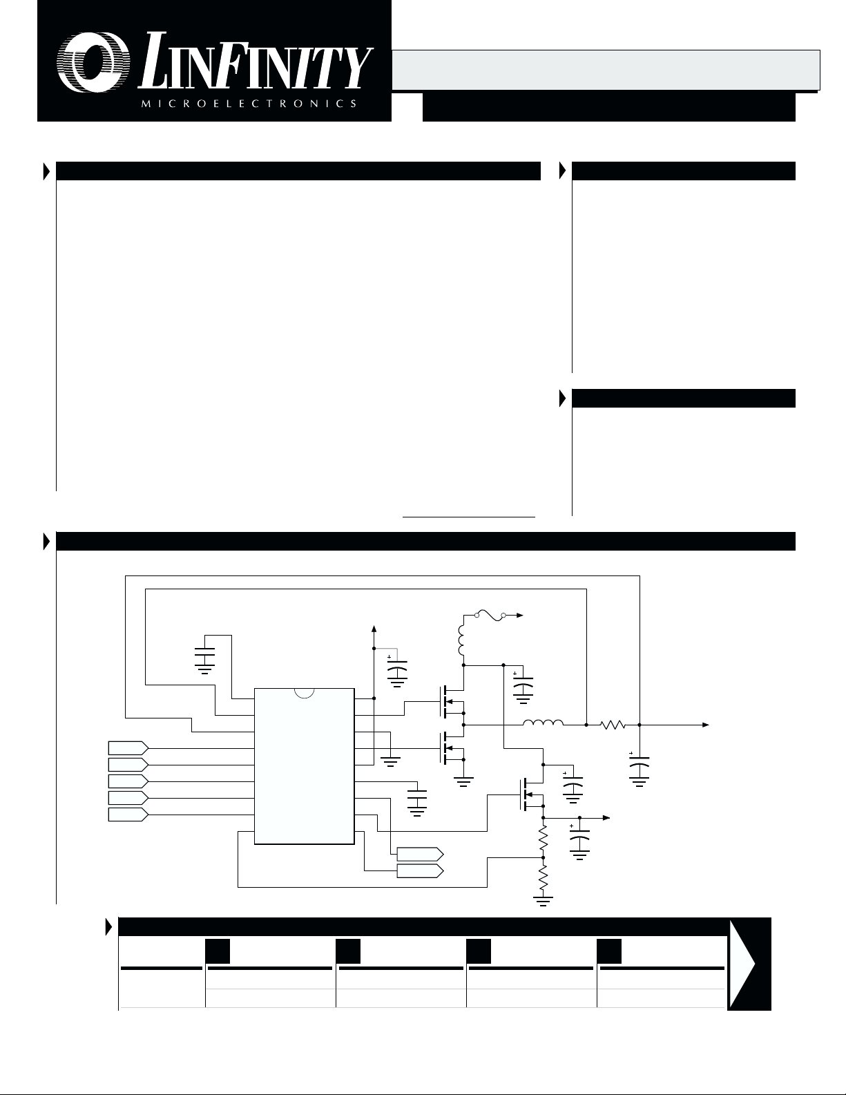
LX1665 IN A PENTIUM II SINGLE-CHIP POWER SUPPLY SOLUTION
L
1µH
C
8
680pF
F1 20A
2
Q
IRL3102
Q
IRL3303
D
1
2
Q
4
IRLZ44
Plastic SOIC
16-pin
5V
6.3V
1500µF x3
C
2
L
1
2.5µH
R
5
R
6
R
1
0.0025
C
9
330µF
Supply Voltage
for CPU Core
C
1
6.3V, 1500µF x 3**
** Three capacitors for Pentium
Four capacitors for Pentium II
Supply Voltage
For I/O Chipset or GTL+ Bus
C
7
330µF
Plastic SOIC Wide
DW
18-pin
12V
C
3
VID0
VID1
VID2
VID3
VID4
0.1µF
U1
LX1665
1
SS
2
INV
3
V
CC_CORE
4
VID0
5
VID1
6
VID2
7
VID3 OV
8
VID4 L
9
L
FB
Wide-Body SOIC
PWRGD
18-pin
V
TDRV
GND
BDRV
V
DRV
18
C1
17
16
15
14
CC
13
C
T
12
11
10
C
5
1µF
OV
PWRGD
PACKAGE ORDER INFORMATION
T
(°C)
A
Plastic DIP
N
16-pin
Plastic DIP
N
18-pin
0 to 70 LX1664CN LX1665CN LX1664CD LX1665CDW
LX1664ACN LX1665ACN LX1664ACD LX1665ACDW
Note: All surface-mount packages are available in Tape & Reel. Append the letter "T" to part number. (e.g. LX1664CDT)
V
OUT
for
See next page
Selection Guide
Copyright © 1999
Rev. 1.2 11/99
L INF INITY MICROELECTRONICS INC.
11861 WESTERN AVENUE, GARDEN GROVE, CA. 92841, 714-898-8121, FAX: 714-893-2570
1
Page 2
PRODUCT DATABOOK 1996/1997
LX1664/64A, LX1665/65A
DUAL OUTPUT PWM CONTROLLERS WITH 5-BIT DAC
P RODUCTION DATA SHEET
DESCRIPTION (con't.)
Smallest Package Size. The LX1664 is
available in a narrow body 16-pin surface
mount IC package for space sensitive applications. The LX1665 provides the additional
functions of Over Voltage Protection (OVP)
and Power Good (PWRGD) output drives
for applications requiring output voltage
monitoring and protection functions.
Ultra-Fast Transient Response re-
duces system cost. The modulated off-
time architecture results in the fastest tran-
sient response for a given inductor, reducing output capacitor requirements, and reducing the total regulator system cost.
Over-Voltage Protection and Power
Good Flag. The OVP output in the LX1665
& LX1665A can be used to drive an SCR
crowbar circuit to protect the load in the
event of a short-circuit of the main MOSFET.
The LX1665 & LX1665A also have a logiclevel Power Good Flag to signal when the
output voltage is out of specified limits.
DEVICE SELECTION GUIDE
OVP and Current-Sense
DEVICE Packages Power Good Comp. Thresh. (mV) Optimal Load
LX1664 16-pin SOIC
LX1664A & DIP 60 Pentium II (> 10A)
LX1665 18-pin SOIC
LX1665A & DIP 60 Pentium II (> 10A)
No
Yes
100 Pentium-class (<10A)
100 Pentium-class (<10A)
ABSOLUTE MAXIMUM RATINGS (Note 1)
Supply Voltage (VC1) .................................................................................................... 25V
Supply Voltage (VCC) .................................................................................................... 15V
Output Drive Peak Current Source (500ns)............................................................... 1.5A
Output Drive Peak Current Sink (500ns) ................................................................... 1.5A
Input Voltage (SS, INV, V
Operating Junction Temperature
, CT, VID0-VID4) ........................................... -0.3V to 6V
CC_CORE
Plastic (N, D & DW Packages) ............................................................................. 150°C
Storage Temperature Range .................................................................... -65°C to +150°C
Lead Temperature (Soldering, 10 Seconds) ............................................................. 300°C
Note 1. Exceeding these ratings could cause damage to the device. All voltages are with respect
to Ground. Currents are positive into, negative out of the specified terminal. Pin
numbers refer to DIL packages only.
THERMAL DATA
N (16-PIN DIP) PACKAGE:
THERMAL RESISTANCE-JUNCTION TO AMBIENT,
N (18-PIN DIP) PACKAGE:
THERMAL RESISTANCE-JUNCTION TO AMBIENT,
D PACKAGE:
THERMAL RESISTANCE-JUNCTION TO AMBIENT,
DW PACKAGE:
THERMAL RESISTANCE-JUNCTION TO AMBIENT,
Junction Temperature Calculation: TJ = TA + (PD x θJA).
The θJA numbers are guidelines for the thermal performance of the device/pc-board system.
All of the above assume no ambient airflow
θθ
θ
θθ
JA
θθ
θ
θθ
JA
θθ
θ
θθ
JA
θθ
θ
θθ
JA
65°C/W
60°C/W
120°C/W
90°C/W
PACKAGE PIN OUTS
1 16
SS
215
INV
314
V
CC_CORE
413
VID0
512
VID1
611
VID2
710
VID3
89
VID4
N PACKAGE — 16-Pin
LX1664/1664A (Top View)
1 18
SS
217
INV
316
V
CC_CORE
415
VID0
514
VID1
613
VID2
712
VID3
811
VID4
910
L
FB
N PACKAGE — 18-Pin
LX1665/1665A (Top View)
1 16
SS
215
INV
V
CC_CORE
VID0
VID1
VID2
VID3
VID4
314
413
512
611
710
89
D PACKAGE — 16-Pin
LX1664/1664A (Top View)
1 18
SS
217
INV
L
FB
316
415
514
613
712
811
910
V
CC_CORE
VID0
VID1
VID2
VID3
VID4
DW PACKAGE — 18-Pin
LX1665/1665A (Top View)
V
C1
TDRV
GND
BDRV
V
CC
C
T
L
DRV
L
FB
V
C1
TDRV
GND
BDRV
V
CC
C
T
OV
L
DRV
PWRGD
V
C1
TDRV
GND
BDRV
V
CC
C
T
L
DRV
L
FB
V
TDRV
GND
BDRV
V
C
OV
L
DRV
PWRGD
C1
CC
T
2
Copyright © 1999
Rev. 1.2 11/99
Page 3
PRODUCT DATABOOK 1996/1997
LX1664/1664A, LX1665/65A
DUAL OUTPUT PWM CONTROLLERS WITH 5-BIT DAC
P RODUCTION DATA SHEET
ELECTRICAL CHARACTERISTICS
(
Unless otherwise specified, 10.8 < VCC < 13.2, 0°C ≤ TA ≤ 70°C. Test conditions: VCC = 12V, T = 25°C. Use Application Circuit.
Parameter
Symbol
Test Conditions
Reference & DAC Section (See Table 1 - Next Page)
Regulation Accuracy (See Table 1) (Less 40mV output adaptive positioning), VCC = 12V, I
Regulation Accuracy 1.8V ≤ V
OUT
≤ 2.8V
Timing Section
Off Time Initial OT V
Off Time Temp Stability V
Discharging Current I
Ramp Peak V
Ramp Peak-Valley V
DISVCC_CORE
P
RPPVCC_CORE
Ramp Valley Delay to Output 10% Overdrive
= 1.3V, CT = 390pF
CC_CORE
V
= 3.5V, CT = 390pF
CC_CORE
= 1.3V to 3.5V
CC_CORE
= 1.3V, VCT = 1.5V
= 1.3V
V
= 3.5V
CC_CORE
Error Comparator Section
Input Bias Current I
Input Offset Voltage V
EC Delay to Output 10% Overdrive
B
IO
1.3V < VSS = V
< 3.5V
INV
Current Sense Section
Input Bias Current (V
Pulse By Pulse C
L
CS Delay to Output 10% Overdrive
Pin) I
CC_CORE
LX1664/1665 V
1.3V < V
B
Initial Accuracy
CLP
INV
LX1664A/1665A Initial Accuracy
= V
CC_CORE
< 3.5V
Output Drivers Section
Drive Rise Time TRVC1 = VCC = 12V, CL = 3000pF
Drive Fall Time TFVC1 = VCC = 12V, CL = 3000pF
Drive High V
Drive Low V
Output Pull Down V
DHVCC
VCC = VCC = 12V, I
DLVCC
VCC = VCC = 12V, I
PDVCC
= VCC = 12V, I
= VCC = 12V, I
= VC = 0, I
PULL UP
= 20mA
SOURCE
= 200mA
SINK
= 20mA
SOURCE
= 200mA
SINK
= 2mA
UVLO and S.S. Section
Start-Up Threshold V
Hysteresis V
SS Sink Current I
SS Sat Voltage V
ST
HYST
SD
OLVC1
VC1 = 10.1V
= 9V, ISD = 200µA
Supply Current Section
Dynamic Operating Current I
VCC = VC1 = 12V, Out Freq = 200kHz, CL = 0
CD
Power Good / Over-Voltage Protection Section (LX1665 Only)
Lower Threshold (V
Hysteresis
Power Good Voltage Low I
Over-Voltage Threshold (V
OVP Sourcing Current VOV = 5V
CC_CORE
PWRGD
CC_CORE
/ DAC
= 5mA
/ V
DAC
)
OUT
)
Linear Regulator Section
Output Voltage Set by external resistors
Setpoint Accuracy IL = 0.5A using 0.5% resistors
Output Temperature Drift
Load Regulation
Cummulative Accuracy
Op-Amp Output Current Open Loop
LOAD
= 6A
LX1664/1665 (A)
Min. Typ. Max.
-30 30 mV
-1 1 %
180 210 240 µA
0.9 1 1.1 V
0.37 0.42 0.47 V
36 41 46 mV
85 100 115 mV
50 60 70 mV
9.9 10.1 10.4 V
2 5.5 mA
88 90 92 %
110 117 125 %
30 45 mA
1.5 3.6 V
-1.5 1.5 %
50 70 mA
)
Units
2µs
1µs
40 ppm
2V
100 ns
0.8 2 µA
200 ns
27 35 µA
200 ns
70 ns
70 ns
11 V
10 V
0.06 0.1 V
0.8 1.2 V
0.8 1.4 V
0.31 V
0.15 0.6 V
27 mA
1%
0.5 0.7 V
40 ppm
1.5 %
3%
Copyright © 1999
Rev. 1.2 11/99
3
Page 4
PRODUCT DATABOOK 1996/1997
0A
5A/Div.
Time - 100µs/Div.
2.8V
100mV/Div.
Output Load
0 to 14A
Output Voltage
LX1664/64A, LX1665/65A
DUAL OUTPUT PWM CONTROLLERS WITH 5-BIT DAC
P RODUCTION DATA SHEET
ELECTRICAL CHARACTERISTICS
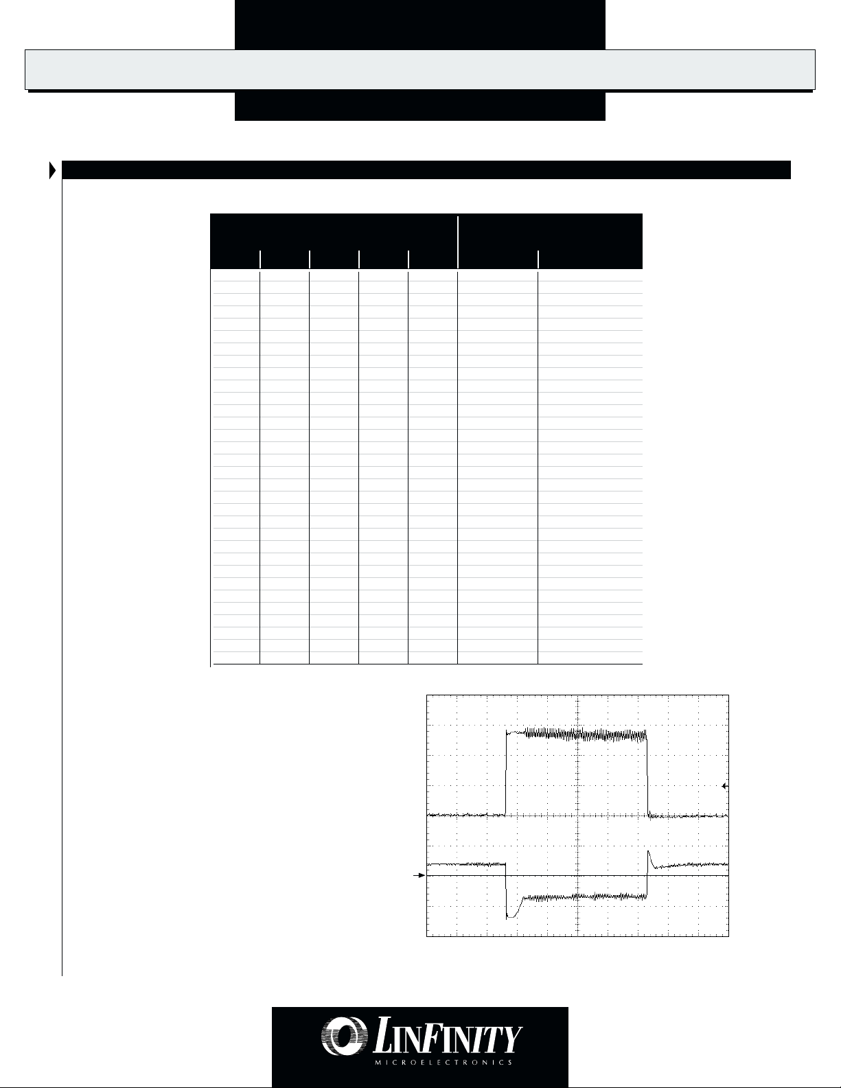
Table 1 - Adaptive Transient Voltage Output (Output Voltage Setpoint Typical)
Processor Pins
0 = Ground, 1 = Open (Floating)
VID4 VID3 VID2 VID1 VID0
01111 1.34V 1.30V
01110 1.39V 1.35V
01101 1.44V 1.40V
01100 1.49V 1.45V
01011 1.54V 1.50V
01010 1.59V 1.55V
01001 1.64V 1.60V
01000 1.69V 1.65V
00111 1.74V 1.70V
00110 1.79V 1.75V
00101 1.84V 1.80V
00100 1.89V 1.85V
00011 1.94V 1.90V
00010 1.99V 1.95V
00001 2.04V 2.00V
00000 2.09V 2.05V
11111 2.04V 2.00V
11110 2.14V 2.10V
11101 2.24V 2.20V
11100 2.34V 2.30V
11011 2.44V 2.40V
11010 2.54V 2.50V
11001 2.64V 2.60V
11000 2.74V 2.70V
10111 2.84V 2.80V
10110 2.94V 2.90V
10101 3.04V 3.00V
10100 3.14V 3.10V
10011 3.24V 3.20V
10010 3.34V 3.30V
10001 3.44V 3.40V
10000 3.54V 3.50V
* Nominal = DAC setpoint voltage with no adaptive output voltage positioning.
Output Voltage (V
0.0A Nominal Output*
CC_CORE
)
Note:
Adaptive Transient Voltage Output
In order to improve transient response a 40mV
offset is built into the Current Sense comparator.
At high currents, the peak output voltage will be
lower than the nominal set point, as shown in
Figure 1. The actual output voltage will be a
function of the sense resistor, the output current
and output ripple.
4
FIGURE 1 — Output Transient Response
(using 5mΩ sense resistor and 5µH output inductor)
Copyright © 1999
Rev. 1.2 11/99
Page 5
PRODUCT DATABOOK 1996/1997
LX1664/1664A, LX1665/65A
DUAL OUTPUT PWM CONTROLLERS WITH 5-BIT DAC
P RODUCTION DATA SHEET
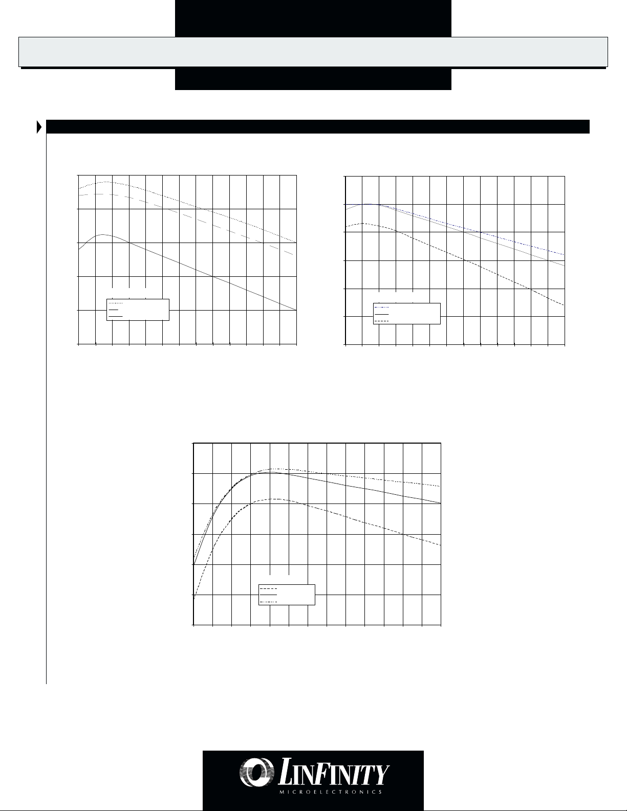
CHARACTERISTICS CURVES
95
90
85
EFFICIENCY (%)__
80
Output Set Point
EFFICIENCY AT 3.1V
75
70
1234567891011121314
EFFICIENCY AT 2.8V
EFFICIENCY AT 1.8V
I
OUT
(A)
FIGURE 2 — Efficiency Test Results:
Non-Synchronous Operation, VIN = 5V
90
100
95
90
85
EFFICIENCY (%)__
80
75
70
Output Set Point
EFFICIENCY AT 3.1V
EFFICIENCY AT 2.8V
EFFICIENCY AT 1.8V
1234567891011121314
I
(A)
OUT
FIGURE 3 — Efficiency Test Results:
Synchronous Operation, VIN = 5V
85
80
75
70
Output Se t Point
1.8V EFF ICIENCY
65
60
1234567891011121314
FIGURE 4 — Efficiency Test Results: Synchronous Operation, V
2.8V EFF ICIENCY
3.3V EFF ICIENCY
I
(A)
OUT
= 12V.
IN
Note: Non-synchronous operation not recommended for 12V operation, due to power loss in Schottky diode.
Copyright © 1999
Rev. 1.2 11/99
5
Page 6
PRODUCT DATABOOK 1996/1997
LX1664/64A, LX1665/65A
DUAL OUTPUT PWM CONTROLLERS WITH 5-BIT DAC
P RODUCTION DATA SHEET
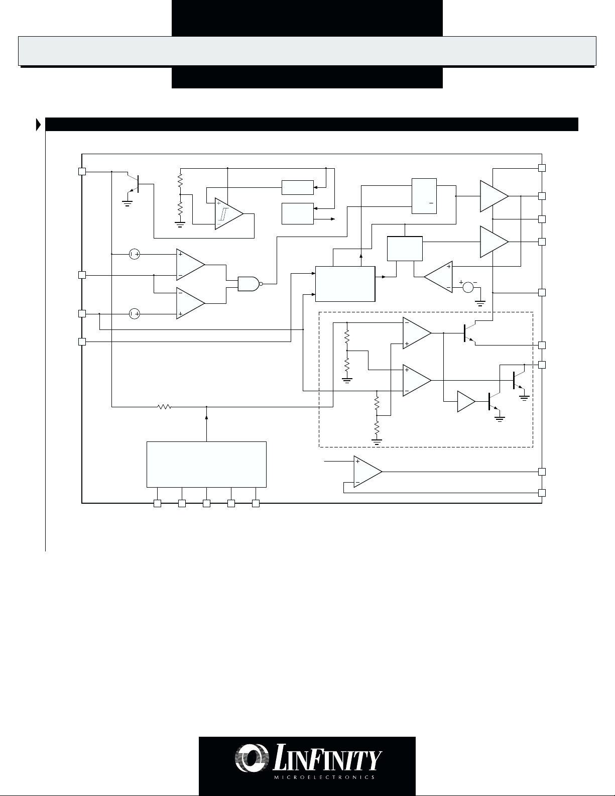
BLOCK DIAGRAM
V
CC
2V Out
UVLO
10.6/10.1
Error Comp
CS Comp
V
INV
CC_CORE
1
SS
40mV
2
100mV
3
**
Trimmed
2V REF
Internal
V
CC
V
REG
Off-Time
Controller
R DOM
Break
Before
Make
PWM Latch
S
RQ
SYNC EN
Comp
OV Comp
V
18
C1
Q
0.7V
TDRV
17
GND
16
BDRV
15
V
14
CC
13
C
T
UV Comp
10k
DAC OUT
LX1665/1665A ONLY
DAC
4 5
VID0 VID16VID27VID38VID4
1.5V
Linear Op Amp
Note: Pin numbers are correct for LX1665/1665A, 18-pin package.
* Not connected on LX1664/1664A.
** 60mV in LX1664A/1665A.
12
10
11
9
OV*
PWRGD*
L
DRV
L
FB
FIGURE 5 — LX1664/1665 Block Diagram
6
Copyright © 1999
Rev. 1.2 11/99
Page 7

PRODUCT DATABOOK 1996/1997
DUAL OUTPUT PWM CONTROLLERS WITH 5-BIT DAC
P RODUCTION DATA SHEET
FUNCTIONAL PIN DESCRIPTION
Pin LX1664 LX1665
Name Pin # Pin # Description
LX1664/1664A, LX1665/65A
SS 1 1
INV 2 2
V
CC_CORE
33
VID0 4 4
VID1 5 5
VID2 6 6
VID3 7 7
VID4 8 8
L
FB
99
PWRGD N.C. 10
L
DRV
10 11
OV N.C. 12
C
T
V
CC
11 13
12 14
BDRV 13 15
GND 14 16
TDRV 15 17
V
C1
16 18
Soft-Start pin, internally connected to the non-inverting input of the error comparator.
Inverting input of the error comparator.
Output voltage. Connected to non-inverting input of the current-sense comparator.
Voltage Identification pin (LSB) input used to set output voltage.
Voltage Identification pin (2nd SB) input.
Voltage Identification pin (3rd SB) input.
Voltage Identification pin (4th SB) input.
Voltage Identification pin (MSB) input. This pin is also the range select pin — when low
(CLOSED), output voltage is set to between 1.30 and 2.05V in 0.05V increments. When high
(OPEN), output is adjusted from 2.0 to 3.5V in 0.1V increments.
Linear regulator feedback pin. 1.5V reference is connected to a resistor divider to set desired
output voltage.
Open collector output pulls low when the output voltage is out of limits.
Linear regulator drive pin. Connect to gate of MOSFET for linear regulator function.
SCR driver goes high when the processor's supply is over specified voltage limits.
The off-time is programmed by connecting a timing capacitor to this pin.
This is the (12V) supply to the IC, as well as gate drive to the bottom FET.
This is the gate drive to the bottom FET. Leave open in non-synchronous operation (when bottom
FET is replaced by a Schottky diode).
Both power and signal ground of the device.
Gate drive for top MOSFET.
This pin is a separate power supply input for the top drive. Can be connected to a charge pump
when only 12V is available.
Copyright © 1999
Rev. 1.2 11/99
7
Page 8

PRODUCT DATABOOK 1996/1997
LX1664/64A, LX1665/65A
DUAL OUTPUT PWM CONTROLLERS WITH 5-BIT DAC
P RODUCTION DATA SHEET
THEORY OF OPERATION
IC OPERATION
Referring to the block diagram and typical application circuit, the
output turns ON the top MOSFET, allowing the inductor current to
increase. At the error comparator threshold, the PWM latch is reset,
the top MOSFET turns OFF and the synchronous MOSFET turns ON.
The OFF-time capacitor C
valley voltage, the synchronous MOSFET turns OFF and the top
is now allowed to discharge. At the
T
MOSFET turns on. A special break-before-make circuit prevents
simultaneous conduction of the two MOSFETS.
The V
response. The INV pin is connected to the positive side of the
pin is offset by +40mV to enhance transient
CC_CORE
current sense resistor, so the controller regulates the positive side
of the sense resistor. At light loads, the output voltage will be
regulated above the nominal setpoint voltage. At heavy loads, the
output voltage will drop below the nominal setpoint voltage. To
minimize frequency variation with varying output voltage, the OFFtime is modulated as a function of the voltage at the V
CC_CORE
pin.
ERROR VOLTAGE COMPARATOR
The error voltage comparator compares the voltage at the positive
side of the sense resistor to the set voltage plus 40mV. An external
filter is recommended for high-frequency noise.
CURRENT LIMIT
Current limiting is done by sensing the inductor current. Exceeding
the current sense threshold turns the output drive OFF and latches
it OFF until the PWM latch Set input goes high again. See Current
Limit Section in "Using The LX1664/65 Devices" later in this data
sheet.
OFF-TIME CONTROL TIMING
The timing capacitor C
timing capacitor is quickly charged during the ON time of the top
allows programming of the OFF-time. The
T
MOSFET and allowed to discharge when the top MOSFET is OFF.
In order to minimize frequency variations while providing different
supply voltages, the discharge current is modulated by the voltage
at the V
V
CC_CORE
pin. The OFF-time is inversely proportional to the
CC_CORE
voltage.
UNDER VOLTAGE LOCKOUT
The purpose of the UVLO is to keep the output drive off until the
input voltage reaches the start-up threshold. At voltages below the
start-up voltage, the UVLO comparator disables the internal biasing,
and turns off the output drives. The SS (Soft-Start) pin is pulled low.
SYNCHRONOUS CONTROL
The synchronous control section incorporates a unique breakbefore-make function to ensure that the primary switch and the
synchronous switch are not turned on at the same time. Approximately 100 nanoseconds of deadtime is provided by the breakbefore-make circuitry to protect the MOSFET switches.
PROGRAMMING THE OUTPUT VOLTAGE
The output voltage is set by means of a 5-bit digital Voltage
Identification (VID) word (See Table 1). The VID code may be hardwired into the package of the processor which do not have a VID
code, the output voltage can be set by means of a DIP switch or
jumpers. For a low or '0' signal, connect the VID pin to ground (DIP
switch ON); for a high or '1' signal, leave the VID pin open (DIP
switch OFF).
The five VID pins on the LX166x series are designed to interface
directly with a Pentium Pro or Pentium II processor. Therefore, all
inputs are expected to be either ground or floating. Any floating
input will be pulled high by internal connections. If using a Socket
7 processor, or other load, the VID code can be set directly by
connecting jumpers or DIP switches to the VID[0:4] pins.
The VID pins are not designed to take TTL inputs, and
should not be connected high. Unpredictable output voltages
may result. If the LX166x devices are to be connected to a logic
circuit, such as BIOS, for programming of output voltage, they
should be buffered using a CMOS gate with open-drain, such as a
74HC125 or 74C906.
POWER GOOD SIGNAL (LX1665 only)
An open collector output is provided which presents high impedance when the output voltage is between 90% and 117% of the
programmed VID voltage, measured at the SS pin. Outside this
window the output presents a low impedance path to ground. The
Power Good function also toggles low during OVP operation.
OVER-VOLTAGE PROTECTION
The controller is inherently protected from an over-voltage condition due to its constant OFF-time architecture. However, should a
failure occur at the power switch, an over-voltage drive pin is
provided (on the LX1665 only) which can drive an external SCR
crowbar (Q
removed and power recycled for the LX1665 to resume normal
), and so blow a fuse (F1). the fault condition must be
3
operation (See Figure 9).
LINEAR REGULATOR
The product highlight application shows an application schematic
using a MOSFET as the pass element for a linear regulator. this
output is suitable for converting the 5V system supply to 3.3V for
processor I/O buffers, memory, chipset and other components. The
output can be adjusted to any voltage between 1.5V and 3.6V in
order to supply other (lower) power requirements on a motherboard. See section "Using the LX1664/1665 Devices" at the end of
this data sheet.
8
Copyright © 1999
Rev. 1.2 11/99
Page 9

PRODUCT DATABOOK 1996/1997
SS
TDRV
V
CC
INV
V
CC_CORE
VID0
VID1
VID2
VID3 L
DRV
C
T
BDRV
GND
V
C1
U1
LX1664
VID3
C
5
1µF
12V
R
1
V
OUT
5V
16-pin
Narrow Body SOIC
Q
1
IRL3102
L1, 2.5µH
6.3V, 1500µF x 3**
14
13
12
11
10
9
1
2
3
4
5
6
7
C
8
680pF
VID2
VID1
VID0
VID4
C
3
0.1µF
2.5m9
Supply Voltage
for CPU Core
6.3V
1500µF x3
** Three capacitors for Pentium
Four capacitors for Pentium II
VID4 L
FB
Supply Voltage
For I/O Chipset or GTL+ Bus
8
16
15
Q
2
IRL3303
C
2
C
1
Q
4
IRLZ44
R
5
R
6
C
7
330µF
C
9
330µF
SS
TDRV
V
CC
INV
V
CC_CORE
VID0
VID1
VID2
VID3 L
DRV
C
T
BDRV
GND
V
C1
U1
LX1664
VID3
C
5
1µF
12V
R
1
V
OUT
5V
16-pin
Narrow Body SOIC
Q
1
IRL3102
L
1
, 5µH
6.3V, 1500µF x 3**
14
13
12
11
10
9
1
2
3
4
5
6
7
C
8
680pF
VID2
VID1
VID0
VID4
C
3
0.1µF
0.005
Supply Voltage
for CPU Core
6.3V
1500µF x3
** Three capacitors for Pentium
Four capacitors for Pentium II
VID4 L
FB
D
1
Supply Voltage
For I/O Chipset or GTL+ Bus
8
16
15
C
2
C
1
Q
4
IRLZ44
R
5
R
6
C
7
330µF
C
9
330µF
LX1664/1664A, LX1665/65A
DUAL OUTPUT PWM CONTROLLERS WITH 5-BIT DAC
P RODUCTION DATA SHEET
APPLICATION INFORMATION
Copyright © 1999
Rev. 1.2 11/99
FIGURE 6 — LX1664 In A Pentium / Socket 7 Single-Chip Power Supply Controller Solution (Synchronous)
FIGURE 7 — LX1664 In A Non-Synchronous / Socket 7 Power Supply Application
9
Page 10

PRODUCT DATABOOK 1996/1997
LX1664/64A, LX1665/65A
DUAL OUTPUT PWM CONTROLLERS WITH 5-BIT DAC
P RODUCTION DATA SHEET
APPLICATION INFORMATION
C
3
VID0
VID1
VID2
VID3
VID4
0.1µF
1
2
3
4
5
6
7
8
9
U1
LX1665
SS
INV
V
CC_CORE
VID0
VID1
VID2
VID3 OV
VID4 L
L
FB
18-pin
Wide Body SOIC
V
TDRV
GND
BDRV
V
PWRGD
18
C1
17
16
15
14
CC
13
C
T
12
11
DRV
10
12V
C
5
1µF
OV
PWRGD
L
1µH
C
8
680pF
2
F1 15A
Q
1
IRL3102
Q
2
IRL3303
C
2
6.3V
1500µF x3
Q
4
IRLZ44
R
5V
5
C
S
R
S
L
1
2.5µH
5V or 3.3V
Supply
C
9
330µF
C
7
330µF
Supply Voltage
for CPU Core
V
C
1
6.3V, 1500µF x 3
** Three capacitors for Pentium
Four capacitors for Pentium II
1.5V for
GTL+ Bus Supply
OUT
VID0
VID1
VID2
VID3
VID4
R
6
FIGURE 8 — VRM 8.2 (Pentium II / Deschutes) Reference Design With Loss-Less Current Sensing
12V
20A
1
5V
6.3V
1500µF x3
C
2
1
2
L
1
2.5µH
C
9
330µF
R
1
0.0025
Supply Voltage
for CPU Core
Q3
SCR
2N6504
Q
4
R
IRLZ44
5
Supply Voltage
For I/O Chipset or GTL+ Bus
C
7
330µF
C
0.1µF
D
2
1N4148 1N4148
3
U1
LX1665
1
SS
2
INV
3
V
CC_CORE
4
VID0
5
VID1
6
VID2
7
VID3 OV
8
VID4 L
9
L
FB
PWRGD
V
TDRV
GND
BDRV
V
DRV
18
C1
17
16
15
14
CC
13
C
T
12
11
10
C
1µF
R2, 10k
5
C
8
1500µF
C10
0.1µF
R
7
10
D
3
D
4
1N5817
F
Q
IRL3303
Q
IRL3102
18-pin
Wide-Body SOIC
PWRGD
V
OUT
C
1
6.3V, 1500µF x 3**
Four capacitors for Pentium II
** Three capacitors for Pentium
10
R
6
FIGURE 9 — Full-Featured Pentium II Processor Supply With 12V Power Input
Copyright © 1999
Rev. 1.2 11/99
Page 11

PRODUCT DATABOOK 1996/1997
LX1664/1664A, LX1665/65A
DUAL OUTPUT PWM CONTROLLERS WITH 5-BIT DAC
P RODUCTION DATA SHEET
BILL OF MATERIALS
LX1665 Bill of Materials (Refer to Product Highlight)
Ref Description Part Number / Manufacturer Qty.
C
1
C
2
C7, C
9
C
3
C
4
C
8
C
5
L
1
L
2
Q
1
Q
2
Q
3
R5, R
6
R
1
U1 Controller IC LX1665CDW Linfinity 1
Total 21
1500µF, 6.3V capacitor MV-GX Sanyo 4
1500µF, 6.3V capacitor MV-GX Sanyo 2
330µF, Electrolytic MV-GX Sanyo 2
0.1µF SMD Cap 1
390pF SMD Cap 1
680pF SMD Cap 1
1µF, 16V SMD Ceramic 1
2.5µH Inductor HM0096832 BI or equivalent 1
1µH Inductor 1
MOSFET IRL3102 International Rectifier or equivalent 1
MOSFET IRL3303 International Rectifier or equivalent 1
MOSFET IRLZ44 International Rectifier or equivalent 1
Resistor (See Table 6 for values) SMD Resistor 2
2.5mΩ Sense Resistor IRC OARS-1 or PCB trace 1
USING THE LX1664/65 DEVICES
The LX1664/65 devices are very easy to design with, requiring
only a few simple calculations to implement a given design. The
following procedures and considerations should provide effective operation for virtually all applications. Refer to the Appli-
cation Information section for component reference designators.
TIMING CAPACITOR SELECTION
The frequency of operation of the LX166x is a function of duty
cycle and OFF-time. The OFF-time is proportional to the timing
capacitor (which is shown as C
this data sheet), and is modulated to minimize frequency
in all application schematics in
8
variations with duty cycle. The frequency is constant, during
steady-state operation, due to the modulation of the OFF-time.
The timing capacitor (CT) should be selected using the
following equation:
C
(1 - V
=
T
fS (1.52 - 0.29 * V
Where I
(recommended to be around 200kHz for optimal operation and
is fixed at 200µA and fS is the switching frequency
DIS
OUT /VIN
) * I
DIS
OUT
)
component selection).
When using a 5V input voltage, the switching frequency (f
can be approximated as follows:
I
CT = 0.621
DIS
*
f
S
Choosing a 680pF capacitor will result in an operating
frequency of 183kHz at V
is used, he capacitor value must be changed (the optimal timing
= 2.8V. When a 12V power input
OUT
capacitor for 12V input will be in the range of 1000-1500pF).
L
OUTPUT INDUCTOR SELECTION
1
The inductance value chosen determines the ripple current
present at the output of the power supply. Size the inductance
to allow a nominal ±10% swing above and below the nominal DC
load current, using the equation L = V
OFF-time, VL is the voltage across the inductor during the OFFtime, and ∆I is peak-to-peak ripple current in the inductor. Be
sure to select a high-frequency core material which can handle
the DC current, such as 3C8, which is sized for the correct power
level. Typical inductance values can range from 2 to 10µH.
Note that ripple current will increase with a smaller inductor.
Exceeding the ripple current rating of the capacitors could cause
reliability problems.
* ∆T/∆I, where ∆T is the
L
)
S
Copyright © 1999
Rev. 1.2 11/99
11
Page 12

PRODUCT DATABOOK 1996/1997
LX1664/64A, LX1665/65A
DUAL OUTPUT PWM CONTROLLERS WITH 5-BIT DAC
P RODUCTION DATA SHEET
USING THE LX1664/65 DEVICES
INPUT INDUCTOR SELECTION
In order to cope with faster transient load changes, a smaller
output inductor is needed. However, reducing the size of the
output inductor will result in a higher ripple voltage on the input
supply. This noise on the 5V rail can affect other loads, such as
graphics cards. It is recommended that a smaller input inductor,
L
(1 - 1.5µH), is used on the 5V rail to filter out the ripple. Ensure
2
that this inductor has the same current rating as the output
inductor.
FILTER CAPACITOR SELECTION
C
1
The capacitors on the output of the PWM section are used to filter
the output current ripple, as well as help during transient load
conditions, and the capacitor bank should be sized to meet ripple
and transient performance specifications.
When a transient (step) load current change occurs, the output
voltage will have a step which equals the product of the Effective
Series Resistance (ESR) of the capacitor and the current step (∆I).
when current increases from low (in sleep mode) to high, the
output voltage will drop below its steady state value. In the
advanced microprocessor power supply, the capacitor should
usually be selected on the basis of its ESR value, rather than the
capacitance or RMS current capability. Capacitors that satisfy the
ESR requirement usually have a larger capacitance and current
capability than needed for the application. The allowable ESR can
be found by:
C1 FILTER CAPACITOR SELECTION (continued)
aluminum electrolytic, and have demonstrated reliability. The
Oscon series from Sanyo generally provides the very best
performance in terms of long term ESR stability and general
reliability, but at a substantial cost penalty. The MV-GX series
provides excellent ESR performance, meeting all Intel transient
specifications, at a reasonable cost. Beware of off-brand, very-low
cost filter capacitors, which have been shown to degrade in both
ESR and general electrolyte characteristics over time.
CURRENT LIMIT
Current limiting occurs when a sensed voltage, proportional to
load current, exceeds the current-sense comparator threshold
value. The current can be sensed either by using a fixed sense
resistor in series with the inductor to cause a voltage drop
proportional to current, or by using a resistor and capacitor in
parallel with the inductor to sense the voltage drop across the
parasitic resistance of the inductor.
The LX166x family offers two different comparator thresholds.
The LX1664 & 1665 have a threshold of 100mV, while the LX1664A
and LX1665A have a threshold of 60mV. The 60mV threshold is
better suited to higher current loads, such as a Pentium II or
Deschutes processor.
Sense Resistor
The current sense resistor, R1, is selected according to the formula:
ESR * (I
RIPPLE
+ ∆I) < V
EX
Where VEX is the allowable output voltage excursion in the
transient and I
as the LX166x series, have adaptive output voltage positioning,
is the inductor ripple current. Regulators such
RIPPLE
which adds 40mV to the DC set-point voltage — VEX is therefore
the difference between the low load voltage and the minimum
dynamic voltage allowed for the microprocessor.
Ripple current is a function of the output inductor value (L
and can be approximated as follows:
V
I
RIPPLE
- V
IN
fS * L
OUT
OUT
=
V
OUT
*
V
IN
OUT
Where fS is the switching frequency.
Electrolytic capacitors can be used for the output filter capacitor bank, but are less stable with age than tantalum capacitors. As
they age, their ESR degrades, reducing the system performance
and increasing the risk of failure. It is recommended that multiple
parallel capacitors are used so that, as ESR increases with age,
overall performance will still meet the processor's requirements.
There is frequently strong pressure to use the least expensive
components possible, however, this could lead to degraded longterm reliability, especially in the case of filter capacitors. Linfinity's
demo boards use Sanyo MV-GX filter capacitors, which are
R1 = V
Where V
for LX1664/65 and 60mV for LX1664A/65A) and I
current limit. Typical choices are shown below.
/ I
TRIP
TRIP
is the current sense comparator threshold (100mV
TRIP
TRIP
TABLE 2 - Current Sense Resistor Selection Guide
Sense Resistor Recommended
Load Value Controller
),
Pentium-Class Processor (<10A) 5mΩ LX1664 or LX1665
Pentium II Class (>10A) 2.5mΩ LX1664A or LX1665A
A smaller sense resistor will result in lower heat dissipation (I²R)
and also a smaller output voltage droop at higher currents.
There are several alternative types of sense resistor. The
surface-mount metal “staple” form of resistor has the advantage of
exposure to free air to dissipate heat and its value can be
controlled very tightly. Its main drawback, however, is cost. An
alternative is to construct the sense resistor using a copper PCB
trace. Although the resistance cannot be controlled as tightly, the
PCB trace is very low cost.
is the desired
12
Copyright © 1999
Rev. 1.2 11/99
Page 13

PRODUCT DATABOOK 1996/1997
LX1664/1664A, LX1665/65A
DUAL OUTPUT PWM CONTROLLERS WITH 5-BIT DAC
P RODUCTION DATA SHEET
USING THE LX1664/65 DEVICES
CURRENT LIMIT (continued)
PCB Sense Resistor
A PCB sense resistor should be constructed as shown in Figure
10. By attaching directly to the large pads for the capacitor and
inductor, heat is dissipated efficiently by the larger copper masses.
Connect the current sense lines as shown to avoid any errors.
Inductor
2.5m9
100mil Wide, 850mil Long
2.5mm x 22mm (2 oz/ft
Sense Resistor
2
copper)
Output
Capacitor Pad
Sense Lines
FIGURE 10 — Sense Resistor Construction Diagram
Recommended sense resistor sizes are given in the following
table:
TABLE 3 - PCB Sense Resistor Selection Guide
Copper Copper Desired Resistor Dimensions (w x l)
Weight Thickness Value mm inches
2
2 oz/ft
68µm 2.5m
5m
Ω
Ω
2.5 x 22 0.1 x 0.85
2.5 x 43 0.1 x 1.7
Loss-Less Current Sensing Using Resistance of Inductor
Any inductor has a parasitic resistance, RL, which causes a DC
voltage drop when current flows through the inductor. Figure 11
shows a sensor circuit comprising of a surface mount resistor, RS,
and capacitor, CS, in parallel with the inductor, eliminating the
current sense resistor.
L
R
L
Load
R
S
Current
Sense
C
S
R
S2
V
CS
Comparator
FIGURE 11 — Current Sense Circuit
CURRENT LIMIT
(continued)
The current flowing through the inductor is a triangle wave. If the
sensor components are selected such that:
L/R
= RS * C
L
S
The voltage across the capacitor will be equal to the current
flowing through the resistor, i.e.
VCS = ILR
L
Since VCS reflects the inductor current, by selecting the
appropriate RS and CS, VCS can be made to reach the comparator
voltage (60mV for LX166xA or 100mV for the LX166x) at the
desired trip current.
Design Example
(Pentium II circuit, with a maximum static current of 14.2A)
The gain of the sensor can be characterized as:
M
|T(
j
)|
R
L
L/RSC
S
M
1/R
SCSRL
/L
FIGURE 12 — Sensor Gain
The dc/static tripping current I
V
I
trip,S
trip
=
R
L
satisfies:
trip,S
Select L/RSCS ≤ RL to have higher dynamic tripping current
than the static one. The dynamic tripping current I
V
=
trip
L/(RSCS)
I
trip,d
General Guidelines for Selecting RS , CS, and R
V
trip
RL = Select: RS ≤ 10 kΩ
I
trip,S
and CS according to: CSn =
L
RL R
n
S
L
satisfies:
trip,d
The above equation has taken into account the current-dependency of the inductance.
The test circuit (Figure 6) used the following parameters:
RL = 3mΩ, RS = 9kΩ, CS = 0.1µF, and L is 2.5µH at 0A current.
Copyright © 1999
Rev. 1.2 11/99
13
Page 14

PRODUCT DATABOOK 1996/1997
LX1664/64A, LX1665/65A
DUAL OUTPUT PWM CONTROLLERS WITH 5-BIT DAC
P RODUCTION DATA SHEET
USING THE LX1664/65 DEVICES
CURRENT LIMIT (continued)
In cases where RL is so large that the trip point current would
be lower than the desired short-circuit current limit, a resistor (R
can be put in parallel with C
of components is as follows:
R
L (Required)
R
L (Actual)
C
= =
S
R
L (Actual)
=
* (RS2 // RS)
, as shown in Figure 11. The selection
S
R
S2
RS2 + R
S
L
R
L (Actual)
L
*
RS + R
RS2 * R
S2
S2
S
Again, select (RS2//RS) < 10kΩ.
FET SELECTION
To insure reliable operation, the operating junction temperature
of the FET switches must be kept below certain limits. The Intel
specification states that 115°C maximum junction temperature
should be maintained with an ambient of 50°C. This is achieved
by properly derating the part, and by adequate heat sinking. One
of the most critical parameters for FET selection is the R
resistance. This parameter directly contributes to the power
DS
ON
dissipation of the FET devices, and thus impacts heat sink design,
mechanical layout, and reliability. In general, the larger the
current handling capability of the FET, the lower the RDS ON will
be, since more die area is available.
TABLE 4 - FET Selection Guide
This table gives selection of suitable FETs from International Rectifier.
Device R
IRL3803 6 83 30
IRL22203N 7 71 30
IRL3103 14 40 30
IRL3102 13 56 20
IRL3303 26 24 30
IRL2703 40 17 30
All devices in TO-220 package. For surface mount devices (TO-263 /
D2-Pak), add 'S' to part number, e.g. IRL3103S.
@ ID @ Max. Break-
DS(ON)
ΩΩ
10V (m
Ω)T
ΩΩ
= 100°C down Voltage
C
The recommended solution is to use IRL3102 for the high side
and IRL3303 for the low side FET, for the best combination of cost
and performance. Alternative FET’s from any manufacturer could
be used, provided they meet the same criteria for R
DS(ON)
.
Heat Dissipated In Upper MOSFET
The heat dissipated in the top MOSFET will be:
P
= (I2 * R
D
* Duty Cycle) + (0.51 * VIN * tSW * fS )
DS(ON)
FET SELECTION (continued)
For the IRL3102 (13mΩ R
)
will result in typical heat dissipation of 1.48W.
), converting 5V to 2.8V at 14A
DS(ON)
Synchronous Rectification – Lower MOSFET
The lower pass element can be either a MOSFET or a Schottky
diode. The use of a MOSFET (synchronous rectification) will result
in higher efficiency, but at higher cost than using a Schottky diode
(non-synchronous).
Power dissipated in the bottom MOSFET will be:
P
= I2 * R
D
[IRL3303 or 1.12W for the IRL3102]
* [1 - Duty Cycle] = 2.24W
DS(ON)
Catch Diode – Lower MOSFET
A low-power Schottky diode, such as a 1N5817, is recommended
to be connected between the gate and source of the lower
MOSFET when operating from a 12V-power supply (see Figure 9).
This will help protect the controller IC against latch-up due to the
inductor voltage going negative. Although latch-up is unlikely, the
use of such a catch diode will improve reliability and is highly
recommended.
Non-Synchronous Operation - Schottky Diode
A typical Schottky diode, with a forward drop of 0.6V will dissipate
0.6 * 14 * [1 – 2.8/5] = 3.7W (compared to the 1.1 to 2.2W dissipated
by a MOSFET under the same conditions). This power loss
becomes much more significant at lower duty cycles – synchronous rectification is recommended especially when a 12V-power
input is used. The use of a dual Schottky diode in a single TO-220
package (e.g. the MBR2535) helps improve thermal dissipation.
MOSFET GATE BIAS
The power MOSFETs can be biased by one of two methods:
charge pump or 12V supply connected to VC1.
1) Charge Pump (Bootstrap)
When 12V is supplied to the drain of the MOSFET, as in
Figure 9, the gate drive needs to be higher than 12V in order
to turn the MOSFET on. Capacitor C10 and diodes D2 & D
are used as a charge pump voltage doubling circuit to raise
the voltage of VC1 so that the TDRV pin always provides a
high enough voltage to turn on Q1. The 12V supply must
always be connected to VCC to provide power for the IC
itself, as well as gate drive for the bottom MOSFET.
2) 12V Supply
When 5V is supplied to the drain of Q1, a 12V supply should
be connected to both VCC and VC1.
3
Where t
and fS is the switching frequency.
is switching transition line for body diode (~100ns)
SW
14
Copyright © 1999
Rev. 1.2 11/99
Page 15

PRODUCT DATABOOK 1996/1997
LX1664/1664A, LX1665/65A
DUAL OUTPUT PWM CONTROLLERS WITH 5-BIT DAC
P RODUCTION DATA SHEET
USING THE LX1664/65 DEVICES
LINEAR REGULATOR
Referring to the front page Product Highlight, a schematic is
presented which uses a MOSFET as a series pass element for a
linear regulator. The MOSFET is driven by the LX1664 controller,
and down-converts a +5V or +3.3V supply to the desired V
level, between 1.5 & 3.5V, as determined by the feedback
OUT
resistors.
The current available from the Linear regulator is dictated by
the supply capability, as well as the MOSFET ratings, and will
typically lie in the 3-5 ampere range. This output is well suited
for I/O buffers, memory, chipset and other components. Using
3.3V supply to convert to 1.5V for GTL+ Bus will significantly
reduce heat dissipation in the MOSFET.
MOSFET Comments
Heatsinking the MOSFET becomes important, since the linear
stage output current could approach 5 amperes in some applications. Since there are no switching losses, power dissipation in
the MOSFET is simply defined by P
current. This means that a +5V
the MOSFET dissipate (5-3.3) * 5 = 8.5 watts. This amount of
IN
D
to +3.3V
= (VIN - V
at 5A will require that
OUT
) * I output
OUT
power in a MOSFET calls for a heatsink, which will be the same
physical size as that required for a monolithic LDO, such as the
LX8384 device.
The dropout voltage for the linear regulator stage is the product
of R
ON * I
DS
voltage will be (worst case) 37 milliohms x 5A = 185mV.
Note that the R
affect heat dissipation, only dropout voltage. For reasons of
. Using a 2SK1388 device at 5A, the dropout
OUT
ON of the (linear regulator) MOSFET does not
DS
economy, a FET with a higher resistance can be chosen for the
linear regulator, e.g. 2SK1388 or IRLZ44.
TABLE 5 - Linear Regulator MOSFET Selection Guide
Device R
IRFZ24N 70 12 55
IRL2703 40 17 30
IRLZ44N 22 29 55
@ ID @ Max. Break-
DS(ON)
ΩΩ
10V (m
Ω)T
ΩΩ
= 100°C down Voltage
C
Avoiding Crosstalk
To avoid a load transient on the switching output affecting the
linear regulator, follow these guidelines:
1) Separate 5V supply traces to switching & linear FETs as
much as possible.
2) Place capacitor C9 as close to drain of Q4 as possible.
Typical transient response is shown in Figure 13.
LINEAR REGULATOR
(continued)
FIGURE 13 — Typical Transient Response
Channel 2 = Linear Regulator Output.
Set point = 3.3V @ 2A (20mV/div.)
Channel 4 = Switching Regulator Output.
set point = 2.8V
V
Channel 3 = Switching Regulator Load Current
CC_CORE
Transient 0 - 13A
Output Voltage Setting
As shown in Application Information Figures 6-9, two resistors (R
& R6) set the linear regulator stage output voltage:
V
= 1.5 * (R5 + R6) / R
OUT
6
As an example, to set resistor magnitudes, assume a desired
V
of 3.3 volts:
OUT
1.5 * (12.1k + 10k) / 10k = 3.3 volts (approximately)
In general, the divider resistor values should be in the vicinity
of 10-12k ohm for optimal noise performance. Please refer to
Table 6.
5
Copyright © 1999
Rev. 1.2 11/99
15
Page 16

PRODUCT DATABOOK 1996/1997
t
LX1664/64A, LX1665/65A
DUAL OUTPUT PWM CONTROLLERS WITH 5-BIT DAC
P RODUCTION DATA SHEET
USING THE LX1664/65 DEVICES
LINEAR REGULATOR (continued)
TABLE 6 -
Resistors Settings for Linear Regulator Output Voltage
Nominal
Set Point (V) R
3.3 12 10 3.30
3.2 11.3 10 3.20
3.1 11.3 10.7 3.08
3.0 11 11 3.00
2.9 10.3 11 2.90
2.8 10 11.5 2.80
2.7 10 12.4 2.71
2.6 10 13.7 2.59
2.5 9.76 14.7 2.50
2.4 8.87 14.7 2.41
2.3 8.87 16.5 2.31
2.2 8.87 18.7 2.21
2.1 8.87 22.1 2.10
2.0 8.87 26.7 2.00
1.9 8.87 21 2.13
1.8 7.15 35.7 1.80
1.7 7.15 53.6 1.70
1.6 7.15 100 1.61
1.5 7.15 ∞ 1.50
ΩΩ
(k
Ω)R6 (k
ΩΩ
5
ΩΩ
Ω)V
ΩΩ
OUT
(V)
Capacitor Selection
Referring to the Product Highlight schematic on the front page, the
standard value to use as the linear regulator stage output capacitor
is on the order of 330µF. This provides sufficient hold-up for all
expected transient load events in memory and I/O circuitry.
Disabling Linear Output
Linear regulator output can be disabled by pulling feedback pin
(L
) up to 5V as shown in Figure 14.
FB
TABLE 7 - Linear Enable (LIN EN) Function Table
LIN EN LIN OUTPUT
H Disabled
L Enabled
5V
LIN EN
LX1664
L
DRV
L
FB
10k
10
9
10k
2N2222
C
0.1µF
10
R
R
5
6
Q
4
IRLZ44
C
9
330µF
C
330µF
Supply Voltage
For I/O Chipse
7
LAYOUT GUIDELINES - THERMAL DESIGN
A great deal of time and effort were spent optimizing the thermal
design of the demo boards. Any user who intends to implement
an embedded motherboard would be well advised to carefully
read and follow these guidelines. If the FET switches have been
carefully selected, external heatsinking is generally not required.
However, this means that copper trace on the PC board must now
be used. This is a potential trouble spot;
as much copper area as
possible must be dedicated to heatsinking the FET switches, and
the diode as well if a non-synchronous solution is used.
In our VRM module, heatsink area was taken from internal
ground and VCC planes which were actually split and connected
with VIAS to the power device tabs. The TO-220 and TO-263
cases are well suited for this application, and are the preferred
packages. Remember to remove any conformal coating from all
exposed PC traces which are involved in heatsinking.
General Notes
As always, be sure to provide local capacitive decoupling close to
the chip. Be sure use ground plane construction for all highfrequency work. Use low ESR capacitors where justified, but be
alert for damping and ringing problems. High-frequency designs
demand careful routing and layout, and may require several
iterations to achieve desired performance levels.
Power Traces
To reduce power losses due to ohmic resistance, careful consideration should be given to the layout of traces that carry high
currents. The main paths to consider are:
■ Input power from 5V supply to drain of top MOSFET.
■ Trace between top MOSFET and lower MOSFET or Schottky
diode.
■ Trace between lower MOSFET or Schottky diode and
ground.
■ Trace between source of top MOSFET and inductor, sense
resistor and load.
Input
5V or 12V
LX166x
Output
16
FIGURE 14 — Enabling Linear Regulator
FIGURE 15 — Power Traces
Copyright © 1999
Rev. 1.2 11/99
Page 17

PRODUCT DATABOOK 1996/1997
DUAL OUTPUT PWM CONTROLLERS WITH 5-BIT DAC
P RODUCTION DATA SHEET
USING THE LX1664/65 DEVICES
LAYOUT GUIDELINES - THERMAL DESIGN (continued)
All of these traces should be made as wide and thick as
possible, in order to minimize resistance and hence power losses.
It is also recommended that, whenever possible, the ground, input
and output power signals should be on separate planes (PCB
layers). See Figure 15 – bold traces are power traces.
C5 Input Decoupling (VCC) Capacitor
Ensure that this 1µF capacitor is placed as close to the IC as
possible to minimize the effects of noise on the device.
RELATED DEVICES
LX1662/1663 - Single Output PWM Controllers
LX1553 - PWM Controller for 5V - 3.3V Conversion
LX1668 - Triple Output PWM Controller
LX1664/1664A, LX1665/65A
Layout Assistance
Please contact Linfinity’s Applications Engineers for assistance
with any layout or component selection issues. A Gerber file
with layout for the most popular devices is available upon request.
Evaluation boards are also available upon request. Please
check Linfinity's web site for further application notes.
Copyright © 1999
Rev. 1.2 11/99
Cyrix is a registered trademark and 6x86 and Gx86 are trademarks of Cyrix Corporation. K6 is a trademark of AMD.
Power PC is a trademark of International Business Machines Corporation. Alpha is a trademark of Digital Equipment Corporation.
PRODUCTION DATA - Information contained in this document is proprietary to LinFinity, and is current as of publication date. This document
may not be modified in any way without the express written consent of LinFinity. Product processing does not necessarily include testing of
all parameters. Linfinity reserves the right to change the configuration and performance of the product and to discontinue product at any time.
Pentium is a registered trademark of Intel Corporation.
17
 Loading...