

Datasheet LX1554CPW, LX1554CM, LX1554CDM, LX1553IM, LX1553IDM Datasheet (Microsemi Corporation)
...Page 1
Copyright © 1994
Rev. 1.0a 1/01
FOR FURTHER INFORMATION CALL (714) 898-8121
11861 WESTERN AVENUE , GARDEN GROVE, CA. 92841
1
U
LTRA-LOW START-UP CURRENT
, C
URRENT-MODE
PWM
PRODUCTION DATA SHEET
THE INFINITE POWER OF INNOVATION
LX1552/3/4/5
LIN DOC #:
1552
DESCRIPTION KEY FEATURES
■■
■■
■ULTRA-LOW START-UP CURRENT
(150µA typ.)
■■
■■
■TRIMMED OSCILLATOR DISCHARGE
CURRENT (±2% typ.)
■■
■■
■INITIAL OSCILLATOR FREQUENCY BETTER
THAN ±4%
■■
■■
■OUTPUT PULLDOWN DURING UVLO
■■
■■
■PRECISION 2.5V REFERENCE (±2% max.)
pCURRENT SENSE DELAY TO OUTPUT
(150ns typ.)
pAUTOMATIC FEED FORWARD
COMPENSATION
pPULSE-BY-PULSE CURRENT LIMITING
pENHANCED LOAD RESPONSE
CHARACTERISTICS
pUNDER-VOLTAGE LOCKOUT WITH
HYSTERESIS
pDOUBLE PULSE SUPPRESSION
pHIGH CURRENT TOTEM POLE OUTPUT
(±1Amp peak)
p500kHz OPERATION
The LX155X family of ultra-low start-up
current (250µA max.), current mode
control IC's offer new levels of energy
efficiency for offline converter applications. They are ideally optimized for
personal computer and CRT power
supplies although they can be used in
any number of off-line applications
where energy efficiency is critical.
Coupled with the fact that the LX155X
series requires a minimal set of external
components, the series offers an
excellent value for cost conscious
consumer applications.
Optimizing energy efficiency, the
LX155X series demonstrates a significant power reduction as compared with
other similar off-line controllers. Table 1
compares the SG384X, UC384XA and
the LX155X start-up resistor power
dissipation. The LX155X offers an
overall 4X reduction in power dissipa-
tion. Additionally, the precise oscillator
discharge current gives the power
supply designer considerable flexibility
in optimizing system duty cycle
consistency.
The current mode architecture
demonstrates improved load regulation,
pulse by pulse current limiting and
inherent protection of the power supply
output switch. The LX155X includes a
bandgap reference trimmed to 1%, an
error amplifier, a current sense comparator internally clamped to 1V, a high
current totem pole output stage for fast
switching of power mosfet's, and an
externally programmable oscillator to
set operating frequency and maximum
duty cycle. The undervoltage lock-out
circuitry is designed to operate with as
little as 250µA of supply current
permitting very efficient bootstrap
designs.
PRODUCT HIGHLIGHT
PACKAGE ORDER INFORMATION
T
A
(°C)
Plastic DIP
8-pin
0 to 70 LX155xCM LX155xCDM LX155xCD — LX155xCPW
-40 to 85 LX155xIM LX155xIDM LX155xID — —
-55 to 125 — — — LX155xMY —
M
Plastic SOIC
8-pin
DM
Plastic SOIC
14-pin
D
Ceramic DIP
8-pin
Y
TSSOP
20-pin
PW
TYPICAL APPLICATION OF LX155X USING ITS
MICROPOWER START-UP FEATURE
Max. Start-up Current
Specification (I
ST
)
Typical Start-Up
Resistor Value (R
ST
)
Max. Start-Up Resistor
Power Dissipation (PR)
Design Using
SG384xUC384xALX155x
1000µA
500µA 250µA
2.26W1.13W0.56W
62K
ΩΩ
ΩΩ
Ω 124K
ΩΩ
ΩΩ
Ω248K
ΩΩ
ΩΩ
Ω
Note:Calculation is done for universal AC input specification of V
ACMIN
= 90V
RMS
to V
ACMAX
= 265V
RMS
using the
following equation: (Resistor current is selected to be
2 * I
ST
at V
ACMIN
.)
RST =, P
R
=
V
AC MIN
√2 * I
ST
2V
AC2 MAX
R
ST
TABLE 1
APPLICATIONS
■■
■■
■ECONOMY OFF-LINE FLYBACK OR
FORWARD CONVERTERS
■DC-DC BUCK OR BOOST CONVERTERS
■LOW COST DC MOTOR CONTROL
AVAILABLE OPTIONS PER PART #
Part # Start-UpHysteresisMax.Duty
Voltage Cycle
LX1552 16V 6V <100%
LX1553 8.4V 0.8V <100%
LX1554 16V 6V <50%
LX1555 8.4V 0.8V <50%
I
ST
R
ST
V
CC
AC
INPUT
LX1552
or
LX1554
Note: All surface-mount packages are available in Tape & Reel. Append the letter "T" to part number. (i.e. LX1552CDMT)
Page 2
U
LTRA-LOW START-UP CURRENT
, C
URRENT-MODE
PWM
LX1552/3/4/5
PRODUCT DATABOOK 1996/1997
Copyright © 1994
Rev. 1.0a 1/01
2
P
RODUCTION DATA SHEET
ABSOLUTE MAXIMUM RATINGS (Note 1)
Supply Voltage (Low Impedance Source)..................................................................30V
Supply Voltage (I
CC
< 30mA).........................................................................Self Limiting
Output Current.............................................................................................................±1A
Output Energy (Capacitive Load)................................................................................5µJ
Analog Inputs (Pins 2, 3)...........................................................................-0.3V to +6.3V
Error Amp Output Sink Current...............................................................................10mA
Power Dissipation at TA = 25°C (DIL-8)......................................................................1W
Operating Junction Temperature
Ceramic (Y Package)............................................................................................150°C
Plastic (M, DM, D, PW Packages)........................................................................150°C
Storage Temperature Range....................................................................-65°C to +150°C
Lead Temperature (Soldering, 10 Seconds)............................................................300°C
PACKAGE PIN OUTS
V
REF
V
CC
OUTPUT
GND
COMP
V
FB
I
SENSE
RT/C
T
1 8
27
36
45
M & Y PACKAGE
(Top View)
DM PACKAGE
(Top View)
V
REF
V
CC
OUTPUT
GND
COMP
V
FB
I
SENSE
RT/C
T
1 8
27
36
45
V
REF
N.C.
V
CC
V
C
OUTPUT
GND
PWR GND
COMP
N.C.
V
FB
N.C.
I
SENSE
N.C.
RT/C
T
1 14
213
312
411
510
69
78
D PACKAGE
(Top View)
PW PACKAGE
(Top View)
1 20
219
318
417
516
615
714
813
912
10 11
N.C.
N.C.
COMP
V
FB
N.C.
I
SENSE
N.C.
RT/C
T
N.C.
N.C.
N.C.
N.C.
V
REF
N.C.
V
CC
V
C
OUTPUT
GND
PWR GND
N.C.
M PACKAGE:
THERMAL RESISTANCE-JUNCTION TO AMBIENT,
θθ
θθ
θ
JA
95°C/W
DM PACKAGE:
THERMAL RESISTANCE-JUNCTION TO AMBIENT,
θθ
θθ
θ
JA
165°C/W
D PACKAGE:
THERMAL RESISTANCE-JUNCTION TO AMBIENT,
θθ
θθ
θ
JA
120°C/W
Y PACKAGE:
THERMAL RESISTANCE-JUNCTION TO AMBIENT,
θθ
θθ
θ
JA
130°C/W
PW PACKAGE:
THERMAL RESISTANCE-JUNCTION TO AMBIENT,
θθ
θθ
θ
JA
144°C/W
Junction Temperature Calculation: T
J
= TA + (PD x θJA).
The θ
JA
numbers are guidelines for the thermal performance of the device/pc-board system.
All of the above assume no ambient airflow
THERMAL DATA
Note 1.Exceeding these ratings could cause damage to the device. All voltages are with respect
to Ground. Currents are positive into, negative out of the specified terminal. Pin
numbers refer to DIL packages only.
Page 3
U
LTRA-LOW START-UP CURRENT
, C
URRENT-MODE
PWM
LX1552/3/4/5
PRODUCT DATABOOK 1996/1997
3
Copyright © 1994
Rev. 1.0a 1/01
PRODUCTION DATA SHEET
ELECTRICAL CHARACTERISTICS
(Unless otherwise specified, these specifications apply over the operating ambient temperatures for LX155xC with 0°C ≤ TA ≤ 70°C, LX155xI with -40°C ≤ TA ≤ 85°C, LX155xM
with -55°C ≤ T
A
≤ 125°C; VCC=15V (Note 5); RT=10K; CT=3.3nF. Low duty cycle pulse testing techniques are used which maintains junction and case temperatures equal to the
ambient temperature.)
Reference Section
Parameter
Symbol
Test Conditions
Output Voltage V
REFTA
= 25°C, IL = 1mA
Line Regulation 12 ≤ VIN ≤ 25V
Load Regulation 1 ≤ I
O
≤ 20mA
Temperature Stability (Note 2 & 7)
Total Output Variation Over Line, Load, and Temperature
Output Noise Voltage (Note 2) V
N
10Hz ≤ f ≤ 10kHz, TA = 25°C
Long Term Stability (Note 2) TA = 125°C, t = 1000hrs
Output Short Circuit I
SC
LX155xC
Units
Min.Typ.Max.Min.Typ.Max.
LX155xI/155xM
4.955.005.054.955.005.05 V
620 620mV
625 625mV
0.2 0.4 0.2 0.4 mV/°C
4.9 5.1 4.9 5.1 V
50 50 µV
525 525mV
-30 -100-180 -30 -100-180 mA
Oscillator Section
Initial Accuracy (Note 6) TA = 25°C
TA = 25°C, RT = 698Ω, CT = 22nF, LX1552/3 only
Voltage Stability 12 ≤ V
CC
≤ 25V
Temperature Stability (Note 2) T
MIN
≤ TA ≤ T
MAX
Amplitude (Note 2) V
PIN 4
peak to peak
Discharge Current I
D
TA = 25°C, V
PIN 4
= 2V
V
PIN 4
= 2V, T
MIN
≤ TA ≤ T
MAX
48.550.552.548.550.552.5 kHz
56 58 60 56 58 60 kHz
0.2 1 0.2 1 %
55%
1.7 1.7 V
8.0 8.3 8.6 8.0 8.3 8.6 mA
7.6 8.8 7.8 8.8 mA
Output Voltage Low Level V
OLISINK
= 20mA
I
SINK
= 200mA
Output Voltage High Level V
OHISOURCE
= 20mA
I
SOURCE
= 200mA
Rise Time (Note 2) T
R
TA = 25°C, CL = 1nF
Fall Time (Note 2) TFTA = 25°C, CL = 1nF
UVLO Saturation V
SATVCC
= 5V, I
SINK
= 10mA
Error Amp Section
Current Sense Section
Gain (Note 3 & 4) A
VOL
Maximum Input Signal (Note 3) V
PIN 1
= 5V
Power Supply Rejection Ratio (Note 3) PSRR 12 ≤ VCC ≤ 25V
Input Bias Current I
B
Delay to Output (Note 2) T
PDVPIN 3
= 0 to 2V
Output Section
2.452.502.552.452.502.55 V
-0.1 -1 -0.1 -0.5 µA
65 90 65 90 dB
0.6 0.6 MHz
60 70 60 70 dB
24 24 mA
-0.5 -0.8 -0.5 -0.8 mA
5 6.5 5 6.5 V
0.7 1.1 0.7 1.1 V
2.85 3 3.152.85 3 3.15 V/V
0.9 1 1.1 0.9 1 1.1 V
70 70 dB
-2 -10 -2 -5 µA
150 300 150 300 ns
0.1 0.4 0.1 0.4 V
1.5 2.2 1.5 2.2 V
13 13.5 13 13.5 V
12 13.5 12 13.5 V
50 100 50 100 ns
50 100 50 100 ns
0.7 1.2 0.7 1.2 V
(Electrical Characteristics continue next page.)
Input Voltage V
PIN 1
= 2.5V
Input Bias Current I
B
Open Loop Gain A
VOL
2 ≤ VO ≤ 4V
Unity Gain Bandwidth (Note 2) UGBW TA = 25°C
Power Supply Rejection Ratio (Note 3) PSRR 12 ≤ V
CC
≤ 25V
Output Sink Current I
OLVPIN 2
= 2.7V, V
PIN 1
= 1.1V
Output Source Current I
OHVPIN 2
= 2.3V, V
PIN 1
= 5V
Output Voltage High Level V
OHVPIN 2
= 2.3V, RL = 15K to ground
Output Voltage Low Level V
OLVPIN 2
= 2.7V, RL = 15K to V
REF
Page 4
U
LTRA-LOW START-UP CURRENT
, C
URRENT-MODE
PWM
LX1552/3/4/5
PRODUCT DATABOOK 1996/1997
Copyright © 1994
Rev. 1.0a 1/01
4
P
RODUCTION DATA SHEET
ELECTRICAL CHARACTERISTICS (Con't.)
Under-Voltage Lockout Section
Parameter
Symbol
Test Conditions
Start Threshold VST1552/1554
1553/1555
Min. Operation Voltage After Turn-On 1552/1554
1553/1555
LX155xC
Units
Min.Typ.Max.Min.Typ.Max.
LX155xI/155xM
15 16 17 15 16 17 V
7.8 8.4 9.0 7.8 8.4 9.0 V
9 10 11 9 10 11 V
7.0 7.6 8.2 7.0 7.6 8.2 V
PWM Section
Maximum Duty Cycle 1552/1553
1552/1553, RT = 698Ω, CT = 22nF
1554/1555
Minimum Duty Cycle
94 96 94 96 %
50 50 %
47 48 47 48 %
00%
Power Consumption Section
Start-Up Current I
ST
Operating Supply Current I
CC
VCC Zener Voltage VZICC = 25mA
150 250 150 250 µA
11 17 11 17 mA
30 35 30 35 V
Notes:2.These parameters, although guaranteed, are not 100% tested in
production.
3.Parameter measured at trip point of latch with V
FB
= 0.
4.Gain defined as:A = ; 0 ≤ V
ISENSE
≤ 0.8V.
5.Adjust V
CC
above the start threshold before setting at 15V.
6.Output frequency equals oscillator frequency for the LX1552 and
LX1553. Output frequency is one half oscillator frequency for the
LX1554 and LX1555.
7.Temperature stability, sometimes referred to as average temperature
coefficient, is described by the equation:
Temp Stability =
V
REF
(max.) & V
REF
(min.) are the maximum & minimum reference
voltage measured over the appropriate temperature range. Note that the
extremes in voltage do not necessarily occur at the extremes in
temperature.
V
REF
(max.) - V
REF
(min.)
TA (max.) - TA (min.)
∆ V
COMP
∆ V
ISENSE
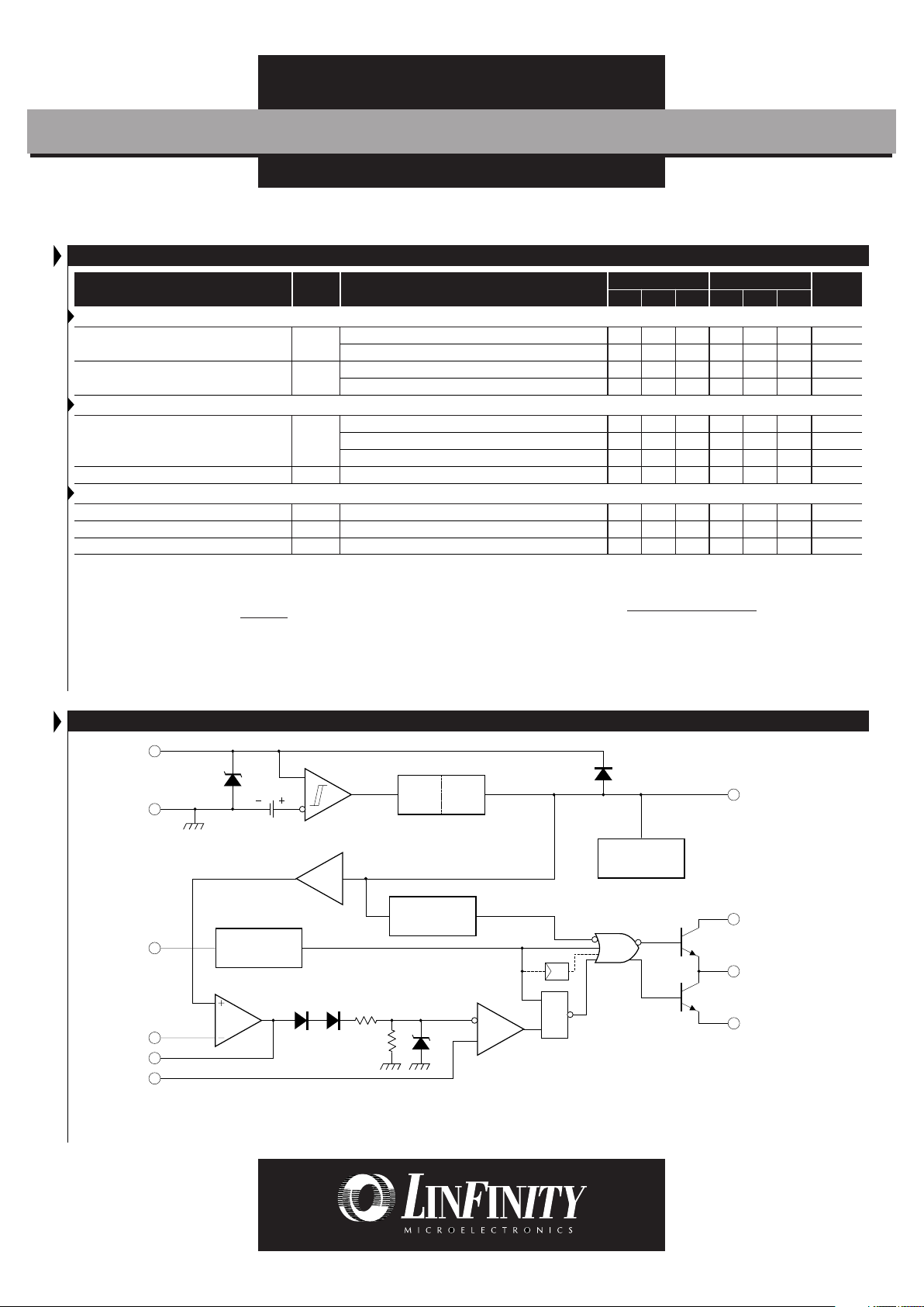
BLOCK DIAGRAM
*
- V
CC
and VC are internally connected for 8 pin packages.
**
- POWER GROUND and GROUND are internally connected for 8 pin packages.
***
- Toggle flip flop used only in 1554 and 1555.
OSCILLATOR
S
R
***
V
REF
GOOD LOGIC
INTERNAL
BIAS
S / R
5V
REF
PWM
LATCH
CURRENT SENSE
COMPARATOR
1V
R
2R
ERROR AMP
16V (1552/1554)
8.4V (1553/1555)
16V (1552/1554)
8.4V (1553/1555)
UVLO
34V
GROUND**
V
CC
*
R
T/CT
V
FB
T
COMP
I
SENSE
POWER GROUND**
OUTPUT
V
C
*
V
REF
Page 5

U
LTRA-LOW START-UP CURRENT
, C
URRENT-MODE
PWM
LX1552/3/4/5
PRODUCT DATABOOK 1996/1997
5
Copyright © 1994
Rev. 1.0a 1/01
PRODUCTION DATA SHEET
GRAPH / CURVE INDEX
Characteristic Curves
FIGURE #
1. OSCILLATOR FREQUENCY vs. TIMING RESISTOR
2. MAXIMUM DUTY CYCLE vs. TIMING RESISTOR
3. OSCILLATOR DISCHARGE CURRENT vs. TEMPERATURE
4. OSCILLATOR FREQUENCY vs. TEMPERATURE
5. OUTPUT INITIAL ACCURACY vs. TEMPERATURE
6. OUTPUT DUTY CYCLE vs. TEMPERATURE
7. REFERENCE VOLTAGE vs. TEMPERATURE
8. REFERENCE SHORT CIRCUIT CURRENT vs. TEMPERATURE
9. E.A. INPUT VOLTAGE vs. TEMPERATURE
10.START-UP CURRENT vs. TEMPERATURE
11.START-UP CURRENT vs. SUPPLY VOLTAGE
12.START-UP CURRENT vs. SUPPLY VOLTAGE
13.DYNAMIC SUPPLY CURRENT vs. OSCILLATOR FREQUENCY
14.CURRENT SENSE DELAY TO OUTPUT vs. TEMPERATURE
15.CURRENT SENSE THRESHOLD vs. ERROR AMPLIFIER OUTPUT
16.START-UP THRESHOLD vs. TEMPERATURE
17.START-UP THRESHOLD vs. TEMPERATURE
18.MINIMUM OPERATING VOLTAGE vs. TEMPERATURE
19.MINIMUM OPERATING VOLTAGE vs. TEMPERATURE
20.LOW LEVEL OUTPUT SATURATION VOLTAGE DURING UNDER-
VOLTAGE LOCKOUT
21.OUTPUT SATURATION VOLTAGE vs. OUTPUT CURRENT and
TEMPERATURE
22.OUTPUT SATURATION VOLTAGE vs. OUTPUT CURRENT and
TEMPERATURE
FIGURE INDEX
Theory of Operation Section
FIGURE #
23.TYPICAL APPLICATION OF START-UP CIRCUITRY
24.REFERENCE VOLTAGE vs. TEMPERATURE
25.SIMPLIFIED SCHEMATIC OF OSCILLATOR SECTION
26.DUTY CYCLE VARIATION vs. DISCHARGE CURRENT
27.OSCILLATOR FREQUENCY vs. TIMING RESISTOR
28.MAXIMUM DUTY CYCLE vs. TIMING RESISTOR
29.CURRENT SENSE THRESHOLD vs. ERROR AMPLIFIER OUTPUT
Typical Applications Section
FIGURE #
30.CURRENT SENSE SPIKE SUPPRESSION
31.MOSFET PARASITIC OSCILLATIONS
32.ADJUSTABLE BUFFERED REDUCTION OF CLAMP LEVEL
WITH SOFT-START
33.EXTERNAL DUTY CYCLE CLAMP AND MULTI-UNIT SYCHRONIZATION
34.SLOPE COMPENSATION
35.OPEN LOOP LABORATORY FIXTURE
36.OFF-LINE FLYBACK REGULATOR
Page 6
U
LTRA-LOW START-UP CURRENT
, C
URRENT-MODE
PWM
LX1552/3/4/5
PRODUCT DATABOOK 1996/1997
Copyright © 1994
Rev. 1.0a 1/01
6
P
RODUCTION DATA SHEET
CHARACTERISTIC CURVES
FIGURE 2. — MAXIMUM DUTY CYCLE vs. TIMING RESISTOR
FIGURE 3. — OSCILLATOR DISCHARGE CURRENT vs.
TEMPERATURE
FIGURE 4. — OSCILLATOR FREQUENCY vs. TEMPERATURE
FIGURE 1. — OSCILLATOR FREQUENCY vs. TIMING RESISTOR
0.1
0
40
(RT) Timing Resistor - (k)
100
Maximum Duty Cycle - (%)
20
50
80
110100
10
60
70
90
30
VCC = 15V
T
A
= 25°C
100
0.1
0.1
1
1000
Oscillator Frequency - (kHz)
(RT) Timing Resistor - (k)
100
10
1
10
VCC = 15V
T
A
= 25°C
CT = 3.3nF
CT = 1nF
CT = 6.8nF
CT = 22nF
CT = 47nF
CT = 0.1µF
7.70
8.10
(TA) Ambient Temperature - (°C)
(I
d
) Oscillator Discharge Current - (mA)
7.90
8.20
7.80
8.30
8.40
8.00
-75
-50 -25 0 25 50 75 100 125
8.50
VCC = 15V
V
PIN4
= 2V
45
49
(TA) Ambient Temperature - (°C)
Oscillator Frequency - (KHz)
47
50
46
51
52
48
-75
-50 -25 0 25 50 75 100 125
53
VCC = 15V
R
T
= 10k
C
T
= 3.3nF
54
55
Page 7

U
LTRA-LOW START-UP CURRENT
, C
URRENT-MODE
PWM
LX1552/3/4/5
PRODUCT DATABOOK 1996/1997
7
Copyright © 1994
Rev. 1.0a 1/01
PRODUCTION DATA SHEET
CHARACTERISTIC CURVES
FIGURE 6. — OUTPUT DUTY CYCLE vs. TEMPERATURE
FIGURE 7. — REFERENCE VOLTAGE vs. TEMPERATURE FIGURE 8. — REFERENCE SHORT CIRCUIT CURRENT vs.
TEMPERATURE
FIGURE 5. — OUTPUT INITIAL ACCURACY vs. TEMPERATURE
40
44
(TA) Ambient Temperature - (°C)
Output Duty Cycle - (%)
42
45
41
46
47
43
-75
-50 -25 0 25 50 75 100 125
48
VCC = 15V
R
T
= 698
W
C
T
= 22nF
50.0
56.0
(TA) Ambient Temperature - (°C)
Output Initial Accuracy - (kHz)
53.0
57.5
51.5
59.0
60.5
54.5
-75
-50 -25 0 25 50 75 100 125
62.0
VCC = 15V
R
T
= 698
W
C
T
= 22nF
63.5
65.0
LX1552 and LX1553 only
4.95
4.99
(TA) Ambient Temperature - (°C)
(V
REF
) Reference Voltage - (V)
4.97
5.00
4.96
5.01
5.02
4.98
-75
-50 -25 0 25 50 75 100 125
5.03
VCC = 15V
I
L
= 1mA
30
90
(TA) Ambient Temperature - (°C)
(I
SC
) Reference Short Circuit Current - (mA)
60
105
45
120
135
75
-75
-50 -25 0 25 50 75 100 125
180
150
165
Page 8

U
LTRA-LOW START-UP CURRENT
, C
URRENT-MODE
PWM
LX1552/3/4/5
PRODUCT DATABOOK 1996/1997
Copyright © 1994
Rev. 1.0a 1/01
8
P
RODUCTION DATA SHEET
CHARACTERISTIC CURVES
FIGURE 10. — START-UP CURRENT vs. TEMPERATURE
FIGURE 11. — START-UP CURRENT vs. SUPPLY VOLTAGE FIGURE 12. — START-UP CURRENT vs. SUPPLY VOLTAGE
FIGURE 9. — E.A. INPUT VOLTAGE vs. TEMPERATURE
0
100
(TA) Ambient Temperature - (°C)
(I
ST
) Start-Up Current - (µA)
50
125
25
150
175
75
-75
-50 -25 0 25 50 75 100 125
250
200
225
LX1552/LX1554
LX1553/LX1555
2.45
2.49
(TA) Ambient Temperature - (°C)
E.A. Input Voltage - (V)
2.47
2.50
2.46
2.51
2.52
2.48
-75
-50 -25 0 25 50 75 100 125
2.55
2.53
2.54
VCC = 15V
0
100
(VCC) Supply Voltage - (V)
(I
ST
) Start-Up Current - (µA)
50
125
25
150
175
75
0
2 4 6 8 10 12 14 20
250
200
225
16 18
LX1553/LX1555
T
A
= 25°C
0
100
(VCC) Supply Voltage - (V)
(I
ST
) Start-Up Current - (µA)
50
125
25
150
175
75
0
1234567 10
250
200
225
89
LX1552/LX1554
T
A
= 25°C
Page 9

U
LTRA-LOW START-UP CURRENT
, C
URRENT-MODE
PWM
LX1552/3/4/5
PRODUCT DATABOOK 1996/1997
9
Copyright © 1994
Rev. 1.0a 1/01
PRODUCTION DATA SHEET
CHARACTERISTIC CURVES
FIGURE 14. — CURRENT SENSE DELAY TO OUTPUT vs.
TEMPERATURE
FIGURE 15. — CURRENT SENSE THRESHOLD vs.
ERROR AMPLIFIER OUTPUT
FIGURE 16. — START-UP THRESHOLD vs. TEMPERATURE
FIGURE 13. — DYNAMIC SUPPLY CURRENT vs.
OSCILLATOR FREQUENCY
0
120
(TA) Ambient Temperature - (°C)
(T
pd
) C.S. Delay to Output - (ns)
60
150
30
180
210
90
-75
-50 -25 0 25 50 75 100 125
300
240
270
VCC = 15V
V
PIN3
= 0V to 2V
C
L
= 1nF
100
10
0
12
Oscillator Frequency - (kHz)
30
(I
CC
) Dynamic Supply Current - (mA)
6
15
24
1000
3
18
21
27
9
TA = 25°C
R
T
= 10k
C
L
= 1000pF
VIN = 16V
V
IN
= 12V
V
IN
= 10V
7.8
8.2
(TA) Ambient Temperature - (°C)
Start-Up Trheshold - (V)
8.0
8.3
7.9
8.4
8.5
8.1
-75
-50 -25 0 25 50 75 100 125
8.6
LX1553
LX1555
8.7
8.8
0
0.4
Error Amplifier Output Voltage - (V)
Current Sense Threshold - (V)
0.2
0.5
0.1
0.6
0.7
0.3
0
0.5 1.0 1.5 2.0 2.5 3.0 3.5 5.0
1.0
0.8
0.9
4.0 4.5
TA = 25°C
1.1
TA = 125°C
TA = -55°C
Page 10

U
LTRA-LOW START-UP CURRENT
, C
URRENT-MODE
PWM
LX1552/3/4/5
PRODUCT DATABOOK 1996/1997
Copyright © 1994
Rev. 1.0a 1/01
10
P
RODUCTION DATA SHEET
CHARACTERISTIC CURVES
FIGURE 18. — MINIMUM OPERATING VOLTAGE vs.
TEMPERATURE
FIGURE 19. — MINIMUM OPERATING VOLTAGE vs.
TEMPERATURE
FIGURE 20. — LOW LEVEL OUTPUT SATURATION VOLTAGE
DURING UNDER-VOLTAGE LOCKOUT
FIGURE 17. — START-UP THRESHOLD vs. TEMPERATURE
15.0
15.8
(TA) Ambient Temperature - (°C)
Start-Up Trheshold - (V)
15.4
16.0
15.2
16.2
16.4
15.6
-75
-50 -25 0 25 50 75 100 125
16.6
LX1552
LX1554
16.8
17.0
7.0
7.4
(TA) Ambient Temperature - (°C)
Minimum Operating Voltage - (V)
7.2
7.5
7.1
7.6
7.7
7.3
-75
-50 -25 0 25 50 75 100 125
7.8
LX1553
LX1555
7.9
8.0
1
0.1
0.00
0.48
Output Sink Current - (mA)
1.20
(V
SAT
) Output Saturation Voltage - (V)
0.24
0.60
0.96
10
0.12
0.72
0.84
1.08
0.36
VCC = 5V
TA = -55°C
TA = 25°C
TA = 125°C
9.0
9.8
(TA) Ambient Temperature - (°C)
Minimum Operating Voltage - (V)
9.4
10.0
9.2
10.2
10.4
9.6
-75
-50 -25 0 25 50 75 100 125
10.6
LX1552
LX1554
10.8
11.0
Page 11

U
LTRA-LOW START-UP CURRENT
, C
URRENT-MODE
PWM
LX1552/3/4/5
PRODUCT DATABOOK 1996/1997
11
Copyright © 1994
Rev. 1.0a 1/01
PRODUCTION DATA SHEET
CHARACTERISTIC CURVES
FIGURE 21. — OUTPUT SATURATION VOLTAGE vs.
OUTPUT CURRENT and TEMPERATURE
FIGURE 22. — OUTPUT SATURATION VOLTAGE vs.
OUTPUT CURRENT and TEMPERATURE
100
10
0.00
Output Sink Current - (mA)
6.0
(V
SAT
) Output Saturation Voltage - (V)
3.0
100
0
1.0
4.0
2.0
VCC = 5V
Sink Transistor
TA = -55°C
TA = 25°C
TA = 125°C
5.0
100
10
0.00
2.40
Output Source Current - (mA)
6.00
(V
SAT
) Output Saturation Voltage - (V)
1.20
3.00
4.80
1000
0.60
3.60
4.20
5.40
1.80
VCC = 15V
Source Transistor
TA = -55°C
TA = 25°C
TA = 125°C
Page 12

U
LTRA-LOW START-UP CURRENT
, C
URRENT-MODE
PWM
LX1552/3/4/5
PRODUCT DATABOOK 1996/1997
Copyright © 1994
Rev. 1.0a 1/01
12
P
RODUCTION DATA SHEET
THEORY OF OPERATION
IC DESCRIPTION
The LX1552/3/4/5 series of current mode PWM controller IC's are
designed to offer substantial improvements in the areas of startup current and oscillator accuracy when compared to the first
generation products, the UC184x series. While they can be used
in most DC-DC applications, they are optimized for single-ended
designs such as Flyback and Forward converters. The LX1552/
54 series are best suited for off-line applications, whereas the
1553/55 series are mostly used in power supplies with low input
voltages. The IC can be divided into six main sections as shown
in the Block Diagram (page 4): undervoltage lockout and startup circuit; voltage reference; oscillator; current sense comparator
and PWM latch; error amplifier; and the output stage. The
operation of each section is described in the following sections.
The differences between the members of this family are summarized in Table 1.
The start-up capacitor (C1) is charged by current through resistor
(R1) minus the start-up current. Resistor (R1) is designed such
that it provides more than 250µA of current (typically 2x I
ST(max)
).
Once this voltage reaches the start-up threshold, the IC turns on,
starting the switching cycle. This causes an increase in IC
operating current, resulting in discharging the start-up capacitor.
During this time, the auxiliary winding flyback voltage gets
rectified & filtered via (D1) and (C1) and provides sufficient
voltage to continue to operate the IC and support its required
supply current. The start-up capacitor must be large enough such
that during the discharge period, the bootsrap voltage exceeds
the shutdown threshold of the IC.
Table 2 below shows a comparison of start-up resistor power
dissipation vs. maximum start-up current for different devices.
Max. Start-up Current
Specification (IST)
Typical Start-Up
Resistor Value (R
ST
)
Max. Start-Up Resistor
Power Dissipation (PR)
Design Using SG384x UC384xA LX155x
2.26W 1.13W 0.56W
62K
ΩΩ
ΩΩ
Ω 124K
ΩΩ
ΩΩ
Ω 248K
ΩΩ
ΩΩ
Ω
1000µA 500µA 250µA
(Resistor R1 is designed such that it provides 2X maximum
start-up current under low line conditions. Maximum power
dissipation is calculated under maximum line conditions. Example assumes 90 to 265VAC universal input application.)
FIGURE 23 — TYPICAL APPLICATION OF START-UP CIRCUITRY
UNDERVOLTAGE LOCKOUT
The LX155x undervoltage lock-out is designed to maintain an
ultra low quiescent current of less than 250µA, while guaranteeing the IC is fully functional before the output stage is activated.
Comparing this to the SG384x series, a 4x reduction in start-up
current is achieved resulting in 75% less power dissipation in the
start-up resistor. This is especially important in off-line power
supplies which are designed to operate for universal input
voltages of 90 to 265V AC.
Figure 23 shows an efficient supply voltage using the ultra low
start-up current of the LX1554 in conjunction with a bootstrap
winding off of the power transformer. Circuit operation is as
follows.
HysterisesVoltage
(V
HYS
)
PART #
Start-up Voltage
(V
ST
)
LX1552
LX1553
LX1554
LX1555
16V
8.4V
16V
8.4V
6V
0.8V
6V
0.8V
<100%
<100%
<50%
<50%
UVLO
MAXIMUM
DUTY CYCLE
TABLE 1
R
S
GND
DC BUS
C
1
D
1
I1 > 250µA
1ST < 250µA
V
IN
REF
R
T/CT
V
O
GND
R
T
C
T
LX1554
TABLE 2
Page 13

U
LTRA-LOW START-UP CURRENT
, C
URRENT-MODE
PWM
LX1552/3/4/5
PRODUCT DATABOOK 1996/1997
13
Copyright © 1994
Rev. 1.0a 1/01
PRODUCTION DATA SHEET
THEORY OF OPERATION
VOLTAGE REFERENCE
The voltage reference is a low drift bandgap design which
provides +5.0V to supply charging current to the oscillator timing
capacitor, as well as supporting internal circuitries. Initial
accuracy for all devices are specified at ±1% max., which is a 2x
improvement for the commercial product when compared to the
SG384x series. The reference is capable of providing in excess
of 20mA for powering any external control circuitries and has
built-in short circuit protection.
FIGURE 25 — SIMPLIFIED SCHEMATIC OF OSCILLATOR SECTION
OSCILLATOR
The oscillator circuit is designed such that discharge current and
valley voltage are trimmed independently. This results in more
accurate initial oscillator frequency and maximum output duty
cycle, especially important in LX1552/53 applications. The
oscillator is programmed by the values selected for the timing
components (R
T
) and (CT). A simplified schematic of the oscillator
is shown in Figure 25. The operation is as follows; Capacitor (C
T
)
is charged from the 5V reference thru resistor (R
T
) to a peak
voltage of 2.7V nominally. Once the voltage reaches this
threshold, comparator (A1) changes state, causing (S1) to switch
to position (2) and (S2) to (V
V
) position. This will allow the
capacitor to discharge with a current equal to the difference
between a constant discharge current (I
D
) and current through
charging resistor (I
R
), until the voltage drops down to 1V
nominally and the comparator changes state again, repeating the
cycle. Oscillator charge time results in the output to be in a high
state (on time) and discharge time sets it to a low state (off time).
Since the oscillator period is the sum of the charge and discharge
time, any variations in either of them will ultimately affect stability
of the output frequency and the maximum duty cycle. In fact, this
FIGURE 24 — REFERENCE VOLTAGE vs. TEMPERATURE
4.95
4.99
(TA) Ambient Temperature - (°C)
(V
REF
) Reference Voltage - (V)
4.97
5.00
4.96
5.01
5.02
4.98
-75
-50 -25 0 25 50 75 100 125
5.03
VCC = 15V
I
L
= 1mA
FIGURE 26 — DUTY CYCLE VARIATION vs. DISCHARGE CURRENT
20
60
(RT) Timing Resistor - ()
100
Oscillator Duty Cycle - (%)
40
70
600 700 800 900
1000
TA = 25°C
V
P
= 2.7V
V = 1V
V
REF
= 5V
30
80
90
50
Id = 7.5mA
Id = 8.0mA
Id = 8.6mA
Id = 9.3mA
SG384x Lower Limit
LX155x Limits
SG384x Upper Limit
C
T
R
T
I
R
REF
5V
R
T/CT
ID = 8.3mA
2
1
OPEN
2.8V 1.1V
S2
V
P
V
V
S1
A1
TO OUTPUT
STAGE
variation is more pronounced when maximum duty cycle has to
be limited to 50% or less. This is due to the fact that for longer
output off time, capacitor discharge current (I
D
- IR) must be
decreased by increasing I
R
. Consequently, this increases the
sensitivity of the frequency and duty cycle to any small variations
of the internal current source (I
D
), making this parameter more
critical under those conditions. Because this is a desired feature
in many applications, this parameter is trimmed to a nominal
current value of 8.3±0.3mA at room temperature, and guaranteed
to a maximum range of 7.8 to 8.8mA over the specified ambient
temperature range.
Figure 26 shows variation of oscillator duty
cycle versus discharge current for LX155x and SG384x series
devices.
Page 14

U
LTRA-LOW START-UP CURRENT
, C
URRENT-MODE
PWM
LX1552/3/4/5
PRODUCT DATABOOK 1996/1997
Copyright © 1994
Rev. 1.0a 1/01
14
P
RODUCTION DATA SHEET
Given: frequency ≅ f; maximum duty-cycle ≅ Dm
Calculate:
1) R
T
= 277 (Ω), 0.3 ≤ Dm ≤ 0.95
Note: R
T
must always be greater than 520Ω for proper
operation of oscillator circuit.
2) C
T
= (µf)
for duty cycles above 95% use:
3) f ≈ where R
T
≥ 5kΩ
THEORY OF OPERATION
OSCILLATOR (continued)
The oscillator is designed such that many values of R
T
and CT will
give the same frequency, but only one combination will yield a
specific duty cycle at a given frequency. A set of charts as well
as the timing equations are given to determine approximate
values of timing components for a given frequency and duty
cycle.
1-Dm
Dm
(1.74) -1
1
Dm
1.81
R
TCT
(1.74) -1
Example: A flyback power supply design requires the duty cycle
to be limited to less than 45%. If the output switching frequency
is selected to be 100kHz, what are the values of R
T
and CT for the
a) LX1552/53, and the b) LX1554/55 ?
FIGURE 28 — MAXIMUM DUTY CYCLE vs. TIMING RESISTOR
0.1
0
40
(RT) Timing Resistor - (k)
100
Maximum Duty Cycle - (%)
20
50
80
110100
10
60
70
90
30
VCC = 15V
T
A
= 25°C
1.81 * Dm
f * R
T
100
0.1
0.1
1
1000
Oscillator Frequency - (kHz)
(RT) Timing Resistor - (k)
100
10
1
10
VCC = 15V
T
A
= 25°C
CT = 3.3nF
CT = 1nF
CT = 6.8nF
CT = 22nF
CT = 47nF
CT = 0.1µF
FIGURE 27 — OSCILLATOR FREQUENCY vs. TIMING RESISTOR
a) LX1552/53
Given: f = 100kHz
Dm = 0.45
R
T
= 267 = 669Ω
C
T
= = .012 µf
b) LX1554/55
f
OUT
= ½ f
OSC
(due to internal flip flop)
f
OSC
= 200kHz
select C
T
= 1000pf
using Figure 27 or Equation 3: R
T
= 9.1k
(1.74) -1
(1.74) -1
1
.45
.55
.45
1.81 * 0.45
100x10
3
* 669
Page 15

U
LTRA-LOW START-UP CURRENT
, C
URRENT-MODE
PWM
LX1552/3/4/5
PRODUCT DATABOOK 1996/1997
15
Copyright © 1994
Rev. 1.0a 1/01
PRODUCTION DATA SHEET
THEORY OF OPERATION
CURRENT SENSE COMPARATOR AND PWM LATCH
Switch current is sensed by an external sense resistor (or a current
transformer), monitored by the C.S. pin and compared internally
with voltage from error amplifier output. The comparator output
resets the PWM latch ensuring that a single pulse appears at the
output for any given oscillator cycle. The LX1554/55 series has
an additional flip flop stage that limits the output to less than 50%
duty cycle range as well as dividing its output frequency to half
of the oscillator frequency. The current sense comparator
threshold is internally clamped to 1V nominally which would
limit peak switch current to:
Equation 1 is used to calculate the value of sense resistor during
the current limit condition where switch current reaches its
maximum level. In normal operation of the converter, the
relationship between peak switch current and error voltage
(voltage at pin 1) is given by:
The above equation is plotted in Figure 29. Notice that the gain
becomes non-linear above current sense voltages greater than ≈
0.95 volts. It is therefore recommended to operate below this
range during normal operation. This would insure that the overall
closed loop gain of the system will not be affected by the change
in the gain of the current sense stage.
0
0.4
Error Amplifier Output Voltage - (V)
Current Sense Threshold - (V)
0.2
0.5
0.1
0.6
0.7
0.3
0
0.5 1.0 1.5 2.0 2.5 3.0 3.5 5.0
1.0
0.8
0.9
4.0 4.5
TA = 25°C
1.1
TA = 125°C
TA = -55°C
FIGURE 29 — CURRENT SENSE THRESHOLD vs. ERROR AMPLIFIER OUTPUT
ERROR AMPLIFIER
The error amplifier has a PNP input differential stage with access
to the Inverting input and the output pin. The N.I. input is
internally biased to 2.5 volts and is not available for any external
connections. The maximum input bias current for the LX155XC
series is 0.5µA, while LX155XI/155XM devices are rated for 1µA
maximum over their specified range of ambient temperature.
Low value resistor dividers should be used in order to avoid
output voltage errors caused by the input bias current. The error
amplifier can source 0.5mA and sink 2mA of current. A minimum
feedback resistor (R
F
) value of is given by:
OUTPUT STAGE
The output section has been specifically designed for direct drive
of power MOSFETs. It has a totempole configuration which is
capable of high peak current for fast charging and discharging of
external MOSFET gate capacitance. This typically results in a rise
and fall time of 50ns for a 1000pf capacitive load. Each output
transistor (source and sink) is capable of supplying 200mA of
continuous current with typical saturation voltages versus temperature as shown in Figures 21 & 22 of the characteristic curve
section. All devices are designed to minimize the amount of
shoot-thru current which is a result of momentary overlap of
output transistors. This allows more efficient usage of the IC at
higher frequencies, as well as improving the noise susceptibility
of the device. Internal circuitry insures that the outputs are held
off during V
CC
ramp-up. Figure 20, in the characteristic curves
section, shows output sink saturation voltage vs. current at 5V.
V
Z
R
S
(1) ISP = where: ISP≡Peak switch current
V
Z
≡internal zener
0.9V ≤ V
Z
≤ 1.1V
(1) I
SP
= where: VE≡Voltage at pin 1
V
F
≡Diode - Forward voltage
0.7V at T
A
= 25°C
VE - 2V
F
3 * R
S
R
FMIN
= ≈ 10K
3(1.1) + 1.8
0.5mA
Page 16

U
LTRA-LOW START-UP CURRENT
, C
URRENT-MODE
PWM
LX1552/3/4/5
PRODUCT DATABOOK 1996/1997
Copyright © 1994
Rev. 1.0a 1/01
16
P
RODUCTION DATA SHEET
TYPICAL APPLICATION CIRCUITS
FIGURE 33. — EXTERNAL DUTY CYCLE CLAMP AND MULTI-UNIT
SYNCHRONIZATION
FIGURE 32. — ADJUSTABLE BUFFERED REDUCTION OF CLAMP
LEVEL WITH SOFT-START
Precision duty cycle limiting as well as synchronizing several parts is
possible with the above circuitry.
Soft start and adjustable peak current can be done with the external
circuitry shown above.
f =
(RA + 2RB)C
1.44
f =
RA + 2R
B
R
B
V
CS
R
S
V
EAO
- 1.3
5 ( )
R1 R
2
R1+R
2
t
SOFTSTART
= -ln 1 - () C
where; V
EAO
≡ voltage at the Error Amp Output under
minimum line and maximum load conditions.
R
1
R1+R
2
R
1
R1+R
2
IPK = Where: V
CS
= 1.67 () and V
C.S.MAX
= 1V (Typ.)
Unless otherwise specified, pin numbers refer to 8-pin package.
FIGURE 30. — CURRENT SENSE SPIKE SUPPRESSION FIGURE 31. — MOSFET PARASITIC OSCILLATIONS
A resistor (R1) in series with the MOSFET gate reduces overshoot &
ringing caused by the MOSFET input capacitance and any inductance
in series with the gate drive. (Note: It is very important to have a low
inductance ground path to insure correct operation of the I.C. This
can be done by making the ground paths as short and as wide as
possible.)
The RC low pass filter will eliminate the leading edge current spike
caused by parasitics of Power MOSFET.
LX155x
3
5
6
7
R
S
C
Q1
V
CC
DC BUS
I
PK
I
PK(MAX)
=
1.0V
R
S
LX155x
6
7
Q1
V
CC
DC BUS
5
R
S
R
1
MPSA63
R
1
R
2
C
1N4148
1
2
4
8
LX155x
5
3
6
7
Q
1
I
PK
V
CS
R
S
V
CC
V
IN
2
6
7
R
B
R
A
5 1
84
3
555
TIMER
4
5
8
LX155x
To other
LX155x devices
0.01
Page 17

U
LTRA-LOW START-UP CURRENT
, C
URRENT-MODE
PWM
LX1552/3/4/5
PRODUCT DATABOOK 1996/1997
17
Copyright © 1994
Rev. 1.0a 1/01
PRODUCTION DATA SHEET
TYPICAL APPLICATION CIRCUITS (continued)
FIGURE 34. — SLOPE COMPENSATION
High peak currents associated with capacitive loads necessitate careful grounding techniques. Timing and bypass capacitors should be
connected to pin 5 in a single point ground. The transistor and 5k potentiometer are used to sample the oscillator waveform and apply an
adjustable ramp to pin 3.
Due to inherent instability of fixed frequency current mode converters running above 50% duty cycle, slope compensation should be
added to either the current sense pin or the error amplifier. Figure 34 shows a typical slope compensation technique. Pin numbers
inside parenthesis refer to 14-pin package.
OSCILLATOR
V
REF
GOOD LOGIC
S
R5VREF
INTERNAL
BIAS
8(14)
4(7)
2(3)
1(1)
R
F
C
F
R
d
R
i
From V
O
R
SLOPE
2N222A
R
T
5V
UVLO
2.5V
ERROR
AMP
C
T
1V
2R
R
C.S.
COMP
PWM
LATCH
5(9)
3(5)
5(8)
CR
S
R
6(10)
7(11)
7(12)
V
CC
DC BUS
V
O
Q1
LX155x
FIGURE 35. — OPEN LOOP LABORATORY FIXTURE
2
3
4
8
7
6
5
COMP
V
FB
I
SENSE
RTC
T
V
REF
V
CC
OUTPUT
GROUND
0.1µF 0.1µF
A
LX155x
R
T
2N2222
100K
4.7K
1K
4.7K
5K
I
SENSE
ADJUST
ERROR AMP
ADJUST
C
T
1K
GROUND
OUTPUT
V
CC
V
REF
1
Page 18

U
LTRA-LOW START-UP CURRENT
, C
URRENT-MODE
PWM
LX1552/3/4/5
PRODUCT DATABOOK 1996/1997
Copyright © 1994
Rev. 1.0a 1/01
18
P
RODUCTION DATA SHEET
TYPICAL APPLICATION CIRCUITS (continued)
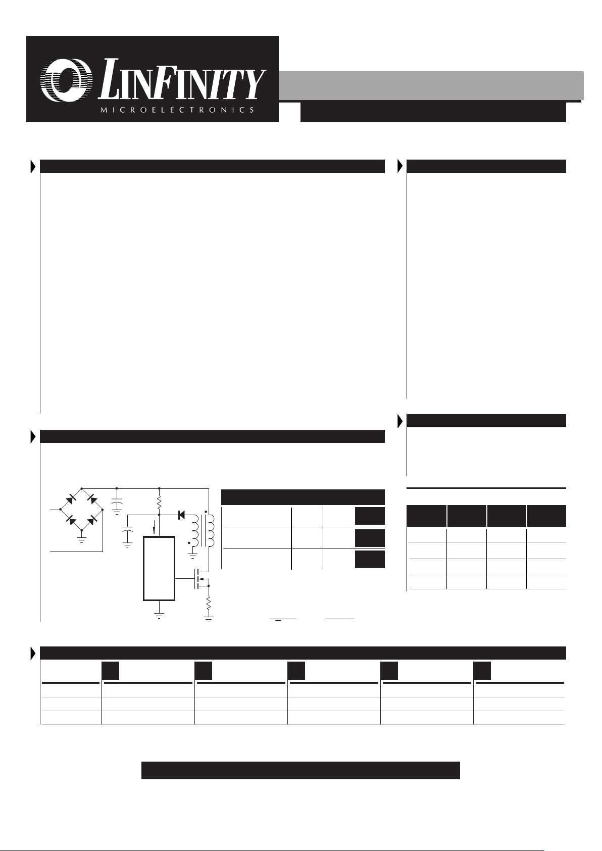
FIGURE 36. — OFF-LINE FLYBACK REGULATOR
7
150k
Ω
100pF
V
FB
COMP
V
REF
RT/C
T
4700µF
10V
5V
2-5A
ISOLATION
BOUNDARY
3600pF
400V
1N4935
820pF
2.5k
Ω
1N4935
IRF830
27k
Ω
0.01µF
10µF
20V
1N4935
1k
Ω
470pF
0.85k
Ω
MBR735TI
4.7k
Ω
2W
250kΩ
1/2W
220µF
250V
4.7
Ω
1W
1N4004
1N40041N4004
1N4004
AC
INPUT
V
CC
OUT
CUR
SEN
GND
LX1554
20k
Ω
3.6k
Ω
10k
Ω
.0022µF0.01µF
16V
3
6
2
1
8
4
5
SPECIFICATIONS
Input line voltage: 90VAC to 130VAC
Input frequency: 50 or 60Hz
Switching frequency: 40KHz ±10%
Output power: 25W maximum
Output voltage: 5V +5%
Output current: 2 to 5A
Line regulation: 0.01%/V
Load regulation: 8%/A*
Efficiency @ 25 Watts,
V
IN
= 90VAC: 70%
V
IN
= 130VAC: 65%
Output short-circuit current: 2.5Amp average
*This circuit uses a low-cost feedback scheme in which the DC
voltage developed from the primary-side control winding is
sensed by the LX1554 error amplifier. Load regulation is
therefore dependent on the coupling between secondary and
control windings, and on transformer leakage inductance.
 Loading...