

Page 1
Overview
The LV3400M is a filter IC designed for FM multiplex
broadcast reception and is used in combination with the
Sanyo LC72700 demodulation/error correction IC. The
adoption of switched capacitor (SCF) technology means
that frequency adjustment is not required and that the
LV3400M provides stable operation.
Functions
• 76 kHz band-pass filter (Gaussian filter)
• 54 kHz high-pass filter
• 125 kHz low-pass filter
• Anti-aliasing filter
• Limiter circuit
Features
• Adjustment-free, due to the use of SCF technology.
• Few external components are required.
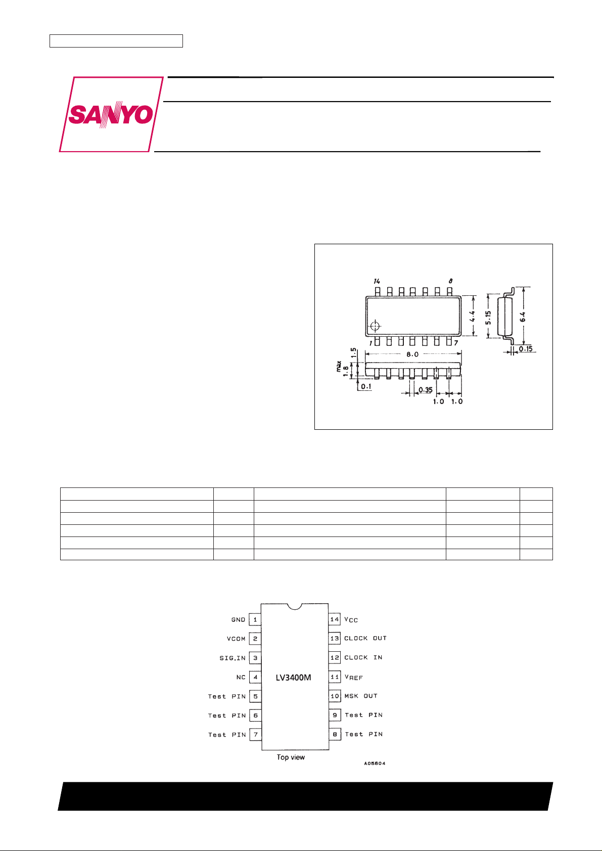
Package Dimensions
unit: mm
3111-MFP14S
Bi CMOS LSI
13096HA (OT)/91295HA (OT)/83194TH (OT) No. 4862-1/4
SANYO: MFP14S
[LV3400M]
SANYO Electric Co.,Ltd. Semiconductor Bussiness Headquarters
TOKYO OFFICE Tokyo Bldg., 1-10, 1 Chome, Ueno, Taito-ku, TOKYO, 110 JAPAN
FM Multiplex Filter
LV3400M
Ordering number : EN4862C
Specifications
Absolute Maximum Ratings at Ta = 25°C
Pin Assignment
Parameter Symbol Conditions Ratings Unit
Maximum supply voltage V
CC
max 6V
Maximum input voltage V
3
, V7, V
12
–0.3 to VCC+ 0.3 V
Allowable power dissipation Pd max 180 mW
Operating temperature Topr –40 to +85 °C
Storage temperature Tstg –55 to +125 °C
Page 2
No. 4862-2/4
LV3400M
Operating Conditions at Ta = 25°C
Operating Characteristics at Ta = 25°C, VCC= 5 V, fCK= 3.6 MHz, VCK= 1 Vp-p
Reference Characteristics
Pin Functions
Usage Notes
1. Pins 4 to 9 and pin 13 are left open in normal use.
2. The clock should be taken from the decoder (LC72700) clock output pin and input to pin through a capacitor of about
100 pF. Spurious radiation from the clock line can be reduced by inserting a resistor in the line and thus smoothing
the rising and falling edges. This signal is then input to pin 12 through a capacitor.
Parameter Symbol Conditions Ratings Unit
Operating supply voltage range V
CC
4.5 to 5.5 V
A composite signal corresponding to a 100%
200 to 300 mVrms
Input signal voltage range V
IN
FM modulation level
f
IN
= 76 kHz, CW 8 to 30 mVrms
Clock frequency f
CK
3.60 MHz
Clock input voltage V
CK
1.0 to V
CC
Vp-p
Parameter Symbol Conditions min typ max Unit
Current drain I
CCO
The pin 14 current for a no-signal input to V
IN
3.8 6 8 mA
SCF block common voltage V
2
The pin 2 voltage for a no-signal input to V
IN
2.1 2.3 2.5 V
Signal input resistance Rin3 The pin 3 input resistance 36 kΩ
Clock input resistance Rin12 The pin 12 input resistance 100 kΩ
[MSK Output]
The input level such that an MSK output with the same
MSK input sensitivity V
3S
frequency is acquired when a 76-kHz CW is applied 4 mVrms
as V
IN
.
MSK output high level V
10H
VIN= 76 kHz, 4 mVrms, CW
4 V
MSK output low level V
10L
0.4 V
Parameter Symbol Conditions Ratings Unit
AAF cutoff frequency 300 kHz
HPF corner frequency 54 kHz
LPF cutoff frequency 125 kHz
BPF center frequency 76 kHz
BPF -3 dB frequency 19 kHz
Maximum in-band group delay time difference ±5 µs
PinNo. Symbol Description
1 GND Ground
2 VCOM SCF block common. A decoupling capacitor must be used.
3 SIG. IN
Signal input. Input an FM modulated signal (composite signal). A modulated signal between 200 and 300 mVrms should be
input. The input sensitivity for a pure 76-kHz signal is 4 mVrms or lower.
10 MSK OUT MSK output (CMOS output)
11 V
REF
Limiter reference voltage. A low-pass filter is formed by the internal resistance (which is about 10 kΩ) and an external capacitor.
12 CLK IN
3.6-MHz clock input. The DC bias at the CMOS inverter input, to which a 100-kΩ feedback resistor is connected, is about
V
CC
/2. The clock signal is input through a capacitor.
13 CLK OUT The clock output that was wave-shaped by an inverter. This pin is normally left open.
14 V
CC
Power supply
4 to 9 NC, Test PIN This pin must be left open.
Page 3

No. 4862-3/4
LV3400M
Test Circuit
Note: Pins 4 to 9 are left open.
Page 4

No. 4862-4/4
LV3400M
This catalog provides information as of December, 1997. Specifications and information herein are subject to
change without notice.
■ No products described or contained herein are intended for use in surgical implants, life-support systems, aerospace
equipment, nuclear power control systems, vehicles, disaster/crime-prevention equipment and the like, the failure of
which may directly or indirectly cause injury, death or property loss.
■ Anyone purchasing any products described or contained herein for an above-mentioned use shall:
➀ Accept full responsibility and indemnify and defend SANYO ELECTRIC CO., LTD., its affiliates, subsidiaries and
distributors and all their officers and employees, jointly and severally, against any and all claims and litigation and all
damages, cost and expenses associated with such use:
➁ Not impose any responsibility for any fault or negligence which may be cited in any such claim or litigation on
SANYO ELECTRIC CO., LTD., its affiliates, subsidiaries and distributors or any of their officers and employees
jointly or severally.
■ Information (including circuit diagrams and circuit parameters) herein is for example only; it is not guaranteed for
volume production. SANYO believes information herein is accurate and reliable, but no guarantees are made or implied
regarding its use or any infringements of intellectual property rights or other rights of third parties.
 Loading...