

Page 1
Ordering number: EN4876B
Bi-CMOS LSI
LV2105V
530 MHz PLL Frequency Synthesizer LSI
Overview
The LV2105V is a PLL frequency synthesizer Bi-CMOS LSI
that provides low-voltage operation and low current drain, and
that is suitable for use in a variety of radio equipment.
Functions
.
PLL function
.
Data input by serial transfer (CCB format)
.
Input amplifier for crystal oscillation circuit
.
Data output port
Features
.
Low operating voltage: (VCC= 2.5 to 5.5 V)
.
Low current drain (5.5 mA)
.
Compact package (SSOP16, 0.65 mm pitch)
.
VCO band switching data output port on chip
.
Data can be input while in power saving mode
.
Data input pin high level can be input at VCCor higher
.
Independent setting of CP ON/OFF (high impedance)
possible
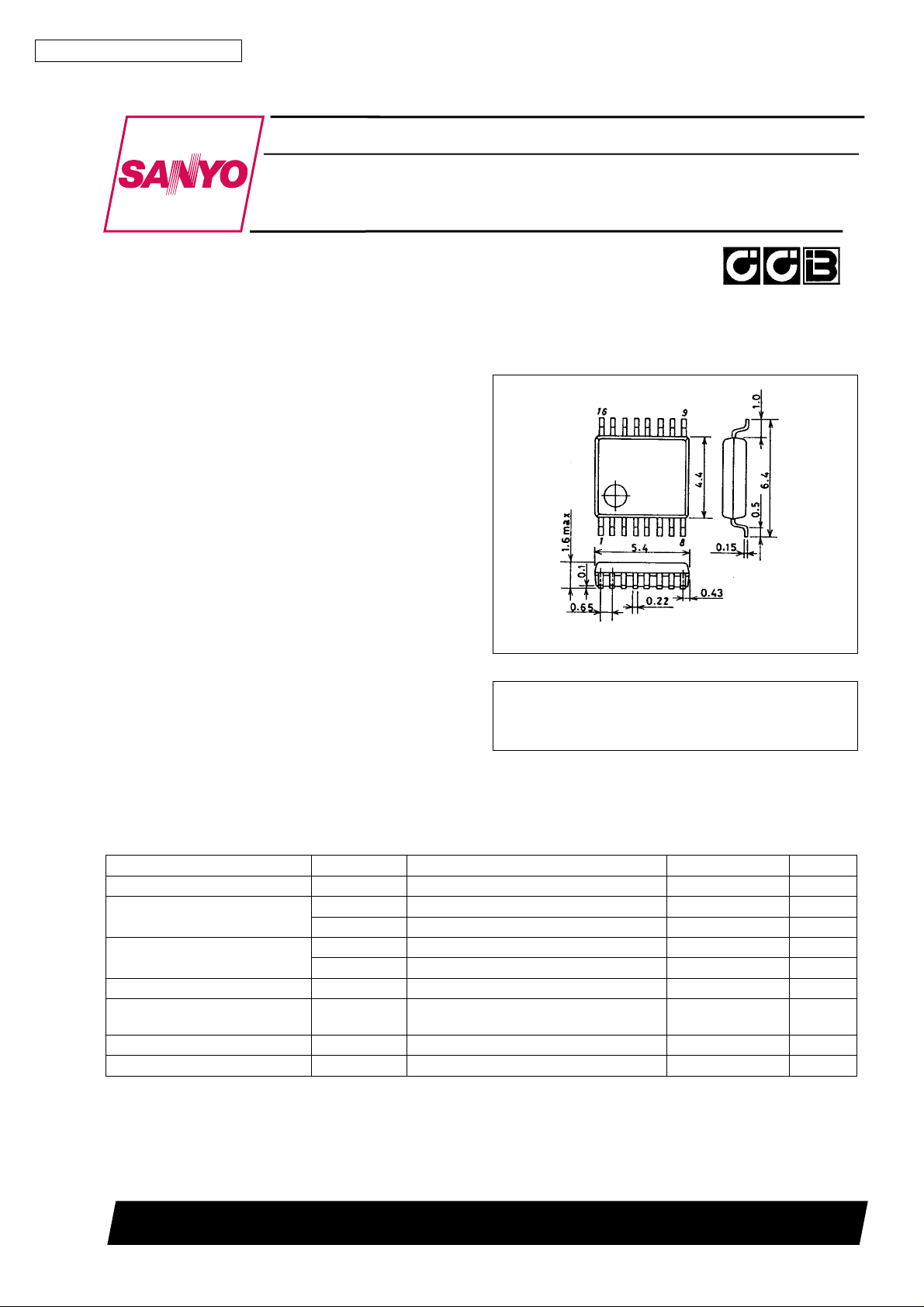
Package Dimensions
unit: mm
3178-SSOP16
[LV2105V]
SANYO : SSOP16
.
CCB is a trademark of SANYO ELECTRIC CO., LTD.
.
CCB is SANYO’s original bus format and all the bus
addresses are controlled by SANYO.
Specifications
Absolute Maximum Ratings atTa=25°C
Parameter Symbol Conditions Ratings Unit
Maximum supply voltage V
Maximum input voltage
Maximum output voltage
Maximum output current I
Allowable power dissipation Pd max
Operating temperature Topr –40 to +85
Storage temperature Tstg –50 to +125
max VCCR, VCCD –0.3 to +6.0 V
CC
V
max(1) CE, CL, DI –0.3 to +6.0 V
IN
V
max(2) XIN, TEST –0.3 to VCC+0.3 V
IN
V
max(1) PDP –0.3 to +9.0 V
OUT
V
max(2) PDN, OUT, PE –0.3 to VCC+0.3 V
OUT
max PDP 0 to +1.0 mA
OUT
114 × 76 × 1.6 mm
When using glass epoxy board
3
SANYO Electric Co.,Ltd. Semiconductor Bussiness Headquarters
TOKYO OFFICE Tokyo Bldg., 1-10, 1 Chome, Ueno, Taito-ku, TOKYO, 110 JAPAN
D3095HA(II) No.4876-1/7
230 mW
°
°
C
C
Page 2

LV2105V
Pin Assignment
Allowable Operating Ranges at Ta = –40 to +85°C
Parameter Symbol Conditions Min Typ Max Unit
Supply voltage V
CC
High-level input voltage V
Low-level input voltage V
Output voltage V
Input frequency
Input amplitude
V
V
f
f
OUT
IN
IN
IN
IN
Crystal oscillation condition Xtal XIN, (XOUT) 5 13 MHz
VCCR, VCCD 2.5 5.5 V
CE, CL, DI VCCR × 0.7 5.5 V
IH
CE, CL, DI 0 +0.6 V
IL
PDP 0 +7.0 V
(1) XIN: Sine wave capacitive coupling 5 22 MHz
(2) PI: Sine wave capacitive coupling 100 530 MHz
(1) XIN: Sine wave capacitive coupling –12 +10 dBm
(2) PI: Sine wave capacitive coupling –18 0 dBm
Electrical Characteristics atTa=25°C, VCCR = 3.0 V, VCCD = 3.0 V
Parameter Symbol
(1) PDP: IO= 0.5 mA 0.5 V
V
OL
V
(2) PDN: IO= 0.5 mA 0.5 V
Low-level output voltage
High-level output voltage
Output off leak current
C.P output current I
High-level input current
Low-level input current
OL
V
(3) PE: IO= 0.5 mA 0.5 V
OL
V
(4) OUT: IO= 2.0 mA 0.5 V
OL
V
(1) PE: IO= –0.5 mA VCC−0.5 V
OH
V
(2) PDN: IO= –0.5 mA VCC−0.5 V
OH
I
(1) PDP: VO= 3.0 V 1.0 µA
OFF
I
(2) CP: VO= 1.5 V 100 nA
OFF
CP
I
H
I
H
I
H
(1) CE, CL, DI: VI= 0 V 5.0 µA
I
L
I
(2) XIN: VI= 0 V 2.3 3.0 4.3 µA
L
I
(3) TEST: VI= 0 V 5.0 µA
L
CP: VO= 1.5 V ±4.0 ±7.5 ±11 mA
(1) CE, CL, DI: VI= 3.0 V 5.0 µA
(2) XIN: VI= 3.0 V 2.3 3.0 4.3 µA
(3) TEST: VI= 3.0 V 5.0 µA
Internal feedback resistance Rf XIN 1.0 MΩ
Supply current I
PS supply current I
(1) VCCR, VCCD: *1 5.5 9.0 mA
CC
(2) VCCR, VCCD: *1 0.4 0.6 mA
CC
*1: XIN = 12.8 MHz, 10 dBm, PI = 400 MHz, 0 dBm, other input pins = 0 V, output, I/O pins = OPEN CP OFF
Conditions
min typ max Unit
No.4876 -2/7
Page 3
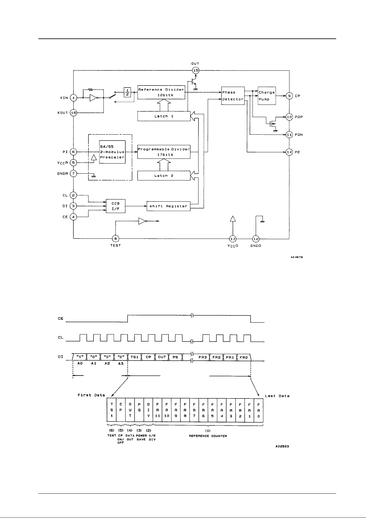
Equivalent Circuit Block Diagram
LV2105V
Serial Data (PLL Control Data) Configuration
1) Mode 1: Latch-1 data (Reference divider, other data)
Mode data
Control data
No.4876 -3/7
Page 4

2) Mode 2: Latch-2 data (Programmable divider data)
LV2105V
Mode data
Serial Data (Transfer) Timing
Control data
Internal data
Serial Data Explanation
Pin No. Control block/data Internal block
(1) Reference frequency data
FR0 to FR1
(2) 1/2 divider data
DIV
.
Data that sets the division ratio of the reference divider.
Binary value with FR0 as the LSB. However, the settable division ratio
factor is up to 4095.
(Actual division ratio) = (Set division ratio)
.
Data that sets whether to use 1/2 DIV or to enter the through state.
DIV data Item
0 Through
1 1/2 DIV
(×2: when DIV is ‘‘1’’)
Continued on next page.
No.4876 -4/7
Page 5

LV2105V
Continued from preceding page.
Pin No. Control block/data Internal block
(3) Power save data
PS
.
Data that sets the power save mode on or off
PS data Item
0 Power save mode
1 Normal operation
(4) Output port data
OUT
(5) Charge pump ON/OFF data
CP
(6) LSI test data TS1
(7) Programmable divider data
FP0 to FP16
.
Data that sets the output of the output port
OUT data OUT Pin
0 Low
1 High
.
Data that sets whether to operate the charge pump or to implement
high impedance.
CP data Item
0 High impedance
1 Normal operation
.
LSI test mode switch.
Set TS1 = 0. Normally, the TEST pin is connected to GND.
.
Data that sets the division ratio of the programmable divider.
Binary value with FP0 as the LSB. However, the settable division ratio
factor is up to 131071.
Pin Functions
Pin Name Pin Function I/O Style
1 XIN Reference signal input pin (Xtal oscillation pin) CMOS input
2 CL Data input pin CMOS, No pull-down
3 DI Data input pin CMOS, No pull-down
4 CE Data input pin CMOS, No pull-down
5V
6 PI Comparison signal input pin BIP input
7 GND R ECL block GND pin
8 TEST LSI test pin. Must be connected to GND. CMOS, No pull-down
9 CP Built-in charge pump output pin BIP
10 PDP Phase comparator output for an external charge
11 PDN Phase comparator output for an external charge
12 GND D GND pin for circuits except the ECL block
13 V
14 PE Phase error output pin for phase comparator CMOS output
15 OUT Output port pin for switching external SW. BIP NPN open-collector output
16 XOUT Output pin for Xtal oscillation CMOS output
R ECL block power supply pin
CC
pump.
If not to be used, connect to GND.
pump.
D Power supply pin for circuits except the ECL block
CC
CMOS, Nch open-drain output
CMOS output
No.4876 -5/7
Page 6

Sample Application Circuit
LV2105V
No.4876 -6/7
Page 7

LV2105V
No products described or contained herein are intended for use in surgical implants, life-support systems, aerospace equipment,
nuclear power control systems, vehicles, disaster/crime-prevention equipment and the like, the failure of which may directly or
indirectly cause injury, death or property loss.
Anyone purchasing any products described or contained herein for an above-mentioned use shall:
1 Accept full responsibility and indemnify and defend SANYO ELECTRIC CO., LTD., its affiliates, subsidiaries and distributors
and all their officers and employees, jointly and severally, against any and all claims and litigation and all damages, cost and
expenses associated with such use:
2 Not impose any responsibility for any fault or negligence which may be cited in any such claim or litigation on SANYO
ELECTRIC CO., LTD., its affiliates, subsidiaries and distributors or any of their officers and employees jointly or severally.
Information (including circuit diagrams and circuit parameters) herein is for example only; it is not guaranteed for volume
production. SANYO believes information herein is accurate and reliable, but no guarantees are made or implied regarding its use
or any infringements of intellectual property rights or other rights of third parties.
This catalog provides information as of December, 1995. Specifications and information herein are subject to change without notice.
No.4876 -7/7
 Loading...