

Page 1
Ordering number :ENN6287
73099RM (OT) No. 6287-1/9
Overview
The LV1150M is a virtual surround system Bi-CMOS IC
for video soundtracks and audio.
The main feature of this IC is the ability to create an audio
ambience equivalent to that of a multichannel system by
adding a signal to which virtual surround processing has
been applied to the left and right channel input signals. It
furthermore allows modification of this effect by the use
of L+R and L–R passive matrix processing and adjustment
of the surround processing level with a level control.
Functions and Features
• Virtual surround function
• Passive matrix: L+R, L–R
• Adjustable surround effect level
• Bypass and virtual surround (L+R, L–R) switching
function
• Output filters are provided on chip.
• On-chip VDDcircuit
• ADM technique based A/D and D/A converters
• Simulated stereo for monaural input signals
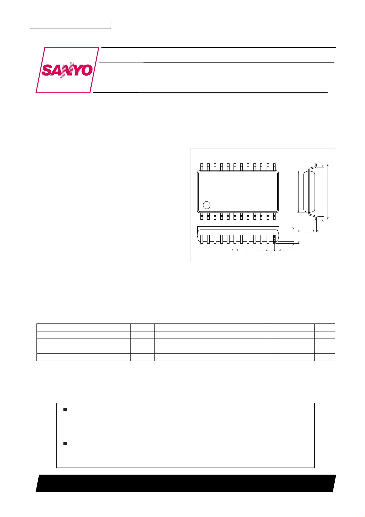
• Package: MFP24 (375-mil lead pitch)
Package Dimensions
unit: mm
3045B-MFP24
0.15
15.3
1
12
24
13
0.67
0.35
1.27
7.9
0.75
9.0
10.5
2.5max
2.150.1
SANYO: MFP24
[LV1150M]
SANYO Electric Co.,Ltd. Semiconductor Company
TOKYO OFFICE Tokyo Bldg., 1-10, 1 Chome, Ueno, Taito-ku, TOKYO, 110-8534 JAPAN
Bi-CMOS IC
LV1150M
Virtual Surround System IC
Any and all SANYO products described or contained herein do not have specifications that can handle
applications that require extremely high levels of reliability, such as life-support systems, aircraft’s
control systems, or other applications whose failure can be reasonably expected to result in serious
physical and/or material damage. Consult with your SANYO representative nearest you before using
any SANYO products described or contained herein in such applications.
SANYO assumes no responsibility for equipment failures that result from using products at values that
exceed, even momentarily, rated values (such as maximum ratings, operating condition ranges, or other
parameters) listed in products specifications of any and all SANYO products described or contained
herein.
Parameter Symbol Conditions Ratings Unit
Maximum supply voltage V
CC
max 12 V
Allowable power dissipation Pdmax Ta ≤ 70°C * With printed circuit board 500 W
Operating temperature Topr –20 to +70 °C
Storage temperature Tstg –40 to +125 °C
Specifications
Absolute Maximum Ratings at Ta = 25°C
Note: * Printed circuit board size: 114.3 × 76.1 mm, t = 1.6 mm. Material: Glass epoxy.
Page 2
No. 6287-2/9
LV1150M
Electrical Characteristics at Ta = 25°C, VCC= 7.0 V, VIN= –10 dBm, f = 1 kHz, in bypass mode
Parameter Symbol Conditions Ratings Unit
Recommended supply voltage V
CC
7V
Operating supply voltage range V
CC
opr 6.5 to 10 V
Operating Conditions at Ta = 25°C
Parameter Symbol Conditions
Ratings
Unit
min typ max
Quiescent current I
CC
15 23 40 mA
Output noise voltage V
NO
Rs = 10 kΩ, JIS A –110 –90 dBm
In virtual surround mode –88 –80 dBm
I/O signal level deviation V
O
VIN= –10 dBm = 0 dB –2 0 +2 dB
Total harmonic distortion THD
400 Hz to 30 kHz bandpass filter 0.005 0.03 %
In virtual surround mode 0.13 1.0 %
Headroom H • R
V
IN
= –10 dBm = 0 dB, THD = 1% 10 15 dB
In virtual surround mode 10 12 dB
Page 3
No. 6287-3/9
LV1150M
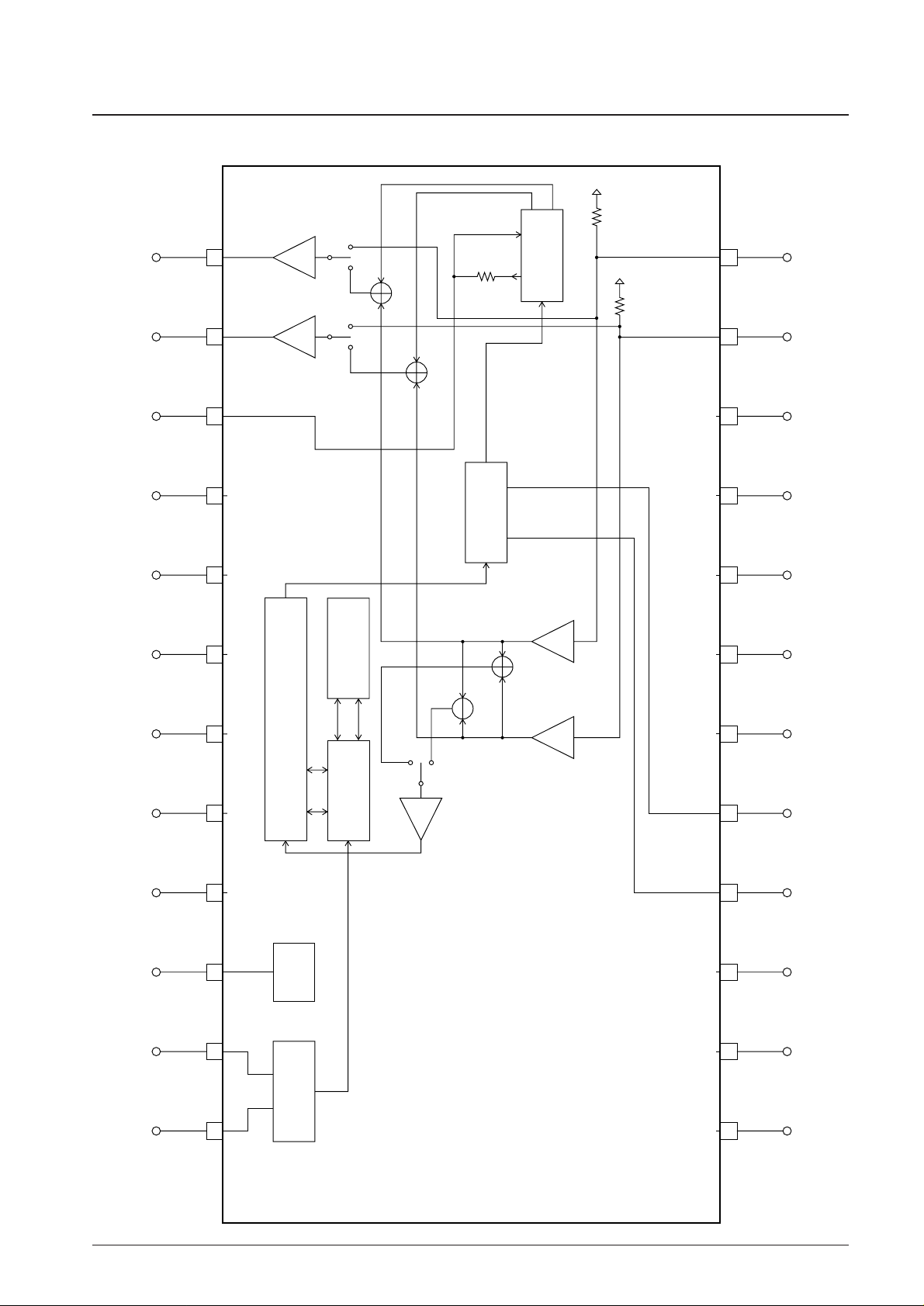
Block Diagram
1 2 3 4 5 6 7 8 9 10 11 12
24 23 22 21 20 19 18 17 16 15 14 13
OSC
ADM
ADM-CONT
V
DD
SRAM
L.P.F.
VIRTUAL
A
B
AB
L – R
L + R
L + DELAY
R + DELAY
AB
50 kΩ
2 kΩ
50 kΩ
V
SS
SW1 SW2 LPF1 LPF2 LS-OUT R-PS-IN V
CC
L-PS-IN RS-OUT L-IN R-IN
R-OUTL-OUTEF-VOL
V
REF
AGNDDC-CUTD/ANSA/D
V
DD
LC-INBLC-INE
A12415
Page 4

No. 6287-4/9
LV1150M
Test Circuit
1 2 3 4 5 6 7 8 9 10 11 12
24 23 22 21 20 19 18 17 16 15 14 13
V
SS
V
CC
AGND V
REF
OSC
ADM
ADM-CONT
V
DD
SRAM
L.P.F.
VIRTUAL
A
B
SW1
A
B
L – R
L + R
L + DELAY
R + DELAY
AB
50 kΩ
2 kΩ
50 kΩ
130 pF
75 pF
+
+
+
+
+
+
220 µF
0.1 µF
0.15 µF 1.5 kΩ
+
OPEN/5 V-BYPASS
GND-VIRTUAL
BYPASS/VIRTUAL
OPEN/5 V-L–R
GND-L+R
1 µF
1 µF
R-OUT
+
220 µF
0.33 µF
0.15 µF
3300 pF
0.15 µF
220 µF
0.1 µF
100 pF
47 pF
15 pF
51 pF
10 µH
L-OUT
A
B
SW2
SW8
L+R/L–R
0.15 µF1.5 kΩ
+
1 µF
10 kΩ
+
A
B
SW9
A12416
10 kΩ
A
B
1 µF
B
A
Page 5

Sample Application Circuit
No. 6287-5/9
LV1150M
1 2 3 4 5 6 7 8 9 10 11 12
24 23 22 21 20 19 18 17 16 15 14 13
V
SS
V
CC
AGND
V
REF
OSC
ADM
ADM-CONT
V
DD
SRAM
L.P.F.
VIRTUAL
A
B
AB
L – R
L + R
L + DELAY
R + DELAY
A
B
50 kΩ
2 kΩ
9.4 kΩ
REF
REF
REF
REF
50 kΩ
7 96 10
2-6 kΩ
20 kΩ
10 kΩ
SAMP2
1.5 kΩ
0.1 µF-0.22 µF
REF
7 96 10
0-3 kΩ
20 kΩ
10 kΩ
SAMP1
1.5 kΩ
0.1 µF-0.22 µF
130 pF
75 pF
+
+
+
+
+
+
1 µF
220 µF
0.1 µF
L-IN
SAMP1, 2SAMP1, 2
+
R-IN
2.5VPP-
–50 kΩ
OPEN/5 V-BYPASS
GND-VIRTUAL
OPEN/5 V-L–R
GND-L+R
BYPASS
L+R/L–R
10 µF
R-OUT
+
VOL
220 µF
0.33/1 µF
0.15 µF
VOL
3300 pF
0.15 µF
220 µF
0.1 µF
100 pF
47 pF
15 pF
51 pF
5.6-10 µH
L-OUT
A12417
10 µF
1 µF
Page 6

No. 6287-6/9
LV1150M
Operating Principles
1. Modes
The mode can be set using DIP switches on pins 2 and 3.
• Bypass/virtual: switches between bypass and virtual modes.
• L+R/L–R: Switches the virtual mode effect.
Since this switching is independent of the bypass function, it has no effect in bypass mode.
2. Other notes
• The level of the virtual effect can be changed by the values of the external resistors connected to pins 15 and 19.
(See the sample application circuit diagram.) Note that the effect is maximum when these pins are open.
• There are two options that may be attached to pins 6 and 7 and pins 9 and 10. (See the sample application circuit
diagram.) High boost (SAMP1) and low boost (SAMP2) effects can be acquired using external circuits on these
pins. (See the charts.)
–10
–15
–5
0
–10
–15
–5
0
–5
–10
0
5
–5
–10
0
5
2 3 5 7 100
2
357
1k
52 3 7 10k 32 2 3 5 7 100
2
357
1k
52 3 7 10k 32
L→L
R→R
R→L
L
→
R
L→L
R→R
R→L
L
→
R
L → R/R → L — dB
L → R/R → L — dB
L → L/R → R — dB
L→L/R→R — dB
VO — f
IN
VO — f
IN
LV1150M SAMP1
DELAY = OFF
300 mV = 0 dB
LV1150M SAMP2
DELAY = OFF
300 mV = 0 dB
20 kΩ
external
10 kΩ
1.5 kΩ
0.15µF
1.5 kΩ
20 kΩ
–
+
external
10 kΩ
3 kΩ
0.15µF
1.5 kΩ
(19 PIN ⇔ 16PIN Short)
(19 PIN ⇔ 16PIN Short)
Input frequency, fIN— Hz
Input frequency, fIN— Hz
Pin Descriptions
Pin No. Pin Pin voltage (V) Function Equivalent circuit
2
SW1
2
3
1 kΩ
A12418
Bypass/virtual switching
4
5
LPF1
LPF2
Low-pass filter capacitor connection
1/2V
CC
6
10
LS-OUT
RS-OUT
BIAS
4
5
24 kΩ 500 Ω
A12419
Surround signal outputs
0/0.7
7
9
R-PS-IN
L-PS-IN
1/2V
CC
1/2V
CC
Virtual surround processing signal inputs.
6
10
BIAS
100 Ω
V
CC
A12420
7
9
500 Ω
1.5 kΩ
A12421
3 SW1 L+R/L–R switching
Continued on next page.
Page 7

No. 6287-7/9
LV1150M
Continued from preceding page.
Pin No. Pin Pin voltage Function Equivalent circuit
11
12
L-IN
R-IN
11
12
500 Ω
50 kΩ
A12422
Signal inputs
13
14
R-OUT
L-OUT
Signal outputs
1/2V
CC
15
EF-VOL
15
500 Ω
2 kΩ
A12424
Virtual surround control
1/2V
CC
16
V
REF
V
CC
16
3 kΩ
3 kΩ
A12425
V
REF
amplifier reference
1/2V
CC
18
DC-CUT
DC cut capacitor connection
19
21
23
24
D/A
A/D
LC-INB
LC-INE
Clock control
9.4 kΩ
19
20
500 Ω
A12427
A/D (D/A) converter integrator capacitor
connection
1/2V
CC
20
NS
1/2V
CC
A/D noise shaper capacitor connection
13
14
BIAS
100 Ω
V
CC
A12423
18
500 Ω
20 kΩ
20 kΩ
A12426
20
500 Ω
10 kΩ
A12428
23
500 Ω
15 kΩ
24
A12429
0/5V
1/2V
CC
1/2V
CC
Page 8

No. 6287-8/9
LV1150M
–20
–10
0
10
2 3 5 7 100 2 3 5 7 1k 2 3 5 7 10k 2 3
2
5
7
0.1
3
5
7
1.0
2
3
5
7 100 2 3 5 7 1k 2 3 5 7 10k
–89
–88
–87
–86
–85
5768910111213
11
10
12
13
567
8
910 1211 13
V
O(DELAY)
— f
IN
V
CC
= 7 V
V
IN
= –10 dBm = 0 dB
VIRTUAL L–R mode
V
CC
= 7 V
VIRTUAL L–R mode
RS = 10 kΩ
JIS-A
V
CC
= 7 V
V
IN
= –8.3 dBm = 0 dB
VIRTUAL L+R mode
V
CC
= 7 V
VIRTUAL L–R mode
f
IN
= 1 kHz
THD ≤ 1%
–10 dBm = 0 dB
V
CC
= 7 V
V
IN
= –10 dBm
VIRTUAL L–R mode
400 to 30 kHz BPF
VNO(DELAY) — V
CC
THD(DELAY) — f
IN
VO(L-OUT) — f
IN
–12
–9
–6
–3
0
3
6
–15
9
2 3 5 7 100 2 3 5 7 1k 2 3 5 7 10k 2
H • R(DELAY) — V
CC
V
CC
= 7 V
V
IN
= –8.3dBm = 0 dB
VIRTUAL L+R mode
VO(R-OUT) — f
IN
–12
–9
–6
–3
0
3
6
–15
9
2 3 5 7 100 2 3 5 7 1k 2 3 5 7 10k 2
–91
–92
–90
–89
–88
–87
5678910111213
–112.2
–112.0
–111.8
–111.6
–111.4
–111.2
–111.0
–110.8
5 6 7 8 9 10111213
L-OUT
R-OUT
VNO — V
CC
VNO — V
CC
V
CC
= 7 V
VIRTUAL L + R mode
RS = 10 kΩ
JIS-A
V
CC
= 7 V
BYPASS mode
RS = 10 kΩ
JIS-A
L→L
R→R
Delay output voltage, V
O
— dB
Delay signal total harmonic distortion, THD — %Delay headroom, H • R — dB
Input frequency, fIN— Hz
Supply voltage, VCC— V
Supply voltage, VCC— V
Input frequency, fIN— Hz
Input frequency, f
IN
— Hz
Left and right channel
common-mode input
Supply voltage, VCC— V
Supply voltage, V
CC
— V
Input frequency, f
IN
— Hz
Delay output noise voltage, V
NO
— dBm
Output voltage, V
O
— dB
Output voltage, V
O
— dB
Output noise voltage, V
NO
— dB
Output noise voltage, V
NO
— dB
Left input
Right input
Left input
Right input
Right input
Left input
Left and right channel
common-mode input
Page 9

PS No.6287-9/9
LV1150M
This catalog provides information as of July, 1999. Specifications and information herein are subject to
change without notice.
Specifications of any and all SANYO products described or contained herein stipulate the performance,
characteristics, and functions of the described products in the independent state, and are not guarantees
of the performance, characteristics, and functions of the described products as mounted in the customer’s
products or equipment. To verify symptoms and states that cannot be evaluated in an independent device,
the customer should always evaluate and test devices mounted in the customer’s products or equipment.
SANYO Electric Co., Ltd. strives to supply high-quality high-reliability products. However, any and all
semiconductor products fail with some probability. It is possible that these probabilistic failures could
give rise to accidents or events that could endanger human lives, that could give rise to smoke or fire,
or that could cause damage to other property. When designing equipment, adopt safety measures so
that these kinds of accidents or events cannot occur. Such measures include but are not limited to protective
circuits and error prevention circuits for safe design, redundant design, and structural design.
In the event that any or all SANYO products (including technical data, services) described or contained
herein are controlled under any of applicable local export control laws and regulations, such products must
not be exported without obtaining the export license from the authorities concerned in accordance with the
above law.
No part of this publication may be reproduced or transmitted in any form or by any means, electronic or
mechanical, including photocopying and recording, or any information storage or retrieval system,
or otherwise, without the prior written permission of SANYO Electric Co., Ltd.
Any and all information described or contained herein are subject to change without notice due to
product/technology improvement, etc. When designing equipment, refer to the “Delivery Specification”
for the SANYO product that you intend to use.
Information (including circuit diagrams and circuit parameters) herein is for example only; it is not
guaranteed for volume production. SANYO believes information herein is accurate and reliable, but
no guarantees are made or implied regarding its use or any infringements of intellectual property rights
or other rights of third parties.
Input frequency, fIN— Hz
Supply voltage, VCC— V
Input frequency, fIN— Hz
Output voltage, V
O
— dB
Total harmonic distortion, THD — %
Headroom, H • R — dB
0.01
2
7
5
3
2
THD — f
IN
L→L
R→R
V
= 7 V
CC
V
= –10 dBm
IN
BYPASS mode
400 to 30 kHz BPF
0.001
2 3 5 7 1k 2 3 5 7 10k 2 3 5
22
V
= 7 V
CC
BYPASS mode
f
= 1 kHz
IN
THD ≤ 1%
20
–10 dBm = 0 dB
18
16
H • R — V
CC
0.2
0
–0.2
–0.4
–0.6
–0.8
V
= 7 V
CC
V
= –10 dBm = 0 dB
IN
BYPASS mode
–1.0
2 3 5 7 100 2 3 5 7 1k 2 3 5 7 10k 2 3
VO — f
L→L
R→R
IN
14
57681091211 13
 Loading...