

Page 1
Data Sheet
April 1999
W3030 3 V Dual-Mode IF Cellular Receiver
Features
n Proven double conversion architecture:
First IF capability: 10 MHz to over 1000
MHz
Second IF capability: 0.2 MHz to 2.0 MHz
n Dual second IF amplifiers and demodulators:
Analog-mode limiting amplifier and FM
quadrature detector
Digital-mode linear AGC amplifiers with
dual-mixer I & Q quadrature demodulator
n Accurate, onboard local oscillator phase splitter
for digital quadrature demodulator
n Four enable/powerdown modes, selectable from
two digital control pins, allow operation with
minimal supply current
VCC
GND
ENBA
ENBD
VCM
AGC
LOGIC AND
BIAS
CONTROL
DIGITAL SECTION
VARIABLE GAIN
n Low supply current
n Analog received signal strength indicator (RSSI)
available
n Analog AGC for digital-mode IF amplifiers
n Over 100 dB combined voltage gain
Applications
n IS-136 (North American dual-mode) cellular
radio portable and mobile terminals
n Cellular radio base stations
n Digital satellite communications
n Multisymbol signaling receivers
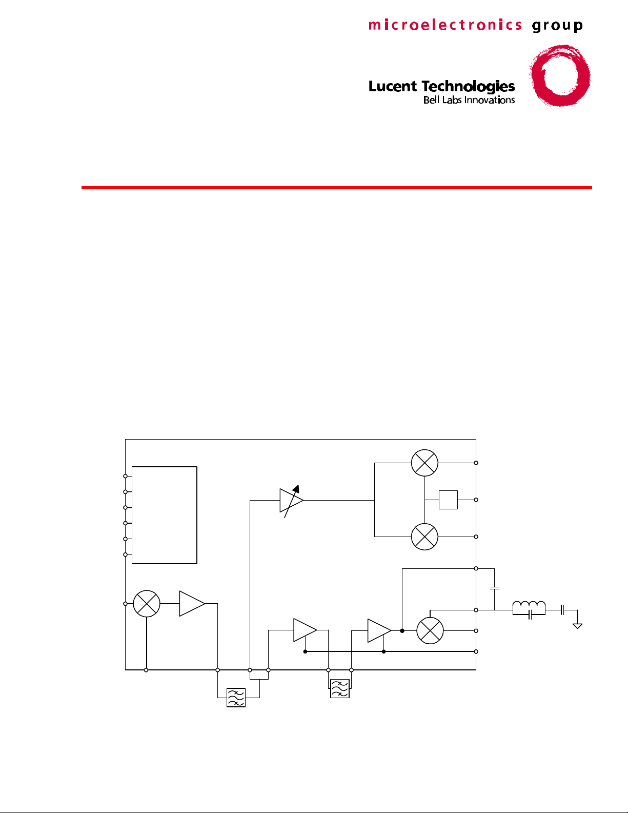
I
÷4
CLK
Q
IF INPUT
ANALOG SECTION
AUDIO
RSSI
LO
Figure 1. General Block Diagram
Page 2

Data Sheet
W3030 3 V Dual-Mode IF Cellular Receiver April 1999
Table of Contents
Features............................................................................................................................................................... 1
Applications .........................................................................................................................................................1
Description...........................................................................................................................................................3
Pin Information.....................................................................................................................................................5
Absolute Maximum Ratings.................................................................................................................................. 7
Handling Precautions...........................................................................................................................................7
Operating Ranges................................................................................................................................................8
Electrical Specifications ....................................................................................................................................... 8
RSSI..................................................................................................................................................................11
Quadrature Detector........................................................................................................................................... 11
Quad Tank S-Curves......................................................................................................................................12
Test Circuit Diagram ..........................................................................................................................................14
Characteristic Curves......................................................................................................................................... 15
Outline Diagram................................................................................................................................................. 20
32-Pin TQFP ......................................................................................................................................................20
Manufacturing Information ................................................................................................................................. 21
Ordering Information..........................................................................................................................................21
Lucent Technologies Inc.2
Page 3

Data Sheet
April 1999 W3030 3 V Dual-Mode IF Cellular Receiver
Description
The W3030 is a monolithic integrated circuit that
provides most of the receive path functions required
to meet the IS-136 (and IS-54) standard. The W3030
converts FM or digitally modulated IF carriers up to
200 MHz and provides required IF gain and separate
baseband detectors for the two modulation modes.
The W3030 is organized into three subfunctions (see
Figure 2):
1. First IF mixer/amplifier
2. Analog second IF
3. Digital second IF sections
(Note that the electrical specification tables
correspond to each subfunction.)
Each section has a buffered output to allow for
external filtering, which also provides flexibility in
system architecture selection. The first IF mixer
section provides 30 dB of fixed voltage conversion
gain (power gain = 17 dB). The first IF mixer also
performs down-conversion to the 0.2 MHz—2.0 MHz
range, which allows the use of inexpensive ceramic
filters at two points in the signal path. In the second IF
section, the signal path may be split between two
parallel amplifier/demodulator sections. In the analog
second IF, there is a 40 dB amplifier followed by a
60 dB hard-limiting amplifier and an FM quadrature
detector (noncoherent discriminator). The signal path
between the 40 dB and 60 dB amplifier stages is
brought off-chip for external filtering purposes. In
digital mode, an AGC amplifier provides gain between
10 dB and 80 dB. The digital signal is demodulated in
double-balanced mixers that are fed with an external
local oscillator (LO) signal. The external LO passes
through a divide-by-four counter to provide the final IF
LO frequency. This architecture greatly reduces the
possibility of feedback of the external LO signal to the
IF input, which would cause dc offsets at the I & Q
outputs. This circuit also provides a 90° phase shift of
the LO that is independent of duty cycle. The resulting
I & Q differential pairs can be level-shifted using the
VCM input pin, providing flexibility in interfacing to
digital processing ICs.
A pair of logic inputs allows the device to be put into a
powerdown mode and one of two partially enabled
modes (analog or digital only), or a fully enabled
mode, allowing the use of analog RSSI while in digital
receive mode.
Lucent Technologies Inc. 3
Page 4

Data Sheet
IF
IF
IF
W3030 3 V Dual-Mode IF Cellular Receiver April 1999
Description (continued)
RSSI
AUDIO
QUAD
IFAOUT
IFAACG
IFAIN
1
FM
DEMOD &
RSSI
2
3
49 kΩ
4
5
1 kΩ
6
GND2
32 31 30 29 28 27 26 25
IFDIN
IFDIN
50 kΩ
ANALOG SECOND
IFDACG
AGC AMP I/Q DEMODULATOR
IF LIMITER
VCM
2 kΩ
AGC
50 kΩ
48 kΩ
FIRST IF MIXER/AMPLIFIER
10 MHz—1000 MHz
I
I
÷
4
24
23
22
21
20
19
CLK
Q
Q
ENBA
ENBD
IF1IN
IFAIN
VCC2
7
8
1 kΩ
9 10 11 12 13 14 15 16
2OUT
50 kΩ
48 kΩ
2ACG
SECOND IF AMP
0.2 MHz—2.0 MHz
2 kΩ
IF2IN
1 kΩ
IF2IN
GND1
1OUT
IF1LO
IF1LO
18
17
IF1IN
VCC1
Figure 2. Detailed Block Diagram with Pinout
Lucent Technologies Inc.4
Page 5

Data Sheet
April 1999 W3030 3 V Dual-Mode IF Cellular Receiver
Pin Information
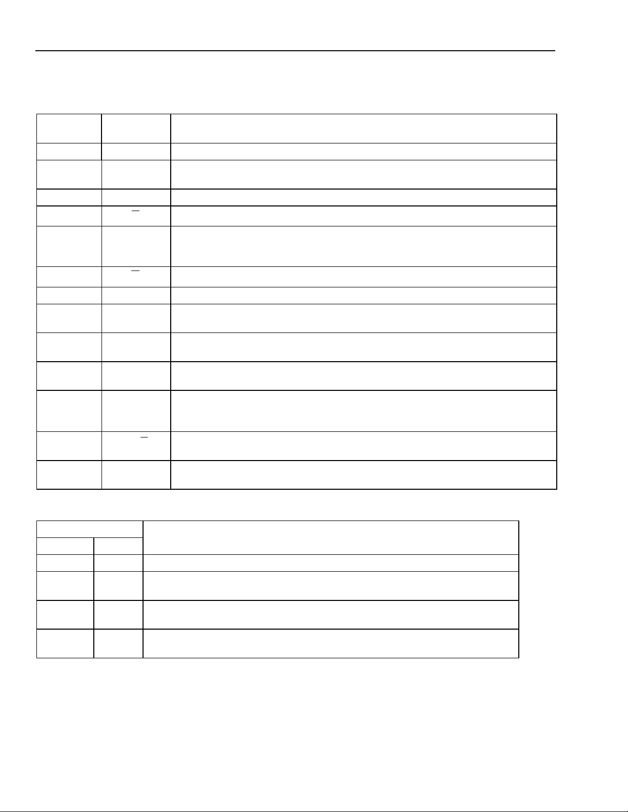
Table 1. Pin Descriptions
Pin
Number
1 RSSI
2 AUDIO
3 QUAD
4 IFAOUT
5 IFAACG
6 IFAIN
7
8 VCC2
9 IF2OUT
10 IF2ACG
11 IF2IN
12
13 GND1
14 IF1OUT
15
16 IF1LO
17 VCC1
18
19 IF1IN
Pin Name Pin Description
IFAIN
IF2IN
IF1LO
IF1IN
Received Signal Strength Indicator. Provides logarithmic (dB-linear) dc output
voltage.
Audio Output. Audio output of FM detector.
Quad Input. Input to FM detector from parallel LC quad coil.
Analog Output. Output of analog section limiting amplifiers; couple to quad coil
and pin 3 (QUAD) with 10 pF capacitor.
Analog Signal Ground. Signal ground for analog section limiting amplifier;
connect to ground with 0.1 µF capacitor.
Analog Mode Limiter Input. Differential input to analog IF limiting amplifier; to
be directly coupled to dielectric sources such as ceramic filters. Pin 6 is
approximately 1 kΩ with pin 5 ac-grounded.
Analog Mode Limiter Input (Inverting). Differential input to analog IF limiting
amplifier. To be ac-grounded.
Second IF Power Supply. Positive power supply connection for both analog
and digital second IF amplifiers and demodulators.
Second IF Output. Output of 40 dB second IF amplifier; directly couple to
dielectric loads such as ceramic filters. Includes internal 1 kΩ termination
resistor.
Second IF Signal Ground. Signal ground for 40 dB second IF amplifier;
connect to ground with 0.1 µF capacitor.
Second IF Input. Differential input to 40 dB second IF amplifier; to be directly
coupled to dielectric sources such as ceramic filters. Pin 11 is approximately
2 kΩ with pin 10 ac-grounded.
Second IF Input (Inverting). Differential input to 40 dB second IF amplifier. To
be ac-grounded.
First IF Mixer Ground. Power supply (dc) ground for first IF mixer section.
First IF Mixer Output. Output of first IF mixer/amplifier section; to be directly
coupled to dielectric loads such as ceramic filters. Includes internal 1 kΩ
termination resistor.
First IF Mixer Logical Input (Inverting). Differential input to first IF mixer local
oscillator; to be capacitively coupled to sources with a dc level offset.
First IF Mixer Logical Input. Differential input to first IF mixer local oscillator.
To be ac-grounded.
First IF Mixer Power Supply. Positive power supply connection for first IF
mixer/amplifier section.
First IF Mixer Input (Inverting). Differential input to first IF mixer/amplifier
section; to be ac-coupled to ground or source.
First IF Mixer Input. Differential input to first IF mixer/amplifier section.
Lucent Technologies Inc. 5
Page 6
Data Sheet
W3030 3 V Dual-Mode IF Cellular Receiver April 1999
Pin Information (continued)
Table 1. Pin Descriptions (continued)
Pin
Number
20 ENBD
21 ENBA
22 Q
23
24 CLK
25
26 I
27 AGC
28 VCM
29 IFDACG
30 IFDIN
31
32 GND2
Pin Name Pin Description
Q
I
IFDIN
Enable Digital Mode. Positive logic enable connection for digital mode operation.
Enable Analog Mode. Positive logic enable connection for analog mode
operation.
Q Output. Differential output from Q mixer of quadrature demodulator.
Q Output (Inverting). Differential output from Q mixer of quadrature demodulator.
Clock Input. Local oscillator (clock) input to quadrature demodulator phase shifter;
to be capacitively coupled. Input frequency must be four times second IF center
frequency.
I Output (Inverting). Differential output from I mixer of quadrature demodulator.
I Output. Differential output from I mixer of quadrature demodulator.
Automatic Gain Control. AGC control input; to be connected to dc source of
0.25 V—1.55 V.
Common-Mode Voltage. Common-mode voltage dc offset set point for I & Q
interface, typically VCC/2.
Digital Signal Ground. Signal ground for digital section limiting amplifier; connect
to ground with 0.1 µF capacitor.
Digital Second IF Input. Differential input to digital section AGC amplifier; to be
directly coupled to dielectric sources such as ceramic filters. Pin 30 is
approximately 2 kΩ with pin 29 ac-grounded.
Digital Second IF Input (Inverting). Differential input to digital section AGC
amplifier. To be ac-grounded.
Second IF Ground. Power supply ground for both analog and digital second IF
amplifier and demodulator sections.
Table 2. Digital Control Pin Truth Table
Control Pin Mode/Function
ENBA ENBD
LOW LOW
LOW HIGH
HIGH LOW
HIGH HIGH
All Sleep. All receive circuits powered down, supply current <10 µA.
Digital Receive. First IF mixing stage, AGC amp and I/Q quadrature
demodulators active.
Analog/FM Receive. First IF mixing stage, 40 dB IF amp, 60 dB limiting amp,
RSSI, and FM detector active.
All Active. All receive circuits functional, e.g., digital mode I & Q demodulator
used with analog RSSI.
Lucent Technologies Inc.6
Page 7

Data Sheet
April 1999 W3030 3 V Dual-Mode IF Cellular Receiver
Absolute Maximum Ratings
Stresses in excess of the absolute maximum ratings can cause permanent damage to the device. These are
absolute stress ratings only. Functional operation of the device is not implied at these or any other conditions in
excess of those given in the operations sections of the data sheet. Exposure to absolute maximum ratings for
extended periods can adversely affect device reliability.
Parameter Min Max Unit
Ambient Operating Temperature –35 100 °C
Storage Temperature –65 150 °C
Lead Temperature (soldering, 10 s) — 300 °C
Positive Supply Voltage 0 4.5 Vdc
Power Dissipation — 650 mW
Output Current (continuous) — 160 mA
ac Peak-to-peak Input Voltage 0 VCC Vdc
Enable Input Voltage –0.3 VCC + 0.4 Vdc
VCM, AGC Input Voltage –0.3 VCC + 0.4 Vdc
Handling Precautions
Although protection circuitry has been designed into this device, proper precautions should be taken to avoid
exposure to electrostatic discharge (ESD) during handling and mounting. Lucent Technologies Microelectronics
Group employs a human-body model (HBM) and a charged-device model (CDM) for ESD-susceptibility testing
and protection design evaluation. ESD voltage thresholds are dependent on the circuit parameters used to define
the model. No industry-wide standard has been adopted for CDM. However, a standard HBM (resistance =
1500 Ω, capacitance = 100 pF) is widely used and, therefore, can be used for comparison purposes. The HBM
ESD threshold presented here was obtained by using these circuit parameters:
W3030 ESD Threshold Voltage
ESD Model Rating
HBM
CDM
≥1500 V
≥1500 V
Lucent Technologies Inc. 7
Page 8

Data Sheet
W3030 3 V Dual-Mode IF Cellular Receiver April 1999
Operating Ranges
Performance is not guaranteed over the full range of all conditions possible within this table. However, this table
lists the ranges of external conditions in which the W3030 provides general functionality, which may be useful in
specific applications, without risk of permanent damage. The conditions for guaranteed performance are
described below.
Table 3. W3030 Operating Ranges
Parameter Min Max Unit
Supply Voltage 2.7 4.1 Vdc
First IF Mixer/Amplifier Section:
Input Frequency Range
LO Frequency
LO Input Level Range
Digital Second IF Amplifier, AGC Quadrature Demodulator Section:
Second IF Frequency
Quadrature Demodulator LO (CLK) Frequency
CLK Input Level (square wave)
Analog Second IF Amplifier Frequency 0.1 4 MHz
VCM Input Range 1.25 VCC – 0.8 V
10
10
–10
0.1
0.4
–10
1000
1000
6
4
16
6
MHz
MHz
dBm/50 Ω
MHz
MHz
dBm/50 Ω
Electrical Specifications
The following apply to all specifications, unless otherwise listed: TA = 25 °C ± 3 °C; VCC = 2.7 Vdc;
PIF1LO = –3 dBm to +3 dBm/50 Ω; IF1 = 10 MHz to 200 MHz; IF2 = 0.2 MHz to 2 MHz; ENBA = ENBD > 1.9 Vdc.
Table 4. dc and Logic Parameters
Parameter Min Typ Max Unit
Supply Current:
Fully Enable (VCC = 3.3)
Analog Only Mode (VCC = 3.3)
Digital Only Mode (VCC = 3.3)
Sleep Mode (VCC = 3.3)
VIHMIN
VILMAX
IILMAX (VI = 0.7 V) — 0 10 µA
IIHMAX (VI = VCC) — 30 250 µA
Enable Time (external capacitor dependent) — 30 — µs
—
—
—
—
1.9 — — V
— — 0.7 V
8
5
5
<1
11
8
8
10
mA
mA
mA
µA
Lucent Technologies Inc.8
Page 9

Data Sheet
April 1999 W3030 3 V Dual-Mode IF Cellular Receiver
Electrical Specifications (continued)
Table 5. First IF Mixer/Amplifier Section
IF deviation = ≤0.5 MHz.
Parameter Min Typ Max Unit
Voltage Gain (with input matching network from 50 Ω source)
Power Gain — 17 — dB
Gain Flatness within IF Deviation — ±0.2 — dB
Noise Figure at IF Input (SSB) — 14 — dB
1 dB Compression Point at Input to Matching Network — –27 — dBm
IP3 at First IF Matching Network Input — –17 — dBm
IF Input Impedance @ 82 MHz — 1.7 II 1.8 —
LO Input Impedance @ 82 MHz — 4 II 1.5 —
IF Output Impedance — 1.0 —
LO Suppression at IF Input (relative to LO input level) — 40 — dB
— 30 — dB
kΩ II pF
kΩ II pF
kΩ
Table 6. Analog Second IF Amplifier, Limiter, RSSI, FM Detector Section
Filter ZIN = ZOUT = 1.0 kΩ; 6 dB attenuation between 40 dB amplifier output and 60 dB limiting amplifier input;
1 kHz FM at 8 kHz deviation; IF filter bandwidth = 28 kHz. Quad tank Q = 10.
Parameter Min Typ Max Unit
IF Gain (net) IF2IN to Audio — 86 — dB
RSSI Range of Input Signal 65 90 — dB
RSSI Output Voltage with –20 dBm/50 Ω into IF1IN
RSSI Output Voltage with –110 dBm/50 Ω into IF1IN
RSSI Linearity over –100 dBm to –35 dBm into IF1IN — ±0.8 ±2.5 dB
RSSI Transfer Function 13 17 25 mV/dB
RSSI Current Capability — 100 — µA
IF Input Impedance (40 dB amplifier) — 2 —
IF Output Impedance (40 dB amplifier) — 1 —
IF Input Impedance (60 dB limiter) — 1 —
IF Output Impedance (60 dB limiter) — 1 —
IP3 of 40 dB Amplifier Section (at its output) — 3 — dBm
FM Detector Input Impedance (quad, pin 3) — 40 —
Audio Output Impedance — 500 —
Audio Output Amplitude (IF1IN = –35 dBm) 150 220 270 mVrms
Audio SINAD for IF1IN = –35 dBm (C-message weighting filter) 32 — — dB
1.75 2.1 2.6 V
0.4 0.7 0.92 V
kΩ
kΩ
kΩ
kΩ
kΩ
Ω
Lucent Technologies Inc. 9
Page 10

Data Sheet
W3030 3 V Dual-Mode IF Cellular Receiver April 1999
Electrical Specifications (continued)
Table 7. Digital Second IF Amplifier, AGC, Quadrature Demodulator Section
PCLK = 320 mVp-p to 640 mVp-p (square wave); IF deviation = ≤0.5 MHz; VCM = 1.3 Vdc to VCC – 0.8 Vdc.
Parameter Min Typ Max Unit
IF Input Impedance — 2 —
CLK Input Impedance — 28 II 8.2 —
Baseband: –3 dB Bandwidth — 150 — kHz
AGC Control Input Resistance — 500 —
AGC Control Voltage Range — 0.9 ± 0.65 — Vdc
AGC Transfer Function 11 18 23 mV/dB
AGC Gain Linearity, VAGC = 0.3 to 1.1 — ±1.5 ±2.5 dB
I and Q Phase Accuracy –2 0.4 2 degrees
I and Q ac Amplitude Mismatch –0.3 ±0.05 0.3 dB
I and Q Maximum Output Swing (differential, compressed) — 2 — Vp-p
kΩ
kΩ II pF
kΩ
I and Q Common-mode Voltage as Function of VCM, i.e.,
VV QQII ++
2
I and Q Differential Offset Voltage — 0 35 mV
I and Q Maximum Sink Current per Pin (sum of dc and
peak ac)
I and Q Maximum Source Current per Pin (sum of dc and
peak ac)
IP3 at Output (I or Q, differential) — 15 —
1 dB Compression Point (at output, differential) — 7 —
Noise Figure @ IF Input, Differential I + jQ — 11 — dB
VCM Input Impedance — 400 —
Table 8. Digital Gain and First IF Mixer Input to Baseband
PCLK = 320 mVp-p to 640 mVp-p (square wave); IF deviation = ≤0.5 MHz; VCM = 1.3 Vdc to VCC – 0.8 Vdc.
Gain numbers include –1.5 dB filter loss.
Gain VAGC = 1.1 V 91 99 128 dB
Gain VAGC = 0.3 V 36 54 60 dB
VV
or
2
Parameter Min Typ Max Unit
VCM – 0.08 VCM input VCM + 0.08 Vdc
— 100 — µA
— 1 — mA
dBm/50 Ω
dBm/50 Ω
kΩ
Lucent Technologies Inc.10
Page 11

Data Sheet
April 1999 W3030 3 V Dual-Mode IF Cellular Receiver
RSSI
The RSSI output provides a voltage level that is
proportional to the amount of signal present in the
analog second IF section. This voltage level is
generated internally by summing of the signal current
at different points in the 40 dB and 60 dB IF chains.
The amount of loss between the 40 dB and 60 dB
sections will affect the RSSI linearity. Figure 3
contains two traces of RSSI voltage versus IF input
power. One trace is with only the filter loss between
the 40 dB and 60 dB amplifiers. The second trace is
with a filter and a resistor, to give a total loss of
5.6 dB. The figure indicates a nonlinearity around the
–75 dBm input level. This nonlinearity occurs because
the 60 dB amplifier chain enters compression, causing
less RSSI output. Eventually, as the input signal
increases, the 40 dB amplifier will begin to contribute
to the total RSSI.
It was determined that 6 dB of interstage loss
produces the optimal RSSI response. Most ceramic
filters have less than 6 dB insertion loss. Therefore,
some additional loss must be inserted in addition to
the filter. The simplest way is to use a resistor in
series with the filter. This method will cause a
mismatch to the filter and may distort its passband
response. An L or T configuration may be necessary
to provide the required loss without mismatching the
filter.
ATTN 1.4 dB
ATTN 5.6 dB
2.2
1.9
1.6
1.3
RSSI (Vdc)
1
0.7
0.4
–125 –115 –105 –95 –85 –75 –65 –55 –45 –35 –25
IF1IN POWER (dBm)
Figure 3. RSSI Out vs. IF1IN Power: 1.4 dB and 5.6
dB Loss Between 40 dB and 60 dB
Amplifiers
Quadrature Detector
Figure 4 is a simplified schematic of the quadrature
detector of the W3030. The quadrature detector circuit
is similar to a mixer; but, instead of mixing two
different frequencies, it multiplies two signals of the
same frequency that are phase-shifted versions of
each other. Multiplying the phase-shifted with the
unshifted signals produces the audio portion of the FM
signal.
IFAOUT
QUAD
Figure 4. Quadrature Detector
Before the IF signal is differentially applied to the
multiplier, the signal is passed through a limiter stage
to produce a constant amplitude signal. The same
signal is brought out single-ended to pin 4, IFAOUT.
The signal at IFAOUT is passed through a phaseshifting network (CS + CP + L + R). The phase-shifted
signal is applied back to the lower portion of the
multiplier at pin 3, QUAD. The parallel L/C resonant
circuit provides frequency selective filtering at the IF
frequency. The L/C tank must be ac-grounded at the
IF frequency through a dc blocking capacitor
(CBYPASS).
Because information in an FM signal is contained in
the deviation from the center frequency, the design of
the resonant bandpass circuit is very important,
particularly the load Q. A higher-loaded Q for a given
deviation will produce a larger output signal than a
lower Q circuit. However, a high Q circuit will permit
only a limited amount of deviation from center
frequency before distortion occurs.
Figure 5 illustrates an equivalent quad tank circuit
including the W3030 40 kΩ input resistance.
Equations 1 and 2 are used to calculate resonant
frequency and tank circuit Q.
CS
AUDIO
CP
CBYPASS
L
R
Lucent Technologies Inc. 11
Page 12

Data Sheet
dc
4 pF—25 pF
680µF
QUAD
()(
)
(
)
W3030 3 V Dual-Mode IF Cellular Receiver April 1999
Quadrature Detector (continued)
Ω
40 k
PIN 3
150 pF
Figure 5. L/C Tank Equivalent Circuit
fLC1
1
= = =
π
2
2 680 6 184 10
π * * *
( ) ( )
π=π=
1
10 12
− −
3
*10*450*2RC*f*2Q
( )
The W3030 evaluation board is designed with a 450 kHz IF frequency, as shown in our example. The Q of the
tank circuit is set to 10 by the external resistor.
18 pF
0.1µF
450
kHz Equation (1)
33
10*33*10*40
33
10*3310*40
+
12
−
4.910*184*
=
R
Equation (2)
Quad Tank S-Curves
One method of determining if the Q of the tank is too large or too small is to produce an S-curve of the quad
tank. An S-curve is a plot of the dc audio output voltage versus IF input frequency. With small deviations from
center frequency, there is a proportional change in the dc audio output voltage. The overall linearity of the curve
is determined by the Q of the tank circuit; therefore, the Q determines how much deviation is allowed before
distortion of the audio signal occurs. The L/C tank circuit has a shunt resistor to set the Q of the tank. The
procedure to produce these plots is as follows:
1. Remove the 450 kHz IF filter and drive the input of the limiting amplifier with a signal generator capable of
2. Apply FM modulation and adjust the tank capacitor for maximum audio out and minimal distortion.
3. Remove the FM modulation and sweep the IF frequency above and below center frequency while monitoring
The following S-curves were produced with the value of the quad tank resistor varied from 18 kΩ, to 30 kΩ, to
removing the resistor. The resistor value of 33 kΩ, which corresponds to a Q of 10, was chosen as the optimal
resistor value.
FM modulation.
the dc voltage at the audio output.
Lucent Technologies Inc.12
Page 13

Data Sheet
ERROR (dB)
ERROR (dB)
ERROR (dB)
April 1999 W3030 3 V Dual-Mode IF Cellular Receiver
Quadrature Detector (continued)
Quad Tank S-Curves (continued)
AUDIO (Vdc)
LINEAR FIT
±8 kHz
ERROR (dB)
3
2.5
2
1.5
AUDIO OUT (Vdc)
1
0.5
390
400
410
420
430
440
450
460
470
480
490
500
IF FREQUENCY (kHz)
Figure 6. Audio Output vs. IF Frequency,
18 kΩΩ Quad Tank Resistor
510
520
1.5
1
0.5
0
–0.5
–1
–1.5
–2
AUDIO (Vdc)
LINEAR FIT
±8 kHz
ERROR (dB)
3
2.5
2
1.5
AUDIO OUT (Vdc)
1
0.5
390
400
410
430
420
440
450
IF FREQUENCY (kHz)
460
470
480
490
500
510
0.5
0.4
0.3
0.2
0.1
0
–0.1
–0.2
–0.3
–0.4
–0.5
520
Figure 8. Audio Output vs. IF Frequency, Quad
Tank Resistor Removed
AUDIO (Vdc)
LINEAR FIT
±8 kHz
ERROR (dB)
3
2.5
2
1.5
AUDIO OUT (Vdc)
1
0.5
390
400
410
420
430
440
450
460
470
480
490
500
510
IF FREQUENCY (kHz)
Figure 7. Audio Output vs. IF Frequency,
33 kΩΩ Quad Tank Resistor
0.5
0.4
0.3
0.2
0.1
0
–0.1
–0.2
–0.3
–0.4
–0.5
520
Lucent Technologies Inc. 13
Page 14

Data Sheet
W3030 3 V Dual-Mode IF Cellular Receiver April 1999
Test Circuit Diagram
5 V
SW1
4
1
5
2
6
ENBA
JP1
R7
1.5 k
3
Ω
C2
3300 pF
1000 pF
AUDIO
L1
680 µH
5%, Q > 30
C6
18 pF
C5
0.1 µF
RSSI
C1
R3
18 k
Ω
C4
4 pF—
25 pF
0.01 µF
SFGCG450
R1
1.5 k
2.2 k
C9
FLT2
Ω
R2
Ω
C7
150 pF
0.1 µF
C10
C8
10 pF
5 V
C15
0.1 µF
JP2
C32
0.1 µF
3031
X1
29
C33
0.1 µF
FLT1
SFGCG450
ENBD
C31
0.1 µF
32
1
2
3
4
5
6
7
8
R40
9 10 11 12 13 14 15 16
C11
0.1 µF
C14
0.1 µF
X1
R5
1.5 k
50
Ω
R5
Ω
25262728
C23
1000 pF
C28
1000 pF
24
23
22
21
20
19
18
17
C22
1000 pF
C16
1000 pF
C13
1000 pF
R8
50
Ω
C20
2 pF—
6 pF
L2
330 nH
18 pF
C18
1000 pF
C21
IF1
C19
5.6 pF
LO
CLK
IF1
IN
Figure 9. Test Circuit Diagram
Lucent Technologies Inc.14
Page 15

Data Sheet
April 1999 W3030 3 V Dual-Mode IF Cellular Receiver
Characteristic Curves
Unless otherwise specified, VCC = 2.7 Vdc.
RF = 70 dBm
TEMP = –35 °C, +25 °C, AND +85 °C
12.00
11.00
10.00
9.00
8.00
ICC (mA)
7.00
6.00
5.00
4.00
2.5 2.7 2.9 3.1 3.3 3.5 3.7 3.9 4.1
VCC
Figure 10. ICC vs. VCC
FULL-ON MODE
V_ENAB = VCC
85 °C
25 °C
–35 °C
0.9 VAGC
RF = 83.16 MHz
LO1 = 82.71 MHz
IDEAL INPUT MATCHING NETWORK
0.2
0
–0.2
–0.4
–0.6
–0.8
–1
COMPRESSION (dB)
–1.2
–1.4
–1.6
–80 –70 –60 –50 –40 –30 –20
IF1IN POWER (dBm)
Figure 12. First IF Mixer Output Compression
POWER IF1LO = +3 dBm
–20
RF = 70 dBm
TEMP = –35 °C, +25 °C, AND +85 °C
ANALOG AND DIGITAL PATHS DONE SEPARATELY
8.00
7.00
6.00
ANALOG, –35 °C
+85 °C
DIGITAL, –35 °C
5.00
4.00
ICC (mA)
3.00
2.00
1.00
0.00
ANALOG, 25 °C
DIGITAL, 25 °C
ANALOG, 85 °C
DIGITAL, 85 °C
0 0.5 1 1.5 2 2.5
+25 °C
ENABLE VOLTAGE (Vdc)
Figure 11. ICC vs. Enable Voltage
0.9 VAGC
–35 °C
–30
–40
–50
–60
REJECTION (dB)
–70
–80
–90
0 200 400 600 800 1000 1200 1400 1600
FREQUENCY LO1 (MHz)
Figure 13.First IF Mixer: LO Rejection
at IF Input vs. IF1LO
Lucent Technologies Inc. 15
Page 16

Data Sheet
W3030 3 V Dual-Mode IF Cellular Receiver April 1999
Characteristic Curves (continued)
IF1OUT = 450 kHz
POWER IF1IN = –30 dBm
18
17
16
15
14
GAIN (dB)
13
12
11
10
0 200 400 600 800 1000 1200 1400 1600
IF1IN (MHz)
Figure 14. First IF Mixer: Conversion
Voltage Gain vs. Frequency
IF1IN
NO INPUT MATCHING NETWORK
–10
–15
–20
–25
(dBm)
–30
OUT
IF1
–35
–40
–45
–50
0 200 400 600 800 1000 1200 1400 1600
NO INPUT MATCHING NETWORK
IF1IN (MHz)
POWER IF1LO = –3 dBm
IF1OUT = 450 kHz
POWER IF1IN = –30 dBm
0 dBm
+3 dBm
–6 dBm
–3 dBm
RF = 83.14 MHz to 83.18 MHz
IF = –20 kHz TO 20 kHz AROUND 450 kHz
–13
–14
–15
–16
–17
–18
–19
POWER (dBm)
–20
OUT
–21
IF1
–22
–23
–15 –10
–5
IF1
OUT
FREQUENCY (MHz)
0 5 10 15
Figure 16. First IF Mixer Bandwidth
5
–5
–15
–25
–35
–45
–55
IF OUT (dBm/50Ω)
–65
–75
–65 –55
–45
POWER IF1IN (dBm)
IF1
OUT
2 * IF1
–35 –25 –15 –5
LO1 = 82.71 MHz
–30 dBm/50 Ω;
1 kΩ OUTPUT LOAD
RF = 83.156 MHz
LO1 = 82.71 MHz
IF = 450 kHz
2 * IF = 900 kHz
3 * IF = 1350 kHz
IF1LO = –3 dBm
3 *
IF1
OUT
OUT
IF1
IN
Figure 15. First IF Mixer: IF1OUT vs. IF1IN
(LO1 @ –6, –3, 0, +3 dBm)
Figure 17. First IF Mixer: Significant
Signals vs. Power IF1IN
Lucent Technologies Inc.16
Page 17

Data Sheet
April 1999 W3030 3 V Dual-Mode IF Cellular Receiver
Characteristic Curves (continued)
RF = 83.16 MHz
LO1 = 82.71 MHz
50
45
40
35
30
25
NF (dB)
20
15
10
5
0
–130 –110 –90 –70 –50 –30
NF (dB –35 2.7 V)
NF (dB 25 2.7 V)
NF (dB 85 2.7 V)
IF1IN POWER (dBm)
Figure 18.First Mixer and Digital Second IF
Section Noise Figure vs. IF1IN
Power
TEMP = –35 °C, +25 °C, AND +85 °C
FCLCK = 1.804 MHz
F1 = 83.158 MHz
LO = 82.71 MHz
CLCK = 1.840 MHz
TEMP = –35 °C, +25 °C, AND +85 °C
0.9 VAGC
(I SINGLE-ENDED)
80 kHz FILTER USED
NO MODULATION
1
0
–1
–2
–3
–4
–5
–6
–7
COMPRESSION (dB)
–8
–9
–10
–25 –20 –15 –10 –5 0 5 10 15
+85 °C
–35 °C
I OUTPUT POWER (dBm/50 Ω)
Figure 20.First Mixer and Digital Second IF
Section Gain Compression vs. I
Output Power
+25 °C
RF = 83.158 MHz
LO1 = 82.71 MHz
CLCK = 1.840 MHz
TEMP = +25 °C
0.255 V, 0.575 V, 0.9 V, 1.225 V, AND 1.55 V
(I SINGLE-ENDED)
80 kHz FILTER USED; NO MODULATION
1
0
–1
–2
–3
–4
–5
–6
–7
COMPRESSION (dB)
–8
–9
–10
–40 –30 –20 –10 0 10
0.225
0.575
0.9
1.225
1.55
POWER I OUTPUT (dBm)
Figure 19.First Mixer and Digital Second IF
Section Gain Compression vs. I
Output (Single-Ended)
120.00
110.00
100.00
90.00
80.00
70.00
DIGITAL GAIN (dBm)
60.00
50.00
40.00
0.1 0.3 0.5 0.7 0.9 1.1 1.3 1.5
AGC INPUT VOLTAGE (Vdc)
Figure 21. First Mixer and Digital Second IF
Section Gain vs. AGC Input
(–110 dBm)
Lucent Technologies Inc. 17
Page 18

Data Sheet
–20
–20
–20
W3030 3 V Dual-Mode IF Cellular Receiver April 1999
Characteristic Curves (continued)
RF = 83.16 MHz
TEMP = –35 °C, +25 °C, AND +85 °C
C-MESSAGE WEIGHTING
0.275
0.25
0.225
0.2
0.175
AUDIO (Vrms)
0.15
0.125
–90
–130
–120
–110
–100
IF1IN POWER (dBm)
–80
Figure 22.First Mixer and Analog Second IF
Section Audio vs. IF1IN Power
(2.7 VCC)
TEMP = –35 °C, +25 °C, AND +85 °C
C-MESSAGE WEIGHTING
0.275
0.25
0.225
0.2
AUDIO (Vrms)
0.175
0.15
0.125
–90
–130
–120
–110
–100
–80
IF1IN POWER (dBm)
Figure 23. First Mixer and Analog Second IF
Section Audio vs. IF1IN Power
(3.3 VCC)
LO1 = 82.71 MHz
1 kHz FM MODULATION
–70
–60
–50
RF = 83.16 MHz
LO1 = 82.71 MHz
1 kHz FM MODULATION
+25 °C
+85 °C
–35 °C
–70
–60
–50
2.7 VCC
+25 °C
+85 °C
–35 °C
–40
3.3 VCC
–40
–30
–30
RF = 83.16 MHz
LO1 = 82.71 MHz
TEMP = –35 °C, +25 °C, AND +85 °C
1 kHz FM MODULATION
C-MESSAGE WEIGHTING
0.275
0.25
0.225
0.2
AUDIO (Vrms)
0.175
0.15
0.125
–90
–80
–70
–60
–130
–120
–110
–100
–50
IF1IN POWER (dBm)
Figure 24. First Mixer and Analog Second IF
Section Audio vs. IF1IN Power
(4.1 VCC)
RF = 83.16 MHz
LO1 = 82.71 MHz
TEMP = –35 °C, +25 °C, AND +85 °C
2.7 VCC, 3.3 VCC, AND 4.1 VCC
1 kHz FM MODULATION
C-MESSAGE WEIGHTING
40
35
30
25
20
SINAD (dB)
15
10
5
0
–130 –110 –90 –70 –50 –30 –10
+25 °C
+85 °C
–35 °C
IF1IN POWER (dBm)
Note: Minimum variation with voltage
Figure 25. First Mixer and Analog Second IF
Section SINAD vs. IF1IN Power
4.1 VCC
+25 °C
+85 °C
–35 °C
–40
–30
Lucent Technologies Inc.18
Page 19

Data Sheet
OUT (Vrms)
I/Q OFFSET (dB)
April 1999 W3030 3 V Dual-Mode IF Cellular Receiver
Characteristic Curves (continued)
RF = 83.16 MHz
TEMP = –35 °C, +25 °C, AND +85 °C
80% AM/1 kHz FM MODULATION
C-MESSAGE WEIGHTING
0
–5
–10
–15
–20
(dB)
–25
–30
–35
–40
–130 –110 –90 –70 –50 –30
85 °C
25 °C
IF1IN POWER (dBm)
Figure 26. First Mixer and Analog Second IF
Section AM Sensitivity (Relative
Audio Out) vs. IF1IN Power
–10.00
–11.00
–12.00
–13.00
–14.00
–15.00
AUDIO (dBV)
–16.00
–17.00
–18.00
–40 –20 0 20 40 60 80 100
TEMPERATURE (°C)
8 kHz FM MODULATION
2.7 Vcc
3.3 Vcc
4.1 Vcc
Figure 27. Audio Output vs. Temperature
LO1 = 82.71 MHz
AM LEAKAGE –35 °C
AM LEAKAGE 25 °C
AM LEAKAGE 85 °C
–35 °C
RF = 83.16 MHz
LO1 = 82.71 MHz
RF = 8S3.16 MHz
LO1 = 82.71 MHz
FCLCK = 1.804 MHz
NO MODULATION
24 kΩ RLOAD
I SINGLE-ENDED
0.1 VAGC
40
V
SINAD
OUT
COMPRESSION
35
30
25
20
15
10
5
SINAD & COMPRESSION (dB)
0
–5
–8 –6 –4 –2 0 2 4 6 8
0.9
0.8
0.7
0.6
0.5
0.4
0.3
0.2
0.1
0
POWER OUT (dBm)
Figure 28. Digital Second IF Section SINAD,
Output Voltage, and Compression
vs. Output Power
–20
–10
VCC = 3.0
RANGE
–24
–26
–28
–30
–32
–34
–36
–38
–40
0
IS136 RANDOM-DATA DQPSK at 83.16 MHz IF1
IFLO 82.71 MHz @ 200 mVp-p
CLOCK 1.8 MHz @ 600 mVp-p
I & Q OUTPUT LEVELS HELD CONSTANT AT 0.5 Vp-p
SINGLE-ENDED USING AGC UNTIL LARGE INPUT EXCEEDS
80.0
EVM
70.0
60.0
50.0
40.0
30.0
20.0
10.0
EVM (% rms) & PHASE ERROR (deg)
0.0
–90
–110
–100
PHASE ERROR
I/Q OFFSET
–80
–70
–60
–50
–40
–30
IF1 INPUT POWER (dBm)
V
Figure 29. EVM/Phase/Offset vs. IF1 Input Level
Lucent Technologies Inc. 19
Page 20

Data Sheet
W3030 3 V Dual-Mode IF Cellular Receiver April 1999
Outline Diagram
32-Pin TQFP
Dimensions are in millimeters.
9.00 ± 0.20
7.00 ± 0.20
PIN #1
IDENTIFIER ZONE
32 25
1
24
7.00
± 0.20
9.00
± 0.20
GAGE PLA NE
SEATING PLANE
1.00 REF
0.25
0.45/0.75
DETAIL A
8
0.80 TYP
9
DETAIL A
16
DETAIL B
0.05/0.15
17
1.40 ± 0.05
1.60 MAX
0.09/0.200
0.30/0.45
0.20 M
DE TAIL B
SEATING PLANE
0.10
12-3076
Lucent Technologies Inc.20
Page 21

Data Sheet
April 1999 W3030 3 V Dual-Mode IF Cellular Receiver
Manufacturing Information
This device will be assembled in one of the following locations: assembly codes P, M, or T.
Ordering Information
Device Code Description Package Comcode
LUCW3030ACA Bulk Tray 32TQFP 107841082
LUCW3030ACA-DB Dry Pack 32TQFP 107841090
EVB3030A Evaluation Board — 107739377
Lucent Technologies Inc. 21
Page 22

For additional information, contact your Microelectronics Group Account Manager or the following:
INTERNET: http://www.lucent.com/micro
E-MAIL: docmaster@micro.lucent.com
N. AMERICA Microelectronics Group, Lucent Technologies Inc., 555 Union Boulevard, Room 30L-15P-BA, Allentown, PA 18103
1-800-372-2447, FAX 610-712-4106 (In CANADA: 1-800-553-2448, FAX 610-712-4106)
ASIA PACIFIC: Microelectronics Group, Lucent Technologies Singapore Pte. Ltd., 77 Science Park Drive, #03-18 Cintech III, Singapore 118256
Tel. (65) 778 8833, FAX (65) 777 7495
CHINA: Microelectronics Group, Lucent Technologies (China) Co., Ltd., A-F2, 23/F, Zao Fong Universe Building, 1800 Zhong Shan Xi Road,
Shanghai 200233 P.R. China Tel. (86) 21 6440 0468, ext. 316, FAX (86) 21 6440 0652
JAPAN: Microelectronics Group, Lucent Technologies Japan Ltd., 7-18, Higashi-Gotanda 2-chome, Shinagawa-ku, Tokyo 141, Japan
Tel. (81) 3 5421 1600, FAX (81) 3 5421 1700
EUROPE: Data Requests: MICROELECTRONICS GROUP DATALINE: Tel. (44) 1189 324 299, FAX (44) 1189 328 148
Technical Inquiries: GERMANY: (49) 89 95086 0 (Munich), UNITED KINGDOM: (44) 1344 865 900 (Ascot),
FRANCE: (33) 1 40 83 68 00 (Paris), SWEDEN: (46) 8 594 607 00 (Stockholm), FINLAND: (358) 9 4354 2800
(Helsinki), ITALY: (39) 02 6608131 (Milan), SPAIN: (34) 1 807 1441 (Madrid)
Lucent Technologies Inc. reserves the right to make changes to the product(s) or information contained herein without notice. No liability is assumed as a result of their use or application.
No rights under any patent accompany the sale of any such product(s) or information.
Copyright © 1999 Lucent Technologies Inc.
All Rights Reserved
April 1999
DS98-399WRF (Replaces DS97-174WRF)
 Loading...