

Page 1
Advance Data Sheet
December 1999
W3020 GSM Multiband RF Transceiver
Features
n 2.7 V operation, low power consumption
n Integrated receive, transmit, and synthesizer
functions
n IF frequency and transmit offset frequency
generated from the same LO
n Integrated dual LNAs and mixers
n Minimizes PCB design work between systems
n Surface-mount, 64-pin TQFPT package
GSM1800/1900
IF
270 MHz
GSM900
900: 925 MHz—960 MHz
1800: 1805 MHz—1880 MHz
1900: 1930 MHz—1990 MHz
900: 880 MHz—915 MHz
1800: 1710 MHz—1785 MHz
1900: 1850 MHz—1910 MHz
GSM1800/1900
SAW
VCO
900: 1150 MHz—1230 MHz
1800: 1530 MHz—1610 MHz
1900: 1660 MHz—1730 MHz
TX IF
1800/1900: 180 MHz
Applications
n GSM dual-band hand portables:
— GSM900/1800
— GSM900/1900
n GSM single-band hand portables:
— GSM900
— GSM1800
— GSM1900
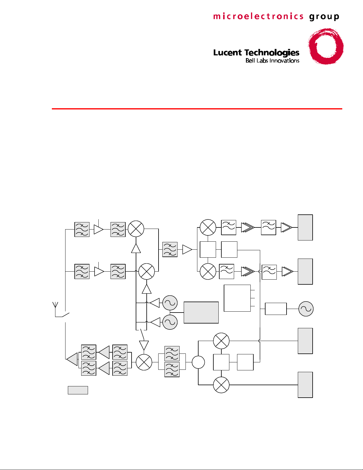
÷
Φ
W3000
FREQUENCY
SYNTHESIZER
2
RF MODE
& AGC
CONTROL
LO2 PLL
ADC
ADC
540 MHz VCO
DAC
RX I
RX Q
TX I
÷
2
÷
3
SWITCHED DIVIDER
DAC
TX Q
PA
GSM900
Note: shaded area is off-chip.
900: 270 MHz
Σ
Φ
Figure 1. W3020 Circuit Block Diagram
Page 2

Advance Data Sheet
W3020 GSM Multiband RF Transceiver December 1999
Table of Contents
Contents Page Contents Page
Features.................................................................1
Applications ...........................................................1
Description.............................................................4
Detailed Block Diagram......................................5
Pin Information.......................................................6
Absolute Maximum Ratings....................................8
ESD Precautions .................................................... 8
Operating Range .................................................... 8
Digital Serial Inputs................................................ 9
Digital Outputs .......................................................9
Enable Time...........................................................9
Supply Currents ..................................................... 9
LNA......................................................................10
RF Mixer.............................................................. 11
IF/Baseband Amplifier.......................................... 12
Modulator.............................................................15
LO2 Specification................................................. 17
List of Figures
Figure Page Figure Page
Figure 1. W3020 Circuit Block Diagram .................1
Figure 2. IC Block Diagram with Pinout.................. 5
Figure 3. IF Amplifier Gain Steps.........................12
Figure 4. Actual Gain vs. Requested Gain............ 12
Figure 5. IF Strip Balanced Input Matching
Network................................................ 12
Figure 6. IF Filtering Requirements for Wideband
Noise Performance................................16
LO1 Input Buffer Specification ..............................17
Programming Information.....................................18
Serial Bus Timing Information...........................19
The Data Word .................................................20
TR Register.......................................................21
CONFIG Register..............................................26
MAIN Register ..................................................30
Filter Tune and dc Offset Correction Timing......31
Programming Example .........................................33
Application Information .........................................35
S-Parameters....................................................35
Outline Diagram...................................................43
64-Pin TQFPT ..................................................43
Manufacturing Information ....................................44
Evaluation Board Note..........................................44
Ordering Information ............................................44
Figure 7. Diagram of W3020, W3000, and SC1
Interconnection...................................... 18
Figure 8. Serial Bus Timing Diagram....................19
Figure 9. IF and I/Q Gain Distribution (dB)............25
Figure 10. Programming the LO2 Phase Detector
Slope....................................................29
Figure 11. GSM900 Smith Chart Noise Circles.....35
Figure 12. GSM1800 Smith Chart Noise Circles... 36
2 Lucent Technologies Inc.
Page 3

Advance Data Sheet
December 1999 W3020 GSM Multiband RF Transceiver
List of Tables
Table Page Table Page
Table 1. Pin Assignment.........................................6
Table 2. GSM900 LNA Performance.....................10
Table 3. GSM1800/1900 LNA Performance.......... 10
Table 4. RF Performance: GSM900...................... 11
Table 5. RF Performance: GSM1800/1900...........11
Table 6. IF/Baseband Amplifier Performance .......13
Table 7. Low-Pass Rejection Characteristics.........14
Table 8. Modulator Performance...........................15
Table 9. LO2 Performance ...................................17
Table 10. LO1 Performance..................................17
Table 11. Serial Bus Timing Information............... 19
Table 12. Register Addressing..............................20
Table 13. TR Register........................................... 21
Table 14. B: Band Select......................................22
Table 15. MO[3:1]: Mode Control ..........................23
Table 16. T6: LO2 Disable.................................... 23
Table 17. T5: LO1 Disable.................................... 23
Table 18. T4: Receive IF Duty Cycle Corrector
Disable..................................................23
Table 19. T3: Divide-by-3 Duty Cycle Corrector
Disable..................................................23
Table 20. FTR: LPF Tune Filter Request .............. 24
Table 21. DP: dc Precharge Only .........................24
Table 22. DS: dc Correction Skip ..........................24
Table 23. T2: TX IF LO Division Select Switch .....24
Table 24. T1: TX IF LO Divide-by-6 Select ........... 24
Table 25. T0: TX IF Duty Cycle Corrector Disable.24
Table 26. G[0:6]: Digital Gain Control...................25
Table 27. CONFIG Register.................................. 26
Table 28. C10: LO2 PLL Enable ........................... 27
Table 29. OLD: Overload Output Disable.............. 27
Table 30. C9: RF Mixer On During Settling ...........27
Table 31. VO: LO1 Buffer Mode ...........................27
Table 32. C8: LO2 Charge Pump Off ....................27
Table 33. LD2: Lock Detect Enable....................... 28
Table 34. C7: dc Coarse/Fine Correction ............. 28
Table 35. C6: Filter Tune Disable......................... 28
Table 36. C5: dc Correction Disable ..................... 28
Table 37. C4: Low-Pass Filter Bandwidth............. 28
Table 38. C3: Receive LO1 Buffer Mode During dc
Calibration............................................ 29
Table 39. C2: LNA Mode During dc Calibration.... 29
Table 40. C1: 540 MHz LO2 Phase Detector
Polarity................................................. 29
Table 41. DT[2:0]: dc Correction Time ................. 30
Table 42. RS: Reset Bit Content .......................... 30
Table 43. Initialize CONFIG Register
(Reset W3020)..................................... 33
Table 44. Initialize TR Register............................ 33
Table 45. Settle PLL to GSM1800 Band for Receive
Mode (W3020/W3000)......................... 33
Table 46. Perform Receive (W3020).................... 34
Table 47. Settle PLL in GSM1800 Band for
Transmit Mode (W3020/W3000) .......... 34
Table 48. Basic GSM1800 Transmit Burst
(W3020)............................................... 34
Table 49. GSM900 LNA S-Parameters................. 37
Table 50. GSM1800/GSM1900 LNA
S-Parameters....................................... 38
Table 51. Receive IF Amplifier Input
(0 dB Setting)....................................... 39
Table 52. Receive IF Amplifier Input
(32 dB Setting)..................................... 39
Table 53. Transmit Modulator IF Output............... 40
Table 54. Transmit IF Input to Up-Conversion
Mixer .................................................... 41
Table 55. Transmit RF Output from Up-Conversion
Mixer .................................................... 42
Lucent Technologies Inc. 3
Page 4

Advance Data Sheet
W3020 GSM Multiband RF Transceiver December 1999
Description The W3020 is a highly integrated GSM transceiver
designed to operate in dual-band handsets or in
single-band handsets operating at 900, 1800, and
1900 MHz frequency bands (1900 MHz performance
is not verified in production). The IC architecture
allows the RF designer to provide solutions for three
different frequency bands with very few PCB changes,
thereby providing faster time to market and reduced
development time.
The W3020 RF transceiver and W3000 PLL have
been designed in conjunction with the SC1 (radio
interface and DSP) to provide a complete GSM
cellular solution. The W3020 interfaces to the W3000
UHF high-performance PLL IC. The W3020, in
combination with the W3000, provides the transmitter,
receiver, and frequency synthesizer. Adding a power
amplifier(s), filters, and VCO modules completes the
radio channel.
The baseband modulated signal is applied to the I/Q
double-balanced mixer in a differential manner. The
±45° phase-shifted local oscillator requires no trim to
achieve the required modulation spectral mask. Also,
I/Q input signals require no dc offset calibration to
achieve high phase accuracy signal. The IF signal
outputs from the I/Q mixers are summed and brought
out to an external filter that reduces the noise that
could be intermodulated into the receive band. This
signal is then applied to the low noise up-conversion
mixer and brought to the RF output.
The received signal is amplified through the low-noise
amplifier, which, combined with the preceding filter,
dominates the receiver sensitivity. The signal is then
passed through another external filter to attenuate the
image frequency to an acceptable level. The signal
passes through the RF down-conversion mixer to the
IF frequency. It is then filtered by an external surface
acoustic wave (SAW) filter to bring the in-band
blocking signals to an acceptable level. The signal is
amplified in the IF strip of the receiver. The IF strip
contains digital gain control (DGC) amplifiers at both
the IF and baseband frequencies and precision lowpass filters. This allows the signal to be amplified
while in-band blocking signals are removed. The
precision I/Q demodulator splits the signal into its inphase and quadrature signals. The I/Q signals are lowpass filtered and further amplified. The I/Q amplifier
contains integrated dc offset calibration circuitry. The
outputs (I/Q) are fed to the ADC for further signal
processing.
The second local oscillator (LO2), comprising a buffer
for the external voltage-controlled oscillator (VCO)
and a phase-locked loop (PLL), feeds the IF portions
of both the modulator and the receiver. An external
reference source, voltage-controlled crystal oscillator
(VCXO), is divided from 13 MHz to 1 MHz through a
counter. The 1 MHz is called the comparison
frequency. The VCO frequency of 540 MHz is also
divided down to 1 MHz. Both signals are fed into a
phase detector, and the resultant error signal is fed
through an external low-pass filter to the control input
of the VCO.
The RF receive and transmit mixers are driven by two
band-switchable external VCO modules and buffered
internally on the IC. The VCOs are both controlled by
a single W3000 PLL synthesizer and loop filter. Fast
band-locking is achieved using a proprietary scaling
technique integrated in the W3000 PLL.
4 Lucent Technologies Inc.
Page 5
Advance Data Sheet
December 1999 W3020 GSM Multiband RF Transceiver
Description (continued)
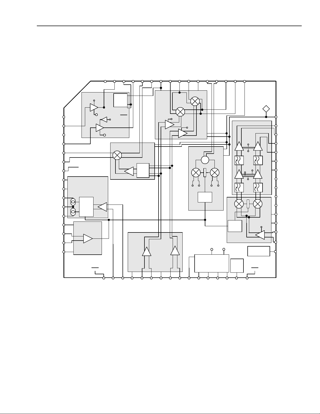
Detailed Block Diagram
EEL2
DLNAI
EEL3
GLNAI
TIFIP
TIFIN
GNDS4
GNDP2
VDDP2
VDDC2
CP2
GNDC2
VDDL2
L2P
L2N
GNDL2
R1
V
GND
TOUT
59
CC
DD
V
58
V
CCM
RF
MIXERS
V
DMIP
57
CCB
MIN
56
V
CCB
GMIP
EER1
54
55
EEGND
V
GND
MODULATOR
TIP TQNTQPTIN
CCB
∑
DIV BY
2 OR 3
TIFOP
53
TIFON
52
V
CC
GND
RMON
51
EEL1
DLNAO
GNDL
GLNAO
TOV
60
61
62
63
64
V
LNA
B
1800
1
2
3
LNA
900
EEL[1:3]
EEL[1:3]
CC
BIAS
GND
s
B
4
TX MIXER
5
6
GND
V
s
CC
7
8
9
MUX
10
11
LO2
PLL
12
13
V
14
15
16
GND
LO2
CC
BUFFER
540 MHz
GSM
1800
GSM
900
G[0:6]
B
DD
V
CONTROL LOGIC/
s s
V
CC
GND
SERIAL BUS
GND
RMOP
50
DIV BY
2
LO2
LOCK
R249
DD
V
4 dB
21 dB
G3
16 dB
4 dB
G1
G5
G6
G2
8 dB
G4
32 dB
TEST
V
GND
s
V
GND
CC
48
GNDS3
RIP
47
RIN
46
45
RQP
RQN
44
43
42
41
40
39
38
37
36
35
34
33
VDDB
GNDB
TQN
TQP
TIN
TIP
VDDI
GNDI
IFIP
IFIN
TEST
CC
32
31
30
29
28
27
26
25
24
23
22
21
20
19
18
17
GNDS1
MCI
MCG
L1
DD
V
DL1P
DL1N
GNDL1
GL1P
GL1N
DD
V
SS
V
CLK
DAT
LAT
LD
GNDS2
Figure 2. IC Block Diagram with Pinout
Lucent Technologies Inc. 5
Page 6

Advance Data Sheet
W3020 GSM Multiband RF Transceiver December 1999
Pin Information Table 1. Pin Assignment
Pin Symbol Type Pin Description
1 EEL2 Input* LNA Emitter Ground
2 DLNAI Input GSM1800/1900 Band LNA Signal Input
3 EEL3 Input* LNA Emitter Ground
4 GLNAI Input GSM900 Band LNA Signal Input
5 TIFIP Input TX IF Input to Mixer
6 TIFIN Input TX IF Input to Mixer
7 GNDS4 Ground Substrate Ground
8 GNDP2 Ground LO2 PLL Ground
9 VDDP2 Supply LO2 PLL Voltage Supply
10 VDDC2 Supply LO2 Charge Pump Supply
11 CP2 Output Charge Pump LO2 Output
12 GNDC2 Ground LO2 Charge Pump Ground
13 VDDL2 Supply LO2 Buffer Supply
14 L2P Input LO2 Positive Input (540 MHz)
15 L2N Input LO2 Negative Input (on-chip ac ground)
16 GNDL2 Ground LO2 Buffer Ground
17 GNDS1 Ground Substrate Ground
18 MCI Input Master Clock Input
19 MCG Input Master Clock Negative Input (ac ground)
20 VDDL1 Supply VDD Supply for LO1
21 DL1P Input GSM1800/1900 LO1 Positive Input
22 DL1N Input GSM1800/1900 LO1 Negative Input (on-chip ac ground)
23 GNDL1 Ground LO1 Ground
24 GL1P Input GSM900 LO1 Positive Input
25 GL1N Input GSM900 LO1 Negative Input (on-chip ac ground)
26 VDD Supply Voltage Supply for All Digital Circuits
27 VSS Ground Ground for All Digital Circuits
28 CLK Input Clock Input for Serial Bus
29 DAT Input Data Input for Serial Bus
30 LAT Input Latch Enable Input for Serial Bus
31 LD Output LO2 Synthesizer Lock Indicator Output
32 GNDS2 Ground Substrate Ground
*The emitters are considered critical inputs that need to be carefully grounded externally.
6 Lucent Technologies Inc.
Page 7

Advance Data Sheet
December 1999 W3020 GSM Multiband RF Transceiver
Pin Information (continued)
Table 1. Pin Assignment (continued)
Pin Symbol Type Pin Description
33 Test Output Production Test Output
34 IFIN Input IF DGC Amplifier Input Negative
35 IFIP Input IF DGC Amplifier Input Positive
36 GNDI Ground Ground for IF Amplifier
37 VDDI Supply Voltage Supply IF Amplifier
38 TIP Input TX In-Phase Positive Input
39 TIN Input TX In-Phase Negative Input
40 TQP Input TX Quadrature Positive Input
41 TQN Input TX Quadrature Negative Input
42 GNDB Ground Baseband RX Ground
43 VDDB Supply Baseband RX VDD Supply
44 RQN Output RX Quadrature Phase Negative Output
45 RQP Output RX Quadrature Phase Positive Output
46 RIN Output RX In-Phase Negative Output
47 RIP Output RX In-Phase Positive Output
48 GNDS3 Ground Substrate Ground RF dc Supply
49 VDDR2 Supply RF RX/TX Voltage Supply
50 RMOP Output RX Mixer Output Positive
51 RMON Output RX Mixer Output Negative
52 TIFON Output TX IF Output from Modulator Negative
53 TIFOP Output TX IF Output from Modulator Positive
54 EER1 Input* RX Mixer Emitter Ground
55 GMIP Input GSM900 Mixer Input Positive
56 MIN Input RF Mixer Input Negative (ac ground)
57 DMIP Input GSM1800 Mixer Input Positive
58 VDDR1 Supply RF RX Voltage Supply
59 TOUT Output Transmit Mixer Output
60 TOV Output Transmit Mixer Output
61 GLNAO Output GSM Band LNA Output
62 GNDL Ground LNA Substrate Ground
63 DLNAO Output GSM1800 Band LNA Output
64 EEL1 Input* LNA Emitter Ground
*The emitters are considered critical inputs that need to be carefully grounded externally.
Lucent Technologies Inc. 7
Page 8
Advance Data Sheet
W3020 GSM Multiband RF Transceiver December 1999
Absolute Maximum Ratings Stresses in excess of the absolute maximum ratings can cause permanent damage to the device. These are
absolute stress ratings only. Functional operation of the device is not implied at these or any other conditions in
excess of those given in the operations sections of this data sheet. Exposure to maximum ratings for extended
periods can adversely affect device reliability.
Parameter Symbol Min Max Unit
Ambient Operating Temperature TA –30 85 °C
Storage Temperature Tstg –65 150 °C
Lead Temperature (soldering, 10 s) — — 300 °C
Positive Supply Voltage VDD 0 4.5 V
Power Dissipation PD — 550 mW
ac Peak-to-Peak Input Voltage Vp-p 0 VDD V
Digital Voltages — 0 VDD V
ESD Precautions Although protection circuitry has been designed into this device, proper precautions should be taken to avoid
exposure to electrostatic discharge (ESD) during handling and mounting. Lucent Technologies Microelectronics
Group employs a human-body model (HBM) and a charged-device model (CDM) for ESD-susceptibility testing
and design evaluation. ESD voltage thresholds are dependent on the circuit parameters used to define the
model. No industry-wide standard has been adopted for CDM. However, a standard HBM (resistance = 1500 Ω,
capacitance = 100 pF) is widely used and, therefore, can be used for comparison purposes. The HBM ESD
threshold presented here was obtained by using these circuit parameters:
Parameter Method Rating Unit
ESD Threshold Voltage HBM 1500 V
ESD Threshold Voltage (corner pins) CDM 1000 V
ESD Threshold Voltage CDM 500 V
Operating Range The device is fully functional within the following operation ranges. No claims of parametric performance are
stated within this range. For parametric performance, refer to the individual specifications and operating
conditions.
Parameter Symbol Min Max Unit
Operating Temperature TA –30 85
Nominal Operating Voltage VDD 2.7 3.6 V
°C
8 Lucent Technologies Inc.
Page 9

Advance Data Sheet
December 1999 W3020 GSM Multiband RF Transceiver
Digital Serial Inputs
Parameter Symbol Min Max Unit
Logic High Voltage VIH 0.7 * VDD — V
Logic Low Voltage VIL — 0.3 * VDD V
Logic High Current (VIH = 3.0 V) |IIH| — 10
Logic Low Current (VIL = 0.0 V) |IIL| — 10
µA
µA
Clock Input Frequency (VDD = 2.7 V) fCLK — 10 MHz
Digital Outputs
Parameter Symbol Min Max Unit
Logic High Voltage VOH VDD – 0.4 — V
Logic Low Voltage VOL — 0.4 V
Logic High Current (VOH ≥ VDD –
|IOH| 2 — mA
0.4)
Logic Low Current (VOL ≤ 0.4 V)
|IOL| 2 — mA
Enable Time VDD = 2.7 Vdc; TA = 25 °C ± 3 °C.
Parameter Min Typ Max Unit
Logic Powerup/down Time — — 4.0
µs
Supply Currents VDD = 2.7 Vdc; TA = 25 °C ± 3 °C.
System Mode Min Typ Max Unit
Powerdown (VDD = 3.0
— 2 50
µA
Vdc)*
PLL RX Settling — 33 — mA
RX Mode (LNA = ON) — 68 — mA
RX Mode (LNA = OFF) — 64 — mA
PLL TX Settling — 33 — mA
TX Mode — 92 — mA
*This current does not include LO2 charge pump supply current. (See LO2 specification for details.)
Lucent Technologies Inc. 9
Page 10

Advance Data Sheet
W3020 GSM Multiband RF Transceiver December 1999
LNA
The W3020 contains two on-chip LNAs, one to operate in the GSM900 band and one to operate in the
GSM1800/1900 bands. The GSM900 operation is combined with the GSM1800 band operation in a dual-band
terminal. Only one LNA operates at a time. The two on-chip LNAs with external matching networks are 50 Ω
single-ended input, single-ended output type. Switching between the LNAs is determined by the band bit B and
the gain control bit G0 in the TR register, as described in the Programming Information section.
Table 2. GSM900 LNA Performance VDD = 2.7 Vdc; TA = 25 °C ± 3 °C.
Parameter Min Typ Max Unit
RF Input Band 925 — 960 MHz
Current Consumption (collector current) — 3.5 — mA
Noise Figure* — 2.0 — dB
Power Gain (942 MHz)* — 20 — dB
Input 1 dB Compression Level –20 –15 — dBm
Input Return Loss — 14 — dB
Off-state Gain — –51 — dB
* All gain and NF include matching losses. Not tested in production. Table 3. GSM1800/1900 LNA Performance
VDD = 2.7 Vdc; TA = 25 °C ± 3 °C.
Parameter Min Typ Max Unit
RF Input Band:
GSM1800 1805 — 1880 MHz
GSM1900 1930 — 1990 MHz
Current Consumption (collector current) — 3.5 — mA
Noise Figure* — 3.0 — dB
Power Gain (1842 MHz)* — 19 — dB
Input 1 dB Compression Level –20 –16.5 — dBm
Input Return Loss — 15 — dB
Off-state Gain — –38 — dB
* All gain and NF include matching losses. Not tested production.
10 Lucent Technologies Inc.
Page 11
Advance Data Sheet
December 1999 W3020 GSM Multiband RF Transceiver
RF Mixer The W3020 contains two mixers: one for GSM900 band operation and one for GSM1800/1900 band operation.
The RF mixers are double-balanced mixers that can be used in various modes of operation. The ac-grounded
input (pin 56) requires grounding at both the RF and the IF frequencies. If grounding is not placed close to the
device, the RF performance will be compromised. At the output, the mixer is connected to a balanced IF SAW
filter.
Table 4. RF Performance: GSM900 VDD = 2.7 V; TA = 25 °C ± 3 °C. FIN = 942 MHz
Parameter Min Typ Max Unit
RF Input Band 925 — 960 MHz
Output IF Frequency — 270 — MHz
LO Frequency Range 1195 — 1230 MHz
Noise Figure (SSB) — 9 12 dB
Mixer Power Gain* 7 dB
I/P 1 dB Compression –10 –5 — dBm
*LO1 level = –6 dBm, FLO = 1212 MHz, FIF= 270 MHz.
Table 5. RF Performance: GSM1800/1900 VDD = 2.7 V; TA = 25 °C ± 3 °C. FIN = 1842 MHz
Parameter Min Typ Max Unit
RF Input Band:
GSM1800 1805 — 1880 MHz
GSM1900 1930 — 1990 MHz
Output IF Frequency — 270 — MHz
LO Frequency Range:
GSM1800 1535 — 1610 MHz
GSM1900 1660 — 1720 MHz
Noise Figure (SSB) — 9.5 12 dB
Mixer Power Gain* 4 6 — dB
I/P 1 dB Compression –12 –7 — dBm
*LO1 level = –6 dBm, FLO = 1572 MHz, FIF = 270 MHz
Lucent Technologies Inc. 11
Page 12
Advance Data Sheet
W3020 GSM Multiband RF Transceiver December 1999
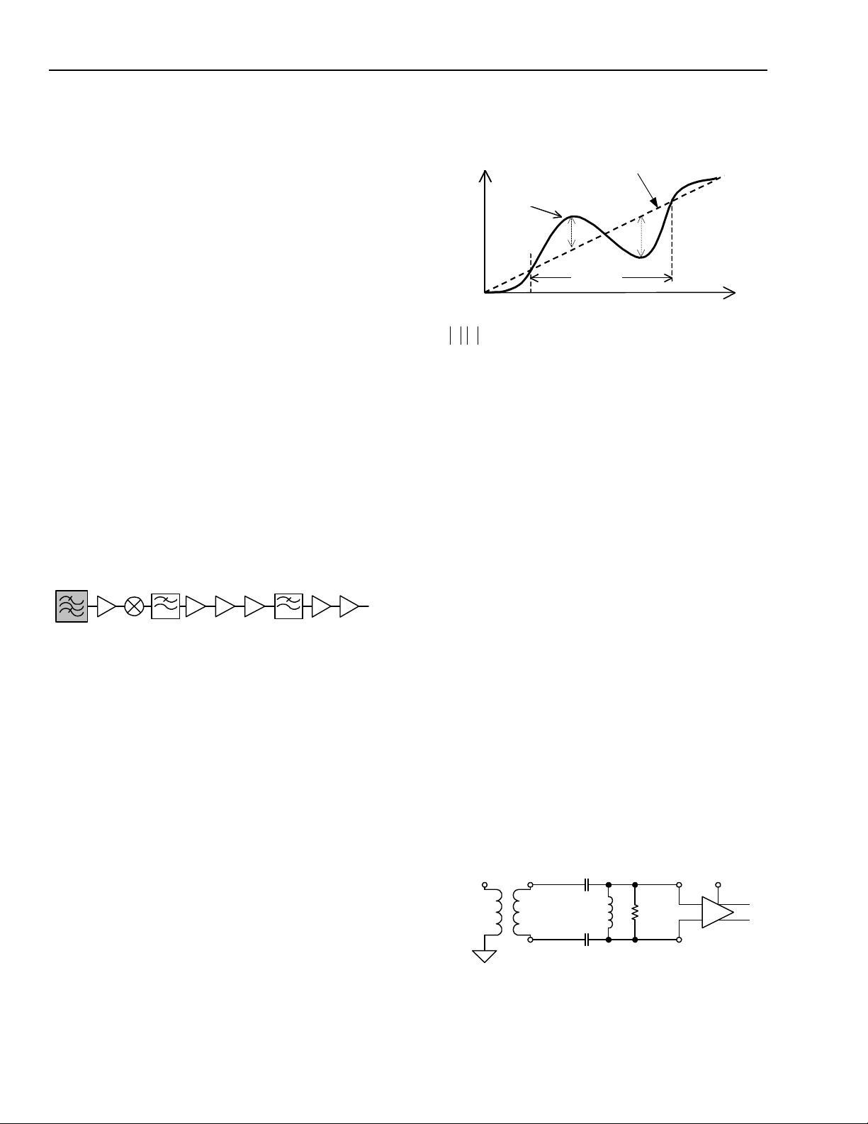
IF/Baseband Amplifier The IF amplifier is a balanced-input/balanced-output
type and is connected to a balanced SAW filter. It
consists of three gain stages: an IF amplifier and two
sections of baseband amplifiers. The gain can be
changed in steps of 32, 16, 8, and 4 dB. The baseband also contains a level-shifter stage to drive an
A/D converter directly. The level-shifter stage has 21
dB of gain that can be switched off. The specifications
below are for the two modes of operation.
The gain of the IF section is programmed via the
three-wire serial bus.
The IF amplifier contains the 32 dB amplifier stage
and has a gain of either 0 or 32 dB. The IF amplifier is
followed by a quadrature mixer with a fixed gain of
4 dB. The first baseband amplifier (G3, G2, G6) after
the low-pass filter and demodulator has gains
selectable between 0, 4, 8, 12, 16, 20, 24, and 28 dB.
Using the other gain steps, the IF and baseband gain
can be varied by 64 dB in 4 dB steps. The second
baseband amplifier (G5, G1) has gains selectable
between 0, 4, 21, and 25 dB. The 21 dB gain step in
the second baseband amplifier section is not tested
and should therefore not be used. Figure 3 is a
diagram of the gain steps.
gain accuracy is determined after calibration of the
32 dB amplifier.
ACTUAL
GAIN (dB)
ACTUAL GAIN
ACTUAL = REQUESTED
X
20 dB
Y
REQUESTED GAIN (dB)
Note: =Y,X relative gain accuracy.
Figure 4. Actual Gain vs. Requested Gain
The input impedance of the IF strip will vary slightly
when the 32 dB amplifier is switched between the ON
and OFF states. We recommend that the IF strip be
matched with the 32 dB amplifier in the ON state to
provide the best match to the SAW filter when the
input level is at a minimum. The input matching
network can match the IF input directly to the SAW
filter or to 50 Ω.
G4
32/0
*Not tested.
6
G3 G2 G6* G1G5*LPF1 LPF2
16/0
8/0
4/0
21/0
4/0
Figure 3. IF Amplifier Gain Steps
The baseband amplifier section contains dc correction
circuitry that minimizes dc offsets at the I/Q outputs.
The low-pass filters in the baseband contain a selfcalibrating circuit for tuning of filter cut-off frequency.
The selectable gain settings are programmed via the
TR register as described in the Programming
Information section. Filter tuning and dc calibration
are also explained in that section.
To achieve the specified absolute gain accuracy, the
total gain should be calibrated at room temperature.
This would normally be part of the overall phone
calibration. Absolute gain accuracy measures the gain
change over a specified temperature range relative to
the room temperature measurement. In the GSM
system, this specification is dependent on all the RX
functional blocks and not solely on the IF strip. The
relative gain accuracy is a measure of the gain stage
accuracy over a 20 dB range (see Figure 4). Relative
A matching network to 50 Ω was chosen for the
evaluation board to allow for convenient laboratory
measurements. To keep the input impedance low and
minimize impedance variation between gain settings
of the IF stage, a resistor is shunt-connected between
the input terminals. The input network can then be
matched to the desired input impedance. (The
specified gain includes a resistor value of 500 Ω.) For
testing purposes, the input has been matched to 50 Ω,
and the gains of the IF/baseband amplifier are all
referred to a 50 Ω matched input impedance. The I/Q
outputs are terminated in high-impedance loads. The
gains are voltage gains and include the voltage gain in
the impedance transformation of the input matching
network. The network is illustrated in Figure 5.
W3020 G4 bit
IFIP PIN 35
INPUT
IMPEDANCE
50
Ω
1:1
Note: Balun is shown for testing purposes only.
R1
500
Ω
IFIN PIN 34
32/0
Figure 5. IF Strip Balanced Input Matching
Network
12 Lucent Technologies Inc.
Page 13

Advance Data Sheet
December 1999 W3020 GSM Multiband RF Transceiver
IF/Baseband Amplifier (continued) Table 6. IF/Baseband Amplifier Performance
VDD = 2.7 V; TA = 25 °C ± 3 °C.
Parameter Min Typ Max Unit
Total Voltage Gain (referred to 50 Ω input)*
60 65 68 dB
Demodulator Gain — 4 — dB
Absolute Gain Accuracy
Relative Gain Step Accuracy
Noise Figure (matched to 50 Ω)
†
‡
§
O/P 1 dB Compression Point (0 dB gain
–2.0 — 2.0 dB
–1.0 — 1.0 dB
— 6.2 12 dB
— –1.5 — dBm(V)**
setting)
O/P 1 dB Compression Point (>16 dB
12 — — dBm(V)**
baseband gain setting)
Output Load Capacitance (differential)
Output Load Capacitance (single-end to
— — 10 pF
— — 10 pF
ground)
Output Load Resistance (differential)
Output Load Resistance (single-end to
20 — —
40 — —
kΩ
kΩ
ground)
IF Enable Time — — — µs
I/Q Common-mode Output Voltage 0.5 * VDDB – 0.15 0.5 * VDDB 0.5 * VDDB + 0.15 V
I/Q Output Current
I/Q Phase Accuracy
I/Q Amplitude Mismatch
I/Q Differential Offset Voltage
(corrected)
§,††
Offset Correction Decay Rate
§
§
§
IF Input Impedance (diffferential)
32 dB gain setting
0 dB gain setting
* 64 dB DGC setting. This voltage gain is measured from the input of the IF strip to either the I or Q channel output.
±50
— 3.5 — degrees
–1 ±0.1 1 dB
— 5 ±50 mV
— 2 — mV/s
—
—
— — µA
114 – j497
92 – j497
—
—
Ω
Ω
† The absolute accuracy refers to the total gain variation from the nominal condition over temperature (–30 °C to +85 °C) after gain calibration at
nominal temperature.
‡ The relative gain step accuracy is determined after the 32 dB gain stage has been calibrated at nominal temperature. The total gain step accuracy
at any of the possible gain conditions should not vary more than the specified amount within a 20 dB measurement window.
§ At 64 dB gain setting.
** This is a voltage and specified in dBm as if the voltage were across a 50 Ω load.
††Offset tested in coarse dc-correction mode only.
Lucent Technologies Inc. 13
Page 14

Advance Data Sheet
W3020 GSM Multiband RF Transceiver December 1999
IF/Baseband Amplifier (continued) Table 7. Low-Pass Rejection Characteristics
VDD = 2.7 V; TA = 25 °C ± 3 °C; high bandwidth.
Parameter Min Typ Max Unit
Corner Frequency* 130 168 226 kHz
Group Delay Distortion (0 kHz—75 kHz) — 61 — ns
Attenuation:
75 kHz — 0.4 — dB
100 kHz — 0.8 — dB
200 kHz — 4.7 — dB
400 kHz — 18 — dB
600 kHz — 28 — dB
800 kHz — 35 — dB
1.6 MHz — 53 — dB
3.0 MHz — 69 — dB
* After filter tuning. (See FilterTune and dc Offset Correction Tuning section.)
14 Lucent Technologies Inc.
Page 15

Advance Data Sheet
December 1999 W3020 GSM Multiband RF Transceiver
Modulator The modulator uses an indirect I/Q modulator architecture that is ideal for multiband operation. The IF
modulation improves EVM effects due to improved carrier feedthrough. The series transmit IF filters allow
improved wideband noise, which enables duplexer removal. The I/Q modulator requires no amplitude or phase
calibration to achieve high phase accuracy. The modulator can be altered between GSM900 transmit mode (TX
IF = 270 MHz) and GSM1800/1900 transmit mode (TX IF = 180 MHz) by the band bit setting in the TR register.
Table 8. Modulator Performance VDD = 2.7 V; TA = 25 °C ± 3 °C. IQ common mode = 1.6 V; input differential signal = 1.0 Vp-p.
Parameter Min Typ Max Unit
I/Q Signal Path Bandwidth — 450 — kHz
I/Q Input Resistance to Ground 25 — —
kΩ
I/Q Input Capacitance to Ground — — 10 pF
I/Q Input Resistance (differential) 10 — —
kΩ
I/Q Input Capacitance (differential) — — 10 pF
I/Q Common-mode Range 1.5 — VDD – 1.05 V
I/Q Input Differential Signal for Max Output 0.8 1 1.2 Vp-p
RF Output Band:
GSM900
GSM1800
GSM1900
Output Power:
GSM900 (LO1 at 1167 MHz)
GSM1800 (LO1 at 1567 MHz)
Powerup Time* — — 4
RMS Phase Accuracy
†:
GSM900
GSM1800
880
1710
1850
–4.5
–4
—
—
—
—
—
0
0
2.0
2.5
915
1785
1910
6
6
MHz
MHz
MHz
dBm
dBm
µs
—
—
°rms
°rms
GMSK Modulation Spectrum (max) (offset from carrier):
100 kHz @30 kHz RBW — — 0.5 dBc
200 kHz — — –30 dBc
250 kHz — — –33 dBc
400 kHz — — –60 dBc
1.8 MHz—3.0 MHz @100 kHz RBW — — –65 dBc
3.0 MHz—6.0 MHz — — –65 dBc
>6.0 MHz — — –73 dBc
Wideband Noise IF Modulator
GSM900:
|f – f0| ≥ 10 MHz
|f – f0| ≥ 20 MHz (PM)
— –140 — dBc/Hz
— –140 — dBc/Hz
GSM1800:
|f – f0| ≥ 20 MHz (PM)
— –140 — dBc/Hz
Wideband Noise RF Mixer (See Figure 6.):
GSM900:
|f – f0| ≥ 10 MHz
|f – f0| ≥ 20 MHz (PM)
— –154 — dBc/Hz
— –154 — dBc/Hz
GSM1800:
|f – f0| ≥ 20 MHz (PM)
— –153 — dBc/Hz
* From the programming latch going high to power available at RF output, Including TX IF filter group delay.
† Including contributions from LO1, LO2, and modulator.
Lucent Technologies Inc. 15
Page 16

Advance Data Sheet
W3020 GSM Multiband RF Transceiver December 1999
Modulator (continued)
I
LO2
÷2
÷3
Q
Φ
REJECTION = 34 dB @ 20 MHz OFFSET
IL = 3 dB
LO1
OUTPUT
Figure 6. IF Filtering Requirements for Wideband Noise Performance
16 Lucent Technologies Inc.
Page 17

Advance Data Sheet
December 1999 W3020 GSM Multiband RF Transceiver
LO2 Specification The W3020 contains an input buffer for an external VCO and a PLL for generation of a second LO signal at
540 MHz. The output of the buffer is fed to the receive and transmit circuits, where the signal is divided to the IF
frequency. The phase noise includes contributions from VCO buffers to the transmit and receive circuits.
Table 9. LO2 Performance VDD = 2.7 V; TA = 25 °C ± 3 °C.
Parameter Min Typ Max Unit
Charge Pump Supply (VDDC2) 2.7 2.85 3.0 V
Frequency — 540 — MHz
LO2 Input Level –6 –3 0 dBm
Clock Reference Frequency — 13.0 — MHz
Clock Input Level 0.4 1 — Vp-p
Reference Frequency (at phase detector) — 1.0 — MHz
Phase Accuracy (loop bandwidth 10 kHz) — 1.3 —
Phase Detector Gain (VDD = 2.85 V) — 200 —
Powerdown Charge Pump Supply Current (VDDC2) — — 1 mA
Phase Detector Voltage 0.5 1.3 VDDC2 – 0.5 V
°rms
µA/cycle
Note: Reference sidebands determined by external loop filter components.
LO1 Input Buffer Specification Table 10. LO1 Performance
VDD = 2.7 V; TA = 25 °C ± 3 °C.
Parameter Min Typ Max Unit
Frequency Range:
GSM900 1150 — 1230 MHz
GSM1800 1530 — 1610 MHz
GSM1900 1660 — 1730 MHz
Input Power Level –6 –3 — dBm
Input Noise Figure — 8 10 dB
Lucent Technologies Inc. 17
Page 18

Advance Data Sheet
W3020 GSM Multiband RF Transceiver December 1999
Programming Information The W3020 and W3000 transceiver mode (IC RX/TX) and the gain and band settings are programmed using a
standard three-wire bus (CLOCK, DATA, LATCH). The W3020 and W3000 registers are addressable so the two
ICs can share the same data, clock, and latch times. The LATCH line initiates download and execution of the
current DATA word.
TR REGISTER
CONFIG REGISTER
MAIN REGISTER
W3020
W3000
MAIN REGISTER
REF REGISTER
PARALLEL LATCH SERLE1
SERIAL SHIFT
SERIAL SHIFT
PARALLEL LATCH
ADDRESS
ADDRESS DECODER
A[0:2]
LAT
CLK
DAT
DAT
CLK
LAT
A[0:2]
DECODER
Figure 7. Diagram of W3020, W3000, and SC1 Interconnection
SC1
SERCK
SERDA
18 Lucent Technologies Inc.
Page 19

Advance Data Sheet
December 1999 W3020 GSM Multiband RF Transceiver
Programming Information (continued) Serial Bus Timing Information
DAT
LSB
CLK
MSB
CS
t
MSB – 1
CH
t
LAT
LAT
OR
L
t
L
V
t
CWL
t
CWH
t
Figure 8. Serial Bus Timing Diagram
Table 11. Serial Bus Timing Information VDD = 2.7 V; TA = 25 °C ± 3 °C
Symbol Parameter Min Typ Max Unit
TCS Data to Clock Setup Time 33 — — ns
TCH Data to Clock Hold Time 10 — — ns
TCWH Clock Pulse Width High 33 — — ns
TCWL Clock Pulse Width Low 33 — — ns
TLS Clock Falling Edge to Latch High Setup Time 0 — — ns
TLWH Latch Pulse Width 50 — — ns
TLL Latch to Clock Setup Time 33 — — ns
FCLK Clock Input Frequency — — 10 MHz
LS
t
LWH
t
Lucent Technologies Inc. 19
Page 20

Advance Data Sheet
W3020 GSM Multiband RF Transceiver December 1999
Programming Information (continued) The Data Word The W3020 and W3000 chips are addressed through the bit content of the 24-bit serial word. Some words for
time-critical interactions address both W3020 and W3000 at the same time, while some words for initialization
address W3020 and W3000 separately.
The W3020 gets all of its control information via a three-wire serial bus from the baseband IC. Serial data
transfers always consist of 24 bits: 3 bits of address to select one of five control registers, and up to 21 bits of
data. The data is shifted first into a shift register and then parallel-loaded into the proper control register after the
completion of the transfer when the latch enable signal goes high. The last bit is that which immediately precedes
a low-to-high latch input transition occurring while the CLOCK input is low. Bit 24 is loaded first, and bit 1 is
loaded last. The four control registers are defined as follows:
n TR: Transmit/receive register for W3020. Contains bits for setting various transmit and receive modes, setting
receive gain, etc. It is expected that this register would be written several times during a frame.
n CONFIG: Contains bits to control various options for dc offset correction, filter-tuning, lock detect, and
overload outputs, etc. It is expected that this register would be written once at initialization and then rarely
updated. Since it is not affected by the power-on reset circuit, a write to this register should be the first
operation performed when accessing the W3020 chip. Also, it is advisable never to update the configuration
register while a critical operation is in progress.
n MAIN: Main counter and prescaler values for W3000 chip. Used to set mode and band bit functions for the
W3020 while programming the W3000.
n REF: Reference counter values for W3000. Not relevant to W3020.
Table 12. Register Addressing
A2 A1 A0 Register Device
1 0 0 TR W3020
1 0 1 CONFIG W3020
1 1 0 RESERVED W3020
1 1 1 RESERVED W3020
0 X 0 M MAIN W3000
0 X 1 M REF W3000
Note: X indicates that the bit does not affect addressing for the given
combination of A2 and A0 that addresses the W3000. In the W3000, the
A1 bit is used for data content.
20 Lucent Technologies Inc.
Page 21

Advance Data Sheet
December 1999 W3020 GSM Multiband RF Transceiver
Programming Information (continued) TR Register The TR register is the transmit/receive register for W3020. It contains bits for setting various transmit and
receive modes, setting receive gain, etc. It is expected that this register would be written several times during a
frame.
Last bit in serial sequence First bit in serial sequence
Bit No. 1 2 3 4 5 6 7 8 9 10 11 12 13 14 15 16 17 18 19 20 21 22 23 24
A0=0 A1=0 G0 G1 G2 G3 G4 G5 G6 T0 T1 T2 DS DP FTR T3 T4 T5 T6 MO1 MO2 MO3 B A2=1
Bit
Table 13. TR Register
Bit Number Bit SC1 Standard
Function
Setting
24 A2 1 Address Bit
23 B 0 Band Select (See Table 14.)
22
21
20
MO3
MO2
MO1
— RX, TX, Synthesizer Mode (See Table 15.)
19 T6 0 Disable LO2 Circuitry in All Modes (See Table 16.)
18 T5 0 Disable LO1 Circuitry (W3000 excluded) (See Table 17.)
17 T4 0 RX IF Duty Cycle Corrector Disable (See Table 18.)
16 T3 0 GSM1800 TX IF LO Divide-by-3 Duty Cycle Corrector Disable (See
Table 19.)
15 FTR 1 LPF Tune Filter Request (See Table 20.)
14 DP 0 dc Precharge Only (See Table 21.)
13 DS 0 dc Correction Skip (See Table 22.)
12 T2 0 LO2 Divide by 2 or Divide-by-3 Select for TX IF (See Table 23.)
11 T1 0 TX IF LO Divide-by-6 Select (See Table 24.)
10 T0 0 TX IF Duty-Cycle Corrector Disable (See Table 25.)
9
8
7
6
5
4
G6
G5
G4
G3
G2
G1
— Digital Gain Control RX IF/IQ-Baseband (See Table 26.)
3 G0 1 Digital Gain Control LNA On/Off (See Table 26.)
2
1
A1
A0
0
Address Bits
0
Note: The TR register is reset to an all-zero state after the reset bit in the CONFIG register has been set high.
Lucent Technologies Inc. 21
Page 22

Advance Data Sheet
W3020 GSM Multiband RF Transceiver December 1999
Programming Information (continued)
TR Register (continued)
B: Band Select
When set low, the GSM900 transceiver circuits are
enabled and the GSM1800 transceiver circuits are
disabled. When set high, the GSM1800 transceiver
circuits are enabled and the GSM900 transceiver
circuits are disabled. The transceiver circuits that
change with the setting of the band bit B are the LNA,
the RF mixer, the receive UHF LO1 buffer, the
transmit UHF LO1 buffer, and the LO2 divider for the
modulator IF LO phase shifter circuit. The normal LO2
division factor for GSM900 is divide-by-2; for
GSM1800, the normal LO2 division factor is divide-by-
3. Note that bits T2 and T1 also affect the transmitter
LO2 division factor when set high (see Table 23 and
Table 24).
Table 14. B: Band Select
B
Function
Bit 23
0 GSM900 Path On
1 GSM1800/1900 Path On
Note: When programmed via the same three-wire bus as
the W3000, updating this bit in W3020 also
updates it in W3000, and vice versa.
MO[3:1]: Mode Control
The various system modes of the W3020 are set by
the mode control bits. These are active in both the TR
and MAIN registers. The W3000 will also power up
with the W3020 in any of the valid modes set by the
mode bits in the TR or MAIN registers. The mode bit
settings for each W3020 system mode are given in
Table 15. The corresponding typical supply current for
the IC in each mode is shown in the Supply Currents
table on page 9.
In sleep mode, both the W3020 and W3000 are
powered down, and the supply current is in the µA
range. The transmit PLL settling mode is used prior to
a transmit burst in order to power up and lock the LO1
and LO2 VCO/PLL synthesizers and the respective
RF and IF LO buffers connecting to the modulator
circuit. The LO2 divide-by circuits remain off during
this mode. Similarly, the receive PLL settling mode is
used prior to the receive dc calibration time slot and
subsequent receive burst in order to power up and
lock the LO1 and LO2 VCO/PLL synthesizers and the
respective RF and IF LO buffers connecting to the RF
mixer and IF strip. The RF mixer can be turned on in
this mode by setting the C9 (RF mixer on during
settling) bit high in the CONFIG register (see Table
30). The transmitter ON mode turns on all the same
circuits as the transmit PLL settling mode along with
the I/Q modulator and up-conversion mixer.
The receiver ON mode turns on all the same circuits
as the receive PLL settling mode along, with the LNA
(if enabled by the G0 bit—see Table 26), RF mixer,
and IF amplifiers and demodulator. When first going
into receive mode, a baseband LP filter tune is
performed, if requested, by setting the FTR (filter tune
request) bit high in the TR register and the C6 (filter
tune disable) bit low in the CONFIG register (see
Table 20 and Table 35, respectively, and the LowPass Filter Tuning section). Next, a dc offset
calibration cycle is performed if the DS (dc correction
skip) bit is low in the TR register and the C5 (dc
correction disable) bit is low in the CONFIG register
(see Table 22 and Table 36, respectively). The default
condition is that the LNA turns off during the dc
calibration if the C2 (LNA mode during dc calibration)
bit is low in the CONFIG register (see Table 37). The
other default condition is that the RF mixer LO1 buffer
turns off during the dc calibration if the C3 (RX LO1
buffer mode during dc calibration) bit is low in the
CONFIG register (see Table 38).
During this event, the transmit LO1 buffer will turn on
to act as a load stage for the UHF LO1 buffer. (For
additional information on the dc offset calibration, see
the dc Offset Correction Timing section.) After the dc
calibration cycle, all the receive circuits turn on as
mentioned above for the receive burst.
22 Lucent Technologies Inc.
Page 23

Advance Data Sheet
December 1999 W3020 GSM Multiband RF Transceiver
Programming Information (continued) TR Register (continued) Table 15. MO[3:1]: Mode Control
MO3 MO2 MO1 Function
Bit 22 Bit 21 Bit 20
0 0 0 Sleep: All Modules Powerdown
0 0 1 Reserved
0 1 0 Reserved
0 1 1 Reserved
1 0 0 TX PLL Settling Mode (LO1, LO2, TX LO1, and TX LO2 buffers on)
1 0 1 RX PLL Settling Mode (LO1, LO2, RX LO1, and RX LO2 buffers on)
1 1 0 TX ON (TX modulator and mixer, LO1, LO2, TX LO1, and TX LO2 buffers on)
1 1 1 RX ON (RX mixer; LNA, if enabled; IF amplifier; LO1; LO2; RX LO1; and RX LO2
buffers on)*
*If MO bits are set to 111 with the dc correction skip bit low, a dc offset calibration cycle is performed automatically. Table 16. T6: LO2 Disable
If this bit is set high, the 540 MHz LO2 input buffer
and LO2 PLL will be turned off. This bit will also
disable the 13 MHz clock buffer going to the
baseband amplifier correction circuits. This bit is
provided for testing purposes.
T6
Bit 19
0 LO2 Circuit Enabled
1 LO2 Circuit Disabled
Table 17. T5: LO1 Disable The T5 bit disables the LO1 circuitry including the
UHF LO1 buffer and bias circuit. This bit is provided
for testing purposes.
T5
Bit 18
0 LO1 Circuitry Enabled
1 LO1 Circuitry Disabled
Function
Function
Table 18. T4: Receive IF Duty Cycle Corrector
Disable
When high, disables duty cycle correction circuit in
the LO2 divide-by-2 circuit for the receive IF
demodulator. This is provided for testing purposes.
T4
Bit 17
0 Divide-by-2 Duty Cycle Corrector Enabled
1 Divide-by-2 Duty Cycle Corrector Disabled
Table 19. T3: Divide-by-3 Duty Cycle Corrector
Disable
When high, disables duty cycle correction circuit in
the GSM1800/1900 transmit IF LO divide-by-3
circuit. This is provided for testing purposes.
T3
Bit 16
0 Divide-by-3 Duty Cycle Corrector Enabled
1 Divide-by-3 Duty Cycle Corrector Disabled
Function
Function
Lucent Technologies Inc. 23
Page 24

Advance Data Sheet
W3020 GSM Multiband RF Transceiver December 1999
Programming Information (continued) TR Register (continued) Table 20. FTR: LPF Tune Filter Request
This requests tuning operation of baseband low-pass
filter (see the Low-Pass Filter Tuning section for
details). If the filter tune is enabled in CONFIG
register, the FTR bit must be programmed high before
the first following receive mode is active. Filter tune
can only be done in a mode where LO2 is active, e.g.,
receive mode.
FTR
Bit 15
0 Use Default Tuning Value
1 Perform New Tuning
Table 21. DP: dc Precharge Only When dc offset calibration is performed, only the
precharge portion is done. This reduces the amount of
time required for dc offset calibration, but gives higher
levels of dc offset. (See the dc Offset Calibration
section for details.)
DP
Bit 14
0 Standard dc Offset Correction Cycle
1 dc Precharge Cycle Only
Table 22. DS: dc Correction Skip
DS
Bit 13
0 Insert dc Correction Cycle (See Table
41.)
1 Skip dc Offset Calibration (with retained
dc correction setting)
Function
Function
Function
Table 23. T2: TX IF LO Division Select Switch Reverses the LO2 frequency division factor in the
transmitter for both bands. This is provided for testing
purposes. This bit works with the band bit B as follows.
T2
Bit 12 BBit 23
0 0 Divide by 2 (270 MHz):
Normal GSM900 Division
0 1 Divide by 3 (180 MHz): Normal
GSM1800/1900 Division
1 0 Divide by 3 (180 MHz): Reversed
Band 0 Division
1 1 Divide by 2 (270 MHz): Reversed
Band 1 Division
Table 24. T1: TX IF LO Divide-by-6 Select This bit will change the divide-by-3 circuit to a divide-
by-6 circuit. This bit is provided for testing purposes.
T1
Bit 11
0 Divide by 3 when 1/3 Path Is Active
1 Divide by 6 when 1/3 Path Is Active
Table 25. T0: TX IF Duty Cycle Corrector Disable When high, disables duty cycle correction circuit into
the transmit IF phase splitter. This bit is provided for
testing purposes.
T0
Bit 10
0 TX IF LO Duty Cycle Corrector Enabled
1 TX IF LO Duty Cycle Corrector Disabled
Function
Function
Function
24 Lucent Technologies Inc.
Page 25

Advance Data Sheet
December 1999 W3020 GSM Multiband RF Transceiver
Programming Information (continued) TR Register (continued) Table 26. G[0:6]: Digital Gain Control
Digital RX gain control with bits defined as follows:
G0: When high, enables GSM900 or GSM1800/1900 LNA according to which band is selected by band bit B.
(See Table 14.)
G4: IF gain: 0 = 0 dB, 1 = 32 dB.
G1: 0 = add 0 dB to baseband gain, 1 = add 4 dB to baseband gain in second amplifier.
G2: 0 = add 0 dB to baseband gain, 1 = add 8 dB to baseband gain in first amplifier.
G3: 0 = add 0 dB to baseband gain, 1 = add 16 dB to baseband gain in first amplifier.
G5: 0 = add 0 dB to baseband gain, 1 = add 21 dB to baseband gain in second amplifier.
G6: 0 = add 0 dB to baseband gain, 1 = add 4 dB to baseband gain in first amplifier.
The nominal demodulator mixer conversion gain is 4 dB; hence, total gain is always 4 dB higher than the DGC setting.
Voltage gain is differential assuming input matching network to 50 Ω source impedance. (See Table 6.)
G6 G5 G4 G3 G2 G1 DGC Gain Total Gain
Bit 9 Bit 8 Bit 7 Bit 6 Bit 5 Bit 4 (dB) (dB)
0 0 0 0 0 0 0 4
1 0 0 0 0 0 4 8
0 0 0 0 1 0 8 12
1 0 0 0 1 0 12 16
0 0 0 1 0 0 16 20
1 0 0 1 0 0 20 24
0 0 0 1 1 0 24 28
1 0 0 1 1 0 28 32
0 0 1 0 0 0 32 36
1 0 1 0 0 0 36 40
0 0 1 0 1 0 40 44
1 0 1 0 1 0 44 48
0 0 1 1 0 0 48 52
1 0 1 1 0 0 52 56
0 0 1 1 1 0 56 60
1 0 1 1 1 0 60 64
1 0 1 1 1 1 64 68
0 1 0 0 0 0 21 25*
1 1 1 1 1 0 81 85*
1 1 1 1 1 1 85 89*
* Not tested or recommended for use.
G4 G3 G2 G6* G5* G1LPF1 LPF2
6
16/0 8/0 4/0 21/0
4/0
*Not tested.
32/0
Figure 9. IF and I/Q Gain Distribution (dB)
Lucent Technologies Inc. 25
Page 26

Advance Data Sheet
W3020 GSM Multiband RF Transceiver December 1999
Programming Information (continued) CONFIG Register The CONFIG register contains bits to control various options for dc offset correction, filter-tuning, lock detect,
and overload outputs, etc. It is expected that this register would be written once at initialization and then rarely
updated. Since it is not affected by the power-on reset circuit, a write to this register should be the first operation
performed when accessing the W3020 chip. Also, it is advisable never to update the configuration register while
a critical operation is in progress.
Last bit in serial sequence First bit in serial sequence
Bit No. 1 2 3 4 5 6 7 8 9 10 11 12 13 14 15 16 17 18 19 20 21 22 23 24
Table 27. CONFIG Register
A0=1 A1=0 RS DT0 DT1 DT2 C1 C2 C3 C4 C5 C6 C7 LD2 C8 VO C9 OLD C10 F1 F2 F3 F4 A2=1
Bit
Bit No. Bit SC1 Standard
Setting
24 A2 1 Address Bit 2
23
22
21
20
19 C10 1 Enable of LO2 PLL (See Table 28.)
18 OLD 0 Disable of Overload Pin Output Signal, When High (See Table 29.)
17 C9 0 Force RF Mixer On When RX LO1 Buffer Is On, When High (See
16 VO 1 Reserved; Always High (See Table 31.)
15 C8 0 LO2 Charge Pump Output Off (high impedance), When High (See
14 LD2 1 Enable LO2 Lock Detect Output, When High (See Table 33.)
13 C7 0 Select dc Offset Correction/Fine Tune, When High (See Table 34.)
12 C6 0 Disable LP Filter Bandwidth Tune and Use Default Value, When High
11 C5 0 Disable dc Offset Correction and Use Default Setting, When High (See
10 C4 1 High Bandwidth Setting of Baseband Path, When High (See Table 37.)
9 C3 0 RX LO1 Buffer On During dc Calibration When High (See Table 38.)
8 C2 0 LNA On During dc Calibration, When High (See Table 39.)
7 C1 1 LO2 Phase Detector Polarity, Positive Slope, When High (See
6
5
4
3 RS 1* Resets Bit Content in Other Registers, When High (See Table 42.)
2 A1 0 Address Bit 1
1 A0 1 Address Bit 0
* It is recommended that a reset be programmed after power-on. Reset does not affect the content of the CONFIG register.
F4
F3
F2
F1
DT[2]
DT[1]
DT[0]
0
0
0
0
0
1
1
Reserved
Table 30.)
Table 32.)
(See Table 35.)
Table 36.)
Table 40.)
dc Offset Correction Time (See Table 41.)
Function
26 Lucent Technologies Inc.
Page 27

Advance Data Sheet
December 1999 W3020 GSM Multiband RF Transceiver
Programming Information (continued) CONFIG Register (continued) Table 28. C10: LO2 PLL Enable
When low, disables counters, phase detector, and charge pump of the LO2 PLL. This mode is provided for
applications utilizing an external programmable IF PLL.
C10
Bit 19
0 LO2 PLL Disabled
1 LO2 PLL Operational (normal)
Table 29. OLD: Overload Output Disable When high, forces overload output pin to be a logic low level. Otherwise, overload pin indicates overload.
OLD
Bit 18
0 Overload Detect Output for IF/Baseband Enabled
1 Overload Detect Output for IF/Baseband Disabled
Table 30. C9: RF Mixer On During Settling When high, enables receive RF mixer during receive PLL settling mode. In default operation, this bit should be
set to 0. If there were a problem with the VCO kicking when going from settling mode to full receive mode, it
could be set high.
C9
Bit 17
0 Default: RX Mixer Off During RX Settling Mode (MO[3:1] = 101)
1 RX Mixer On During RX Settling Mode (MO[3:1] = 101)
Table 31. VO: LO1 Buffer Mode
Function
Function
Function
VO
Bit 16
0 Not Allowed
1 LO1 Buffer Mode
Table 32. C8: LO2 Charge Pump Off
C8
Bit 15
0 Normal LO2 Charge Pump Operation
1 Charge Pump Off (high impedance) or CP2 Test Mode
Lucent Technologies Inc. 27
Function
Function
Page 28

Advance Data Sheet
W3020 GSM Multiband RF Transceiver December 1999
Programming Information (continued) CONFIG Register (continued) Table 33. LD2: Lock Detect Enable
LD2
Function
Bit 14
0 Lock Detect Output for LO2 Disabled
1 Lock Detect Output for LO2 Enabled
Note: When disabled, the lock detect output is a logic level high. When lock detect is
enabled but 540 MHz PLL is not locked, LD output is pulsing low. When lock
detect is enabled and 540 MHz PLL is locked, LD output is high.
Table 34. C7: dc Coarse/Fine Correction When this bit is low, coarse offset calibration is done such that the SC1's offset calibration can be done
simultaneously. When this bit is high, a fine calibration is done, but this is not compatible with the SC1.
C7
Function
Bit 13
0 Coarse dc Correction Tuning (for interface with baseband with calibration function) with Output
Buffer dc Connection Retained
1 Fine Tune (no baseband calibration required), No Output Available During Calibration
Table 35. C6: Filter Tune Disable Disable LP filter bandwidth tune and use default value.
C6
Bandwidth Setting Function
Bit 12
0 Use Calibration Requires LPF Tune Request Cycle to Be Executed
1 Use Default Always Use Default Noncorrected Value (less accurate)
Table 36. C5: dc Correction Disable
C5
Function
Bit 11
0 Correction Cycle Before Each RX
1 Always Use Default Noncorrected Value
Table 37. C4: Low-Pass Filter Bandwidth
C4
Function
Bit 10
0 Low Bandwidth (115 kHz)*
1 High Bandwidth (168 kHz) for Use with SC1, etc.
* Not tested or recommended for use.
28 Lucent Technologies Inc.
Page 29

Advance Data Sheet
December 1999 W3020 GSM Multiband RF Transceiver
Programming Information (continued) CONFIG Register (continued) Table 38. C3: Receive LO1 Buffer Mode During dc Calibration
C3
Function
Bit 9
0
1
RX LO1 Buffer Off During dc Offset Calibration
RX LO1 Buffer On During dc Offset Calibration
Table 39. C2: LNA Mode During dc Calibration
C2
Function
Bit 8
0 LNA Off During dc Offset Calibration*
1 LNA On During dc Offset Calibration
*Recommended to meet GSM sensitivity requirement.
Table 40. C1: 540 MHz LO2 Phase Detector Polarity
C1
Bit 7
Function
(See Figure 10.)
0 Negative Charge Pump Polarity (VCO2 Frequency Decrease with CP2 Voltage)
1 Positive Charge Pump Polarity (VCO2 Frequency Increase with CP2 Voltage)
C1 STATE = 1
C1 STATE = 0
REFERENCE
W3020
PLL
LOOP FILTER
540 MHz VCO
VCO OUTPUT
FREQUENCY
VCO INPUT CONTROL
VOLTAGE
Figure 10. Programming the LO2 Phase Detector Slope
Lucent Technologies Inc. 29
Page 30

Advance Data Sheet
W3020 GSM Multiband RF Transceiver December 1999
Programming Information (continued) CONFIG Register (continued) Table 41. DT[2:0]: dc Correction Time
Total dc offset calibration time is determined according to the table below. For further information, see the
discussion in the dc Offset Calibration section.
DT[2]
Bit 6
DT[1]
Bit 5
DT[0]
Bit 4
T (RX_Valid)
(µs)
0 0 0 72
0 0 1 131
0 1 0 190
0 1 1 249
1 0 0 309
1 0 1 368
1 1 0 427
1 1 1 486
X X X 42 (DP = 1)*
* See Table 21. Table 42. RS: Reset Bit Content
When set high, all registers except for the CONFIG register are reset to 0. When set low, no action occurs.
RS
Function
Bit 3
0 No Function
1 Reset Other Registers One Time
MAIN Register
Last bit in serial sequence First bit in serial sequence
Bit 1 2 3 4 5 6 7 8 9 10 11 12 13 14 15 16 17 18 19 20 21 22 23 24
Bit No.
Note: Bits designated x do not apply to W3020.
A0=0 x x x x x x x x x x x x x x x x x x
MO1
MO2 MO3 B A2=0
Programming the MAIN register affects the states of both the W3000 and the W3020. The MO bits (see Table
15) and band bit B (see Table 14) have the same functions as described in the TR Register section. The W3020
state is determined by the most recent programming event to either the MAIN register or the TR register.
30 Lucent Technologies Inc.
Page 31

Advance Data Sheet
December 1999 W3020 GSM Multiband RF Transceiver
Programming Information (continued)
Filter Tune and dc Offset Correction Timing
Low-Pass Filter Tuning
The W3020 has an internal calibration to improve the accuracy of the low-pass filter bandwidth. The filter tune
operation should be performed each time supply voltage is applied to the device and after restart.
The low-pass filter tuning operation is controlled by 3 bits in the control logic:
n FTR: filter tune request, in the TR register
n C4: low-pass filter bandwidth, in the CONFIG register
n C6: filter tune disable, in the CONFIG register
If the filter tune disable bit (C6) is programmed high, the filter bandwidth is set to the programmed (nominal)
value (see Table 35), and any request for filter tuning from the FTR bit is ignored.
The accuracy of the filter bandwidth can be improved by performing a filter tune calibration. A filter tune can be
performed by setting the filter tune request (FTR) bit in the TR register high and the filter tune disable bit (C6) in
the CONFIG register low. This enables a 13/4 MHz (3.25 MHz) clock to the filter tuning state machine, which
then runs until the tuning is complete and the new filter tune values are stored. The filter tune operation itself
takes
16.5 cycles of the 3.25 MHz clock, or 5.1 µs.
The filter tune operation should be done in receive mode. The receive mode needs to be held active for at least
20 µs to allow for bias start-up.
The dc offset calibration, if requested, is performed after the filter tune is complete. The filter tune operation adds
5.1 µs to the total calibration time when requested at the same time as a dc offset calibration. If a filter tune is
requested while the MOD bits are not set to 111, only the receive bias circuitry is turned on; the rest of the
receive channel remains powered down.
Lucent Technologies Inc. 31
Page 32

Advance Data Sheet
W3020 GSM Multiband RF Transceiver December 1999
Programming Information (continued)
Filter Tune and dc Offset Correction Timing (continued)
dc Offset Calibration
The dc offset calibration operation is controlled by several bits in the CONFIG and TR registers:
n DS: dc correction skip, in the TR register
n DP: dc precharge only, in the TR register
n C5: dc correction disable, in the CONFIG register
n C7: dc coarse/fine correction, in the CONFIG register
n DT: dc correction time, in the CONFIG register
When the dc correction disable bit (C5) in the CONFIG register is written high, the dc offset correction circuitry
charges to a default value, corresponding to 0 dc offset, and any request for dc offset calibration is ignored. If dc
correction disable = 0, the dc offset calibration is initiated by writing the MO bits in the TR (or MAIN) register to a
value of 111 while dc correction skip (DS) and dc precharge only (DP) are both low. As in the case of the filter
tune, start of dc offset calibration is held off for about 15 µs while the bias circuits and input clock buffer start-up.
If the FTR bit was also written high coincident with entering RX mode, a filter tune is performed first, after which
dc offset calibration begins automatically.
The dc offset calibration runs for a time determined by the dc offset correction time bits DT[0:2] in the CONFIG
register. There are three of these bits, giving the user a choice of eight different correction times.
Upon completion of the dc offset calibration, the 3.25 MHz baseband clock stops and full receive mode is
entered automatically, with the LO1 buffer and LNA (if G0 = 1) being enabled automatically.
If RX mode is entered with dc precharge only (DP = 1) set high, dc offset circuitry runs through a much shorter
calibration routine, after which normal receive mode is entered automatically. The precharge-only operation
functions much the same as the normal calibration operation in that the LO1 buffer and LNA is disabled until
completion of the precharge operation. The 15 µs bias start-up time is still incurred.
The receive circuitry conditions during dc calibration are also controlled by two other bits in the CONFIG register:
n C2: LNA on during dc calibration, when high
n C3: receive LO1 buffer on during dc, calibration when high
For both the standard dc offset calibration cycle and the dc precharge-only operation, it is possible to perform dc
offset calibration with the LNA and/or LO1 buffer on by setting the C2 and C3 bits in the CONFIG register.
32 Lucent Technologies Inc.
Page 33

Advance Data Sheet
December 1999 W3020 GSM Multiband RF Transceiver
Programming Example
This programming example shows how the W3020 can be programmed after power-on and how it can be
programmed prior to receive and transmit bursts. The reference register for the W3000 is initialized separately
with the reference divider ratio, as described in the W3000 data sheet.
Table 43. Initialize CONFIG Register (Reset W3020)
To reset all registers to their default state and put the device into a low-power sleep mode, one write to the
CONFIG register is necessary. This will also reset W3000 if it is connected on the same three-wire bus.
Normally, the device will be both reset and configured in the same programming as follows:
CONFIG register: reset device, set dc calibration time to max value (486 µs), set phase detector polarity for the
positive slope VCO, use high BW and coarse dc offset tune.
Bit 1 2 3 4 5 6 7 8 9 10 11 12 13 14 15 16 17 18 19 20 21 22 23 24
Bit No. A0 A1 RS DT0 DT1 DT2 C1 C2 C3 C4 C5 C6 C7 LD2 C8 VO C9 OLD C10 F1 F2 F3 F4 A2
Setting 1 0 1 1 1 1 1 0 0 1 0 0 0 0 0 1 0 0 1 0 0 0 0 1
Note: Hex value = 84827d.
Table 44. Initialize TR Register
The reset operation will set the TR register to the following content:
Bit 1 2 3 4 5 6 7 8 9 10 11 12 13 14 15 16 17 18 19 20 21 22 23 24
Bit No. A0 A1=0 G0 G1 G2 G3 G4 G5 G6 T0 T1 T2 DS DP FTR T3 T4 T5 T6 MO1 MO2 MO3 B A2
Setting 0 0 0 0 0 0 0 0 0 0 0 0 0 0 0 0 0 0 0 0 0 0 0 1
Note: Hex value = 800000.
A filter tune request with this TR content, setting FTR = 1 and MO[1:3] = 111, could be done as a second
initialize followed by a third programming that powers the IC in idle mode.
Table 45. Settle PLL to GSM1800 Band for Receive Mode (W3020/W3000)
Main register: switch to W3020 receive settling mode to allow LO2 to settle; band bit B = 1 for GSM1800.
(W3000 is programmed at the same time to settle LO1 to 1572 MHz frequency with N = 7860 to receive at
1842 MHz.)
Bit 1 2 3 4 5 6 7 8 9 10 11 12 13 14 15 16 17 18 19 20 21 22 23 24
Bit No. A0=0
Setting 0
Notes:
Hex value = 687A68.
Italics indicate W3000 bits.
A1 A2 A3 A4 A5 A6 A7 M1 M2 M3 M4 M5 M6 M7 M8 M9 M10 M11
0 0 1 0 1 1 0 0 1 0 1 1 1 1 0 0 0 0
MO1 MO2 MO3/EN B A1=0
1 0 1 1 0
Lucent Technologies Inc. 33
Page 34

Advance Data Sheet
W3020 GSM Multiband RF Transceiver December 1999
Programming Example (continued)
Table 46. Perform Receive (W3020)
TR register: full receive mode; set DGC gain to 60 dB gain setting with LNA on (G0 = 1) and with normal dc
offset calibration; band bit B = 1.
Bit 1 2 3 4 5 6 7 8 9 10 11 12 13 14 15 16 17 18 19 20 21 22 23 24
Bit No. A0 A1 G0 G1 G2 G3 G4 G5 G6 T0 T1 T2 DS DP FTR T3 T4 T5 T6 MO1 MO2 MO3 B A2
Setting 0 0 1 1 1 1 1 0 0 0 0 0 0 0 1 0 0 0 0 1 1 1 1 1
Note: Hex value = f8407C.
To change gain settings and remain in receive mode without redoing dc offset calibration, repeat the bus
transaction above with dc skip bit high (DS = 1). It should be noted that as dc offset is gain-dependent, dc skip
mode can be used only for receive signal levels where dc offset is insignificant.
Table 47. Settle PLL in GSM1800 Band for Transmit Mode (W3020/W3000)
MAIN register: switch W3020 to transmit settling mode to allow LO2 to settle; band bit B = 1.
(W3000 is programmed at the same time to settle LO1 to 1567 MHz frequency with N = 7835 to transmit at
1747 MHz.)
Bit 1 2 3 4 5 6 7 8 9 10 11 12 13 14 15 16 17 18 19 20 21 22 23 24
Bit No. A0
Setting 0
Notes:
Hex value = 607A36.
Italics indicate W3000 bits.
A1 A2 A3 A4 A5 A6 A7 M1 M2 M3 M4 M5 M6 M7 M8 M9 M10 M11
1 1 0 1 1 0 0 0 1 0 1 1 1 1 0 0 0 0
MO1 MO2 MO3/EN B A1
0 0 1 1 0
Table 48. Basic GSM1800 Transmit Burst (W3020)
TR register: full transmit mode; band bit B = 1.
Bit 1 2 3 4 5 6 7 8 9 10 11 12 13 14 15 16 17 18 19 20 21 22 23 24
Bit No. A0 A1=0 G0 G1 G2 G3 G4 G5 G6 T0 T1 T2 DS DP FTR T3 T4 T5 T6 MO1 MO2 MO3 B A2
Setting 0 0 0 0 0 0 0 0 0 0 0 0 0 0 0 0 0 0 0 0 1 1 1 1
Note: Hex value = f00000.
To change to the GSM900 MHz band for the example above, band bit B must be changed to B = 0 and the
appropriate channel programming must be set up for the W3000 synthesizer.
34 Lucent Technologies Inc.
Page 35

Advance Data Sheet
December 1999 W3020 GSM Multiband RF Transceiver
Application Information
S-Parameters
VCC = 3.0 Vdc; TA = 25 °C ± 3 °C.
1.0
0.0
0.2
–0.2
0.5
2.7 dB
2.2 dB
1.95 dB
NF = 1.7 dB
0.0
0.2
–0.5 –2.0
0.5
1.0
–1.0
Figure 11. GSM900 Smith Chart Noise Circles
2.0
2.0
5.0
5.0
inf
–5.0
Lucent Technologies Inc. 35
Page 36

Advance Data Sheet
W3020 GSM Multiband RF Transceiver December 1999
Application Information (continued)
S-Parameters (continued)
VCC = 3.0 Vdc; TA = 25 °C ± 3 °C.
1.0
0.0
0.2
–0.2
0.5
3.2
2.7
2.45
NF = 2.2 dB
0.0
0.2
–0.5 –2.0
0.5
1.0
–1.0
Figure 12. GSM1800 Smith Chart Noise Circles
2.0
5.0
5.02.0
inf
–5.0
36 Lucent Technologies Inc.
Page 37

Advance Data Sheet
December 1999 W3020 GSM Multiband RF Transceiver
Application Information (continued)
S-Parameters (continued)
Table 49. GSM900 LNA S-Parameters
VCC = 3.0 Vdc; TA = 25 °C ± 3 °C.
Frequency (MHz) S11 M
100 0.73697 –18.1202 10.1130 167.024 0.00063 108.261 0.88093 –3.17707
200 0.71547 –35.3615 9.63213 155.803 0.00148 98.4551 0.87849 –6.79066
300 0.68868 –52.1150 9.01626 145.198 0.00181 86.3048 0.87674 –10.1757
400 0.65380 –66.8624 8.26280 135.689 0.00251 83.6600 0.87160 –13.5508
500 0.62345 –80.3837 7.61255 127.596 0.00276 84.1787 0.86700 –17.0460
600 0.59518 –92.3966 6.98581 119.590 0.00299 83.1737 0.86409 –20.5497
700 0.57246 –103.370 6.42038 112.981 0.00260 80.3089 0.85979 –24.1577
800 0.55250 –113.144 5.84999 106.650 0.00290 92.0429 0.85520 –27.6815
900 0.53472 –121.776 5.41191 100.661 0.00302 105.246 0.84782 –31.3605
1000 0.52449 –129.730 4.96497 94.9959 0.00318 108.434 0.84282 –35.1238
1100 0.51695 –136.927 4.54764 90.8171 0.00267 105.419 0.84045 –38.9134
1200 0.51169 –143.454 4.20028 85.6440 0.00324 107.600 0.83653 –42.4718
1300 0.51068 –149.415 3.87755 81.5583 0.00288 125.081 0.83142 –46.2154
1400 0.51096 –154.979 3.68374 76.8340 0.00341 135.968 0.82654 –50.0614
1500 0.51414 –159.764 3.34692 72.0844 0.00397 161.841 0.82332 –53.6481
1600 0.52308 –164.732 3.08327 68.7585 0.00471 168.714 0.81938 –57.3655
1700 0.53386 –169.326 2.88980 64.9867 0.00534 167.996 0.81513 –60.9721
1800 0.54681 –173.677 2.67055 61.2486 0.00616 179.682 0.81137 –64.5700
1900 0.56327 –177.995 2.52768 59.2405 0.00689 –176.113 0.80540 –68.4487
2000 0.58655 177.870 2.36696 50.8883 0.00956 –172.396 0.79940 –72.1942
2100 0.61055 173.358 2.01609 47.7366 0.01148 –162.142 0.78856 –75.9597
2200 0.63890 169.100 1.90730 45.7805 0.01420 –163.127 0.77498 –79.9530
2300 0.67279 164.540 1.67030 40.2674 0.01902 –164.360 0.75985 –83.7696
2400 0.70166 157.738 1.43980 42.2038 0.02325 –172.911 0.72803 –87.5333
2500 0.69801 152.694 1.43414 42.1508 0.02096 176.062 0.71022 –89.7521
S11 A (°°)
S21 M
S21 A (°°)
S12 M
S12 A (°°)
S22 M
S22 A (°°)
Lucent Technologies Inc. 37
Page 38

Advance Data Sheet
W3020 GSM Multiband RF Transceiver December 1999
Application Information (continued)
S-Parameters (continued)
Table 50. GSM1800/GSM1900 LNA S-Parameters
VCC = 3.0 Vdc; TA = 25 °C ± 3 °C.
Frequency (MHz) S11 M
100
200
300
400
500
600
700
800
900
1000
1100
1200 0.61403 –100.327 6.67615 127.321 0.00208 126.815 0.88393 –37.2883
1300 0.60385 –106.845 6.29544 123.748 0.00204 133.665 0.88415 –40.5591
1400 0.59482 –112.987 6.01260 119.859 0.00205 142.947 0.88476 –43.8425
1500 0.58684 –118.926 5.65650 118.200 0.00208 152.563 0.88424 –47.3427
1600 0.57814 –124.639 5.21175 112.564 0.00204 162.947 0.88146 –50.8879
1700 0.57105 –129.931 5.07085 111.847 0.00207 174.520 0.87975 –54.4046
1800 0.56477 –134.970 4.89004 110.382 0.00220 –169.811 0.87879 –58.0057
1900 0.55982 –139.548 4.80069 104.700 0.00240 –146.913 0.87737 –61.7517
2000 0.55777 –143.939 4.51916 102.377 0.00341 –132.600 0.87559 –65.6357
2100 0.55688 –148.071 4.25839 99.0766 0.00465 –124.298 0.87125 –69.5440
2200 0.56016 –151.973 3.94905 92.5373 0.00625 –118.045 0.86413 –73.7550
2300 0.56820 –155.843 3.59528 93.4844 0.00829 –118.835 0.85277 –78.2931
2400 0.57964 –160.100 3.28148 87.5410 0.01021 –119.685 0.83323 –82.8408
2500 0.58945 –165.135 2.93579 86.2816 0.01275 –125.117 0.80091 –87.1585
0.72049 –10.3679 9.36459 174.651 0.00071 89.4532 0.88784 –3.00579
0.71626 –19.1839 9.21437 169.174 0.00049 99.1328 0.88789 –5.98988
0.71044 –28.3682 9.03450 164.561 0.00098 87.1197 0.88873 –9.06578
0.70201 –37.4979 8.83372 159.108 0.00114 87.1865 0.88615 –12.3322
0.69282 –46.3680 8.55083 154.851 0.00135 94.1083 0.88441 –15.3451
0.68120 –54.9675 8.30631 150.462 0.00150 96.8748 0.88354 –18.3246
0.67035 –63.3538 8.05458 146.384 0.00165 100.411 0.88348 –21.4507
0.65592 –71.2914 7.58639 142.145 0.00175 104.474 0.88423 –24.6622
0.64597 –79.0065 7.46492 138.393 0.00183 111.176 0.88429 –27.7779
0.63456 –86.4313 7.13151 133.917 0.00195 117.300 0.88418 –30.8038
0.62423 –93.6246 6.81838 130.585 0.00201 122.491 0.88425 –34.0814
S11 A (°°)
S21 M
S21 A (°°)
S12 M
S12 A (°°)
S22 M
S22 A (°°)
38 Lucent Technologies Inc.
Page 39

Advance Data Sheet
December 1999 W3020 GSM Multiband RF Transceiver
Application Information (continued)
S-Parameters (continued)
Table 51. Receive IF Amplifier Input (0 dB Setting)
Port 1 = IFIN (pin 34).
Port 2 = IFIP (pin 35).
Frequency (MHz) S11 M S11 A (º) S21 M S21 A (º) S12 M S12 A (º) S22 M S22 A (º)
265.00 0.9531 –149.48 0.0582 –74.34 0.0574 –73.08 0.9490 –156.92
268.00 0.9560 –151.10 0.0590 –75.38 0.0583 –74.27 0.9510 –158.53
269.00 0.9526 –151.61 0.0591 –76.10 0.0584 –75.11 0.9527 –159.09
269.80 0.9555 –152.17 0.0595 –77.08 0.0585 –75.44 0.9502 –159.68
269.85 0.9545 –152.42 0.0594 –76.46 0.0592 –75.33 0.9511 –159.70
269.90 0.9572 –152.36 0.0595 –76.78 0.0584 –75.82 0.9501 –159.87
269.95 0.9546 –152.15 0.0594 –76.57 0.0585 –76.25 0.9498 –159.73
270.00 0.9541 –152.20 0.0599 –76.78 0.0588 –75.51 0.9513 –159.83
270.05 0.9540 –152.47 0.0595 –76.99 0.0587 –76.01 0.9530 –159.74
270.10 0.9540 –152.47 0.0597 –76.92 0.0592 –75.82 0.9484 –159.96
270.15 0.9563 –152.47 0.0599 –76.98 0.0585 –75.25 0.9465 –159.92
270.20 0.9532 –152.44 0.0595 –76.88 0.0585 –75.54 0.9501 –159.87
271.00 0.9522 –152.82 0.0599 –77.26 0.0590 –76.27 0.9510 –160.59
272.00 0.9539 –153.41 0.0602 –77.81 0.0596 –76.62 0.9510 –160.97
275.00 0.9553 –155.31 0.0606 –80.02 0.0600 –79.05 0.9483 –162.83
Table 52. Receive IF Amplifier Input (32 dB Setting)
Port 1 = IFIN (pin 34).
Port 2 = IFIP (pin 35).
Frequency (MHz) S11 M S11 A (º) S21 M S21 A (º) S12 M S12 A (º) S22 M S22 A (º)
265.00 0.9295 –152.17 0.1161 –88.39 0.1095 –84.71 0.9150 –159.66
268.00 0.9285 –154.07 0.1180 –90.37 0.1112 –86.54 0.9177 –161.45
269.00 0.9278 –154.73 0.1180 –90.72 0.1122 –86.90 0.9180 –161.98
269.80 0.9284 –155.09 0.1190 –91.33 0.1131 –87.61 0.9159 –162.59
269.85 0.9279 –155.15 0.1190 –91.27 0.1131 –87.67 0.9191 –162.59
269.90 0.9302 –155.14 0.1191 –91.60 0.1131 –87.85 0.9170 –162.81
269.95 0.9279 –155.15 0.1191 –91.65 0.1131 –87.73 0.9163 –162.73
270.00 0.9279 –155.01 0.1190 –91.39 0.1141 –87.72 0.9172 –162.55
270.05 0.9293 –155.26 0.1190 –91.53 0.1131 –87.72 0.9154 –162.71
270.10 0.9267 –155.32 0.1190 –91.56 0.1131 –87.90 0.9161 –162.99
270.15 0.9294 –155.39 0.1201 –91.82 0.1131 –87.93 0.9170 –162.81
270.20 0.9298 –155.34 0.1191 –91.66 0.1131 –87.74 0.9167 –162.87
271.00 0.9251 –155.68 0.1191 –92.14 0.1141 –88.32 0.9150 –163.43
272.00 0.9278 –156.36 0.1202 –92.92 0.1150 –88.83 0.9152 –163.82
275.00 0.9289 –158.13 0.1224 –94.78 0.1160 –90.99 0.9149 –165.83
Lucent Technologies Inc. 39
Page 40

Advance Data Sheet
W3020 GSM Multiband RF Transceiver December 1999
Application Information (continued)
S-Parameters (continued)
Table 53. Transmit Modulator IF Output
Port 1 = TIFON (pin 52).
Port 2 = TIFOP (pin 53).
Frequency (MHz) S11 M S11 A (º) S21 M S21 A (º) S12 M S12 A (º) S22 M S22 A (º)
100 0.3614 –27.344 0.0243 60.57 0.0268 60.283 0.3613 –27.514
150 0.3733 –40.987 0.0323 60.738 0.0311 59.72 0.374 –41.233
160 0.3769 –43.517 0.0342 66.64 0.0337 66.158 0.3783 –43.974
170 0.3744 –46.346 0.0361 57.289 0.0356 59.268 0.3754 –47.12
175 0.377 –47.403 0.0358 62.482 0.0357 62.455 0.3792 –48.032
180 0.3749 –45.193 0.0135 91.599 0.0273 8.782 0.3517 –47.861
185 0.3788 –49.751 0.0335 65.218 0.0354 64.219 0.3795 –50.619
190 0.3769 –51.342 0.035 61.298 0.0362 62.918 0.3821 –52.245
200 0.382 –54.288 0.0371 64.049 0.037 65.059 0.3834 –55.193
250 0.3975 –68.232 0.041 75.557 0.0415 76.118 0.3863 –70.582
260 0.4021 –70.805 0.0441 81.698 0.0452 80.66 0.3834 –73.645
265 0.4019 –72.266 0.0442 81.769 0.0452 80.355 0.3796 –75.134
270 0.4383 –72.519 0.0741 93.489 0.073 104.612 0.4018 –73.513
275 0.4032 –74.838 0.0475 84.667 0.048 83.377 0.373 –76.937
280 0.4055 –76.144 0.0509 85.227 0.0509 83.407 0.3714 –77.711
290 0.4081 –78.499 0.0534 89.07 0.053 86.162 0.3704 –78.464
300 0.4112 –81.034 0.0579 85.089 0.058 84.222 0.3759 –80.773
400 0.4493 –105.378 0.0868 88.627 0.0852 88.783 0.414 –104.91
500 0.4882 –126.562 0.1277 85.741 0.1249 85.452 0.4541 –125.138
540 0.5075 –134.57 0.1452 79.56 0.1366 83.826 0.4585 –131.438
600 0.5292 –145.148 0.1667 78.41 0.1663 77.442 0.5014 –142.17
700 0.5667 –161.717 0.2189 72.108 0.2237 72.385 0.545 –157.555
800 0.5908 –176.224 0.2803 64.602 0.2802 62.116 0.5721 –171.84
900 0.5954 170.318 0.3422 50.1 0.3124 47.809 0.5935 175.837
1000 0.5885 160.18 0.3312 29.167 0.3307 33.106 0.6026 166.077
1100 0.5781 152.142 0.3281 21.204 0.3481 21.367 0.6105 157.826
40 Lucent Technologies Inc.
Page 41

Advance Data Sheet
December 1999 W3020 GSM Multiband RF Transceiver
Application Information (continued)
S-Parameters (continued)
Table 54. Transmit IF Input to Up-Conversion Mixer
Port 1 = TIFIP (pin 5).
Port 2 = TIFIN (pin 6).
Frequency (MHz) S11 M S11 A (º) S21 M S21 A (º) S12 M S12 A (º) S22 M S22 A (º)
100 0.5058 –177.126 0.1947 –12.79 0.1905 –14.311 0.5111 –177.728
150 0.5585 179.286 0.1493 –11.292 0.1419 –12.859 0.5639 178.853
160 0.5628 178.676 0.1435 –9.56 0.1367 –11.135 0.5696 178.017
170 0.5695 178.13 0.1396 –8.09 0.1339 –9.466 0.5751 177.39
175 0.5721 177.643 0.1388 –6.754 0.1323 –8.312 0.5785 177.012
180 0.5749 177.301 0.1388 –6.249 0.1315 –7.386 0.5828 176.539
185 0.5773 176.912 0.137 –5.325 0.1307 –6.864 0.5844 176.248
190 0.5806 176.598 0.1361 –4.71 0.1302 –6.347 0.5887 175.806
200 0.5864 175.696 0.1355 –3.398 0.1282 –5.664 0.5932 175.063
250 0.6139 172.103 0.1242 4.719 0.1116 4.718 0.6189 171.255
260 0.6172 171.533 0.1248 7.467 0.1121 8.158 0.6255 170.441
265 0.6193 171.176 0.1254 8.698 0.1129 9.86 0.6264 170.083
270 0.6218 170.811 0.1264 9.558 0.1149 11.102 0.6288 169.611
275 0.6207 170.529 0.1285 10.647 0.1164 12.686 0.6291 169.403
280 0.6241 170.217 0.1306 11.307 0.1187 13.716 0.6322 168.935
290 0.6278 169.479 0.1339 12.027 0.1229 14.746 0.6362 168.072
300 0.6299 168.857 0.1359 12.22 0.1265 15.109 0.6407 167.231
400 0.6625 161.336 0.1695 26.49 0.166 30.695 0.673 159.047
500 0.6744 153.87 0.2253 24.951 0.218 28.653 0.6769 151.351
540 0.6733 152.146 0.2198 17.441 0.2269 20.962 0.6518 149.735
600 0.6762 147.871 0.2566 17.566 0.2493 18.903 0.6683 145.629
700 0.6837 143.115 0.2774 11.42 0.2733 11.823 0.6688 141.363
800 0.6847 137.965 0.3153 6.357 0.297 6.915 0.6708 136.953
900 0.6863 133.307 0.3279 –3.477 0.2932 2.598 0.6741 133.532
1000 0.6872 128.201 0.2798 –8.735 0.2868 –4.204 0.6827 130.017
1100 0.6822 123.088 0.304 –10.551 0.3094 –11.399 0.6846 126.018
Lucent Technologies Inc. 41
Page 42

Advance Data Sheet
W3020 GSM Multiband RF Transceiver December 1999
Application Information (continued)
S-Parameters (continued)
Table 55. Transmit RF Output from Up-Conversion Mixer
Port 1 = TOV (pin 60).
Port 2 = TOUT (pin 59).
Frequency (MHz) S11 M S11 A (º) S21 M S21 A (º) S12 M S12 A (º) S22 M S22 A (º)
500 0.963 –21.042 0.0583 45.382 0.0628 49.126 0.971 –22.198
800 0.9463 –37.236 0.075 23.36 0.0831 27.071 0.9318 –38.288
850 0.9478 –39.572 0.0553 36.857 0.0597 39.225 0.9477 –40.772
875 0.9471 –41.282 0.0552 34.713 0.0684 37.846 0.9468 –42.597
887.5 0.9445 –42.042 0.0546 31.41 0.0643 28.659 0.947 –43.555
900 0.9384 –42.822 0.0422 11.154 0.0955 30.339 0.9413 –46.025
912.5 0.9465 –43.326 0.0452 20.131 0.0503 7.264 0.9534 –45.052
925 0.9575 –44.836 0.0318 37.41 0.0672 34.909 0.9616 –46.123
937.5 0.9434 –45.632 0.0398 35.47 0.0405 34.066 0.9476 –46.268
950 0.9377 –46.171 0.0348 36.164 0.0354 32.187 0.9485 –46.354
962.5 0.928 –47.687 0.0459 30.299 0.0395 65.541 0.9557 –47.636
975 0.9352 –48.135 0.0464 48.624 0.0336 37.71 0.9373 –49.303
1000 0.9349 –50.069 0.0408 25.125 0.037 23.964 0.9416 –51.094
1700 0.7367 –118.813 0.4566 116.282 0.4121 109.367 0.7109 –120.942
1712.5 0.7233 –122.78 0.4859 115.896 0.4365 108.44 0.7242 –122.438
1725 0.7136 –124.997 0.5398 112.112 0.4616 110.187 0.7327 –124.948
1737.5 0.6994 –126.458 0.5611 107.372 0.5147 105.261 0.7049 –126.805
1750 0.6936 –128.343 0.5605 101.527 0.5603 98.485 0.7156 –128.63
1762.5 0.6797 –128.292 0.5618 95.946 0.566 94.77 0.6903 –130.228
1775 0.6685 –129.811 0.5338 94.272 0.5441 89.296 0.6812 –131.56
1787.5 0.6494 –131.842 0.5326 97.176 0.5036 84.854 0.6886 –134.751
1800 0.6503 –131.754 0.5302 96.268 0.474 88.133 0.6673 –132.553
1812.5 0.6449 –133.665 0.5662 96.331 0.4714 91.439 0.6571 –133.945
1825 0.6533 –137.305 0.5723 95.889 0.5172 90.876 0.677 –134.916
1837.5 0.6292 –136.07 0.6464 90.019 0.5245 93.345 0.6257 –135.788
1850 0.6203 –136.917 0.6377 83.438 0.5592 92.612 0.6252 –137.496
1862.5 0.6168 –138.04 0.6126 78.826 0.5844 89.189 0.6202 –139.816
1875 0.6189 –142.061 0.5349 76.428 0.6301 85.411 0.6217 –138.545
1887.5 0.6011 –140.385 0.5379 77.397 0.5842 81.177 0.6097 –142.359
1900 0.6145 –139.843 0.5299 76.41 0.5801 77.016 0.6516 –143.578
1912.5 0.6003 –142.012 0.5398 81.318 0.5563 79.922 0.6114 –143.639
1925 0.5666 –142.51 0.5718 82.52 0.526 77.979 0.6145 –147
1937.5 0.5857 –145.342 0.5901 80.549 0.5728 81.259 0.5934 –145.589
1950 0.5789 –146.191 0.6116 78.454 0.5932 80.357 0.5818 –146.725
1962.5 0.5597 –146.175 0.611 75.563 0.6214 78.699 0.5749 –148.368
1975 0.5359 –151.61 0.6008 74.456 0.6711 75.726 0.5676 –149.154
1987.5 0.555 –147.335 0.6359 70.535 0.6292 72.372 0.5566 –154.653
2000 0.555 –150.321 0.6123 71.054 0.6364 71.938 0.5537 –153.236
42 Lucent Technologies Inc.
Page 43

Advance Data Sheet
December 1999 W3020 GSM Multiband RF Transceiver
Outline Diagram
64-Pin TQFPT
Dimensions are in millimeters.
1
16
12.00 ± 0.20
10.00 ± 0.20
PIN #1
IDENTI FIE R ZON E
64 49
17 32
DETAIL A
0.50 TYP
DETAIL B
0.05/0.15
48
10.00
± 0.20
33
1.00 ± 0.05
1.20 MAX
12.00
± 0.20
SEATING PLANE
0.08
GAGE P LAN E
SEATING P L ANE
0.17/0.27
1.00 REF
0.25
DETAIL A
DETA IL B
0.09/0.20
0.08
0.45/0.75
M
5-3080.a
Lucent Technologies Inc. 43
Page 44

Advance Data Sheet
W3020 GSM Multiband RF Transceiver December 1999
Manufacturing Information
This device will be assembled in one of the following locations: assembly codes K or M.
Evaluation Board Note
The EVB3020A Evaluation Board is available for customer demonstration (see Ordering Information) of device
performance characteristics. The board allows full characterization with RF laboratory bench equipment. Various
applications of the device can be demonstrated on the evaluation board.
Ordering Information
Device Code Description Package Comcode
LUCW3020CCS GSM Transceiver 64TQFPT Bulk 108417734
LUCW3020CCS-DB 64TQFPT Dry Pack 108417742
EVB3020A Evaluation Board Evaluation Board 108100611
EVB3020A-IFBD Interface Board Interface Kit 108100629
Note: Contact your Lucent Technologies Microelectronics Group Account Manager for minimum order requirements.
For additional information, contact your Microelectronics Group Account Manager or the following:
INTERNET: http://www.lucent.com/micro
E-MAIL: docmaster@micro.lucent.com
N. AMERICA Microelectronics Group, Lucent Technologies Inc., 555 Union Boulevard, Room 30L-15P-BA, Allentown, PA 18103
ASIA PACIFIC: Microelectronics Group, Lucent Technologies Singapore Pte. Ltd., 77 Science Park Drive, #03-18 Cintech III, Singapore 118256
CHINA: Microelectronics Group, Lucent Technologies (China) Co., Ltd., A-F2, 23/F, Zao Fong Universe Building, 1800 Zhong Shan Xi Road,
JAPAN: Microelectronics Group, Lucent Technologies Japan Ltd., 7-18, Higashi-Gotanda 2-chome, Shinagawa-ku, Tokyo 141, Japan
EUROPE: Data Requests: MICROELECTRONICS GROUP DATALINE: Tel. (44) 7000 582 368, FAX (44) 1189 328 148
ITALY: (39) 02 6608131 (Milan), SPAIN: (34) 1 807 1441 (Madrid)
1-800-372-2447, FAX 610-712-4106 (In CANADA: 1-800-553-2448, FAX 610-712-4106)
Tel. (65) 778 8833, FAX (65) 777 7495
Shanghai 200233 P.R. China Tel. (86) 21 6440 0468, ext. 316, FAX (86) 21 6440 0652
Tel. (81) 3 5421 1600, FAX (81) 3 5421 1700
Technical Inquiries: GERMANY: (49) 89 95086 0 (Munich), UNITED KINGDOM: (44) 1344 865 900 (Ascot),
FRANCE: (33) 1 40 83 68 00 (Paris), SWEDEN: (46) 8 594 607 00 (Stockholm), FINLAND: (358) 9 4354 2800 (Helsinki),
Lucent Technologies Inc. reserves the right to make changes to the product(s) or information contained herein without notice. No liability is assumed as a result of their use or application. No
rights under any patent accompany the sale of any such product(s) or information.
Copyright © 1999 Lucent Technologies Inc.
All Rights Reserved
Printed in U.S.A.
December 1999
DS98-070WTEC
 Loading...