

Page 1
Data Sheet
September 1999
W3011
1 GHz Quadrature Modulator
Features
+ Guaranteed performance at 2.7 V power supply
+ Output power of 3 dBm into 50 Ω load (single-
ended) with 3 V operation
+ Direct RF modulation with or without offset mixer
+ Automatic power control (APC) capability
+ Accurate 90° phase shifter for carrier
+ Double-balanced active mixers minimize carrier
feedthrough (origin offset)
+ Low-current sleep mode
Applications
+ PDC 800 and American digital cellular mobile
terminals
+ Cellular base stations
Description
modulation of an RF carrier by I & Q baseband
inputs. It is particularly suited for use in mobile and
handheld cellular telephones designed to the IS-136
(North American 824 MHz to 849 MHz), PDC
(Japan RCR-STD27 889 MHz to 958 MHz), and
other digital personal-communications standards.
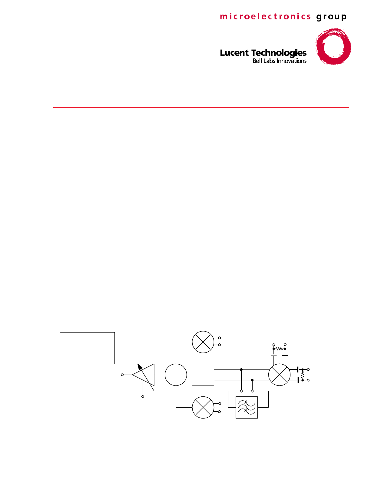
The circuit block diagram is shown in Figure 1. From
two LO signals, LOL and LOH, the offset mixer
produces an internal LO signal, which prevents the
external VCOs from being pulled by the large
transmitted signal. The phase shifter splits the LO
signal into two carriers with 90° phase separation
and equal amplitude.
These signals are fed to the in-phase (I) and
quadrature-phase (Q) double-balanced mixers. The
resulting signals are summed and fed into the output
amplifier. This amplifier can provide 0 dBm linear
output power, minimum, into a 50 Ω load.
The output power can be attenuated up to 50 dB by
applying a control voltage to the APC input.
Nominally, the output power is at maximum
(+3 dBm) with VAPC > 2.2 V, and at minimum
(–50 dBm) with VAPC < 0.8 V.
The W3011 1 GHz Quadrature Modulator is a
monolithic integrated circuit that provides direct
BIAS AND CONTROL
VCC
ENABLE
GROUND
RFOUT
∑
APC
Figure 1. Circuit Block Diagram
A CMOS/TTL-compatible logic input allows the
device to be put into a powerdown mode in which
less than 10 µA of supply current is consumed.
I
–π/4
φ
+π/4
Q
LOH IN
50 Ω
LOL IN
50 Ω
EXTERNAL FILTER
OR
DIRECT LO INPUT
Page 2
W3011 Data Sheet
1 GHz Quadrature Modulator September 1999
Pin Information
1
IP
2
IN
3
QP
QN
4
10
5
6
7
8
9
TOP
VIEW
APC
GND
ENABLE
GND
LC1
LC2
Figure 2. Pin Configuration
Table 1. Pin Descriptions
Pin Name Function
1 IP Differential Baseband Input (in-phase)
2 IN Differential Baseband Input (in-phase)
3 QP Differential Baseband Input (quad-phase)
4 QN Differential Baseband Input (quad-phase)
5 APC Automatic Power Control dc Input
6 GND dc Ground
7 ENABLE Logic Enable
8 GND dc Ground
9 LC1 Differential LO Input/External Filter
10 LC2 Differential LO Input/External Filter
11 LOHN Differential High-frequency Local Oscillator
Input
12 LOHP Differential High-frequency Local Oscillator
Input
13 LOLN Differential Low-frequency Local Oscillator
Input
14 LOLP Differential Low-frequency Local Oscillator
Input
15 GND dc Ground
16 GND dc Ground
17 RFOUT Open-collector RF Output
18 GND dc Ground
19 VCCRF Positive Power Supply for RF Output Stage
20 VCC Positive Power Supply (nonoutput circuits)
20
19
18
17
16
15
14
13
12
11
VCC
VCCRF
GND
RFOUT
GND
GND
LOLP
LOLN
LOHP
LOHN
2 Lucent Technologies Inc.
Page 3
Data Sheet W3011
September 1999 1 GHz Quadrature Modulator
Absolute Maximum Ratings
Stresses in excess of the absolute maximum ratings can cause permanent damage to the device. These are
absolute stress ratings only, as shown in Table 2. Functional operation of the device is not implied at these or
any other conditions in excess of those given in the operations sections of the data sheet. Exposure to absolute
maximum ratings for extended periods can adversely affect device reliability.
Table 2. Absolute Maximum Ratings
Parameter Symbol Min Max Unit
Ambient Operating Temperature TA –35 85 °C
Storage Temperature Tstg –65 150 °C
Lead Temperature (soldering, 10 s) — — 300 °C
Positive Supply Voltage VCC –0.3 4.5 V
Power Dissipation PD — 650 mW
ac p-p Input Voltage Vp-p –0.3 VCC V
Digital Voltages — –0.3 VCC V
Handling Precautions
Although protection circuitry has been designed into this device, proper precautions should be taken to avoid
exposure to electrostatic discharge (ESD) during handling and mounting. Lucent Technologies Microelectronics
Group employs a human-body model (HBM) and a charged-device model (CDM) for ESD-susceptibility testing
and protection design evaluation. ESD voltage thresholds are dependent on the circuit parameters used to define
the model. No industry-wide standard has been adopted for CDM. However, a standard HBM (resistance =
1500 Ω, capacitance = 100 pF) is widely used and, therefore, can be used for comparison purposes. The HBM
ESD threshold presented here was obtained by using these circuit parameters:
ESD Threshold Voltage
Model Rating
HBM 2000
CDM (corner pins)
CDM (noncorner pins)
500
500
Lucent Technologies Inc. 3
Page 4
W3011 Data Sheet
1 GHz Quadrature Modulator September 1999
Operating Ranges
The W3011 operating ranges are shown in Table 3. Performance is not guaranteed over the full range of all
conditions possible within this table. However, the table lists the ranges of external conditions in which the
W3011 provides general functionality, which may be useful in specific applications, without risk of permanent
damage. The conditions for guaranteed performance are described in Tables 4 and 5.
Table 3. Operating Ranges
Parameter Min Max Unit
VCC 2.7 3.6 Vdc
Ambient Operating Temperature –35 85 °C
fLO Direct Mode (pins 9 and 10) 800 1000 MHz
PLO Direct Mode (pins 9 and 10) 110 600 mVp-p
Offset Local Oscillator (LOL) Frequency 50 800 MHz
LOL Input Level –15 –3 dBm
UHF Local Oscillator (LOH) Frequency 100 1300 MHz
LOH Input Level –15 –3 dBm
External dc Bias Voltage for I & Q Inputs with
0.282 Vrms ac Input Level:
Differential ac Input 1.2 VCC – 0.7 Vdc
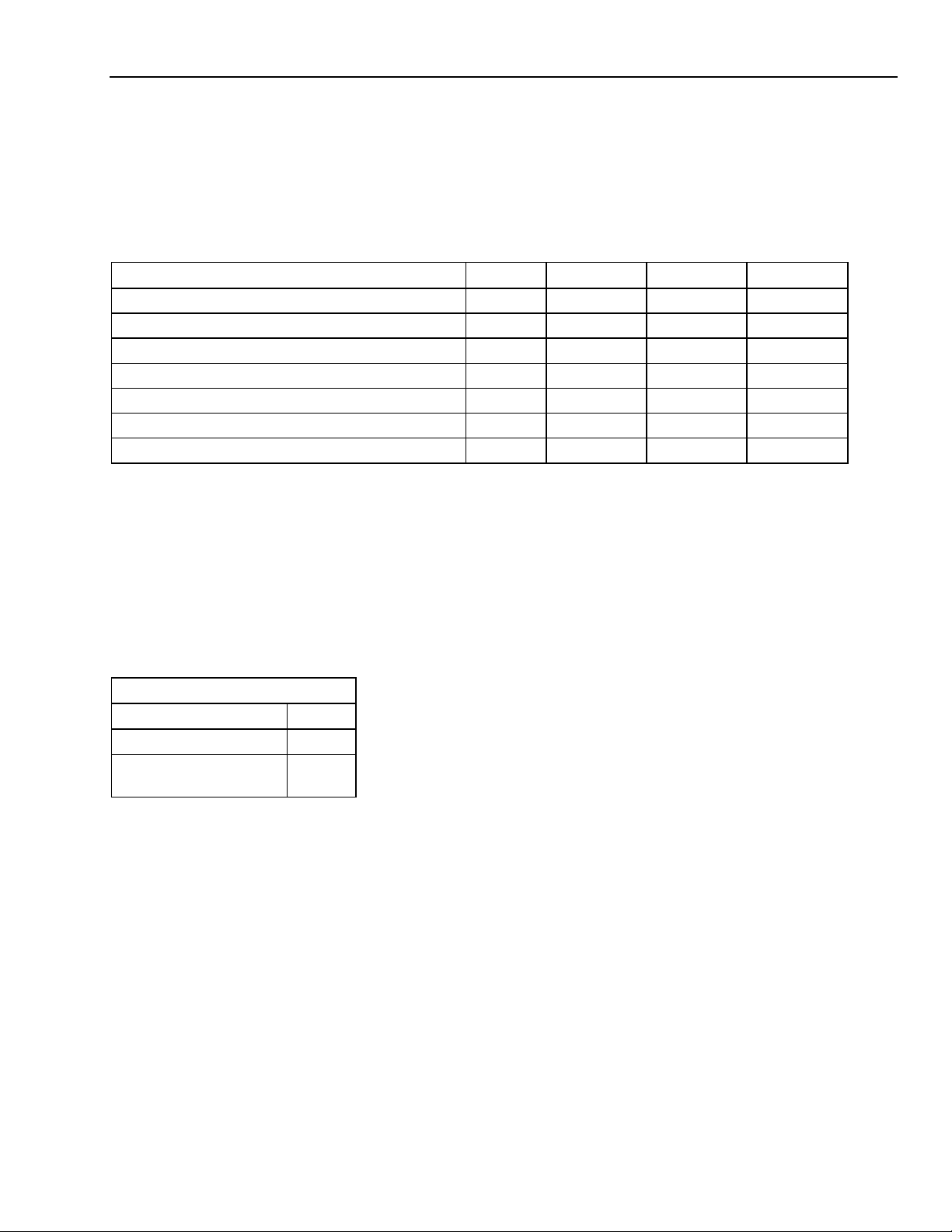
Electrical Characteristics
Table 4. dc and Digital Electrical Specifications
Conditions unless otherwise noted: 2.7 ≤ VCC ≤ 3.3 Vdc; TA = 25 °C ± 3 °C; RL = 50 Ω, VAPC = 2.7 Vdc;
fRF = 900 MHz, fLOL = 130 MHz, fLOH = 1030 MHz, –13 dBm < PLOL, PLOH < –5 dBm;
I – I = 0.4 cos(2πt Ÿ 80 kHz), Q – Q = 0.4 cos(2πt Ÿ 80 kHz – π/2), Vbias of I, I , Q, and Q = 1.22 Vdc.
Parameter Symbol Min Typ Max Unit
Enable Input
Logic High Voltage VIH 0.7 VCC — VCC + 0.4 V
Logic Low Voltage VIL GND – 0.4 — 0.3 VCC V
Logic High Current (VIH = 3.3 V) IIH — — 10 µA
Logic Low Current (VIL = 0.4 V) IIL — — 10 µA
Powerup/down (after ENABLE change) — — — 4 µs
Power Supply Current
Powerdown (ENB = 0) IPDN — 0.3 50 µA
Transmit (ENB = VCC):
(offset mixer on, APC @ max power)
(offset mixer off, APC @ max power)
Transmit (ENB = VCC):
(offset mixer on, APC @ POUT < PMAX – 10
dB)
(offset mixer off, APC @ POUT < PMAX – 10
dB)
ICC(on)
ICC(on)
—
—
—
—
—
—
52
50
46
43
66
64
—
—
mA
mA
mA
mA
4 Lucent Technologies Inc.
Page 5

Data Sheet W3011
September 1999 1 GHz Quadrature Modulator
Electrical Characteristics (continued)
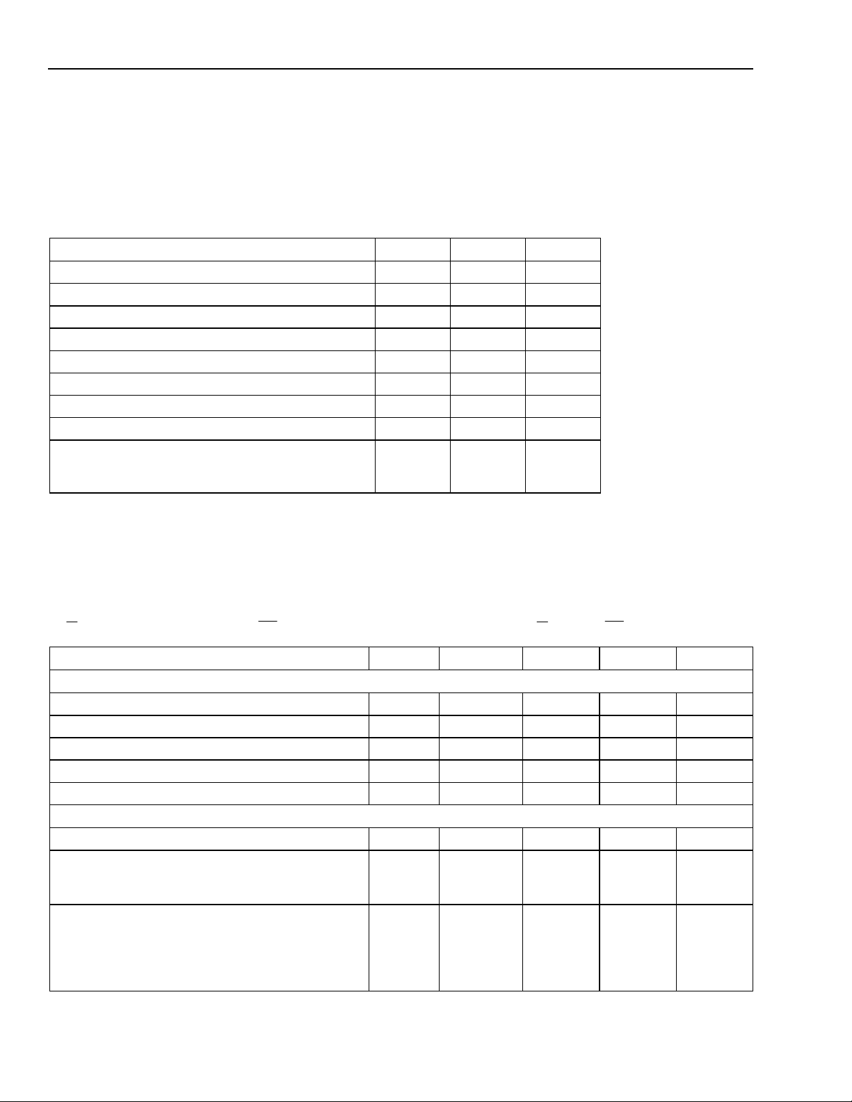
Table 5. ac Specifications
Conditions unless otherwise noted: 2.7 ≤ VCC ≤ 3.3 Vdc; TA = 25 °C ± 3 °C; RL = 50 Ω, VAPC = 2.7 Vdc;
fRF = 900 MHz, fLOL = 130 MHz, fLOH = 1030 MHz, –15 dBm < PLOL, PLOH < –5 dBm;
I – I = 0.4 cos(2πt Ÿ 80 kHz), Q – Q = 0.4 cos(2πt Ÿ 80 kHz – π/2), Vbias of I, I , Q, and Q = 1.22 Vdc.
Parameter Min Typ Max Unit
I & Q
I & Q Signal Path 0.5 dB Bandwidth — 5 — MHz
I & Q Input Resistance — 200 —
I & Q Input Capacitance to Ground — 5 — pF
I & Q Input Differential Signal for Max Output — 0.8 — Vp-p
Offset Mixer
LOL Input Impedance — 50 —
LOH Input Impedance — 50 —
LO Input Impedance (pins LC1, LC2) — 480//1 —
LOL Input IP3 — 10 — dBm
Modulation Accuracy (POUT = –1 dBm)
Carrier Suppression (POUT = –1 dBm) — –35 –28 dBUSB
Carrier Suppression (entire usable APC range) — — –26 dBUSB
Origin Offset (DQPSK inputs, all usable APC levels) — — –23 dBc
Error Vector Magnitude (See Explanation of Error Vector Magnitude
(EVM) Testing section.)
Lower Sideband (LSB) Suppression (See Figure 3.) — –43 –34 dBUSB
RF Output
Output Power (0.8 Vp-p differential or single-ended 80 kHz sine-wave
inputs to I and Q, with 90° between I and Q)
Adjacent Channel Suppression (0.282 Vrms differential I and Q inputs,
π/4 – DQPSK modulation, random data):
Per PDC (RCR STD-27):
±50 kHz, All Usable APC Levels
±100 kHz, All Usable APC Levels
±100 kHz, Max RF Output (APC > 2.2)
Per IS-136/IS-137 800 MHz Digital Mode:
±30 kHz, All Usable APC Levels
±60 kHz, All Usable APC Levels
Noise Floor Suppression, FC ± >100 kHz — –120 –112 dBc/Hz
APC (Automatic Power Control) Function
Range of Usable Output Power Control for Japan PDC (RCR STD-27),
from Max Power at APC = 2.7 V to Minimum APC Voltage Where
Requirements for ACP and Carrier Suppression Are Still Met Using
π/4 – DQPSK/α = 0.5 Modulation at 0.282 Vrms Differential I and Q
Inputs:
Offset Mixer Not Used
Offset Mixer Used
Output Power Variation Due to Temperature, within Usable Control Range — 4 6 dB
RF Power Change Time (after APC change) — — 2 µs
APC Voltage for Max Output Power — 2.2 — Vdc
APC Voltage for Min Output Power — 0.8 — Vdc
— 2.5 5 %
–1 3 — dBm
—
—
—
—
—
29
39
–65
—
–75
–45
–60
40
45
–55
–62
–65
–36
–50
—
—
kΩ
Ω
Ω
Ω//pF
dBc
dBc
dBc
dBc
dBc
dB
dB
Lucent Technologies Inc. 5
Page 6

W3011 Data Sheet
1 GHz Quadrature Modulator September 1999
Explanation of Error Vector Magnitude (EVM) Testing
Error vector magnitude (EVM) is estimated by feeding signals to the W3011 as described above in Table 5.
A typical narrowband, sine-wave modulation output spectrum appears in Figure 3.
0
–10
–20
–30
–40
–50
MAGNITUDE (dBm)
–60
–70
–80
L5
–72 dBm
899.60 899.68 899.76 899.84 899.92 900.08 900.16 900.24 900.32 900.40900
L4
–75 dBm
L3
–48 dBm
L2
–70 dBm
LSB
–38 dBm
Fc
–40 dBm
FREQUENCY (MHz)
Figure 3. W3011 Sine-Wave Modulation Output Spectrum
Data from this spectrum is used to estimate EVM by the formula:
EVM (%) = 100 Ÿ [10
10
P(L5)/20
P(U3)/20
+ 10
+ 10
P(L4)/20
P(U4)/20
+ 10
+ 10
P(L3)/20
P(U5)/20
+ 10
]/10
P(L2)/20
P(USB)/20
USB
0 dBm
+ 10
–50 dBm
P(LSB)/20
U2
+ 10
U3
–72 dBm
P(U2)/20
fl = fQ = 80 kHz
fLOL = 130 MHz
fLOH = 1030 MHz
U5
–62 dBm
U4
–70 dBm
+
The data presented in the spectrum above would yield:
EVM (%) = 100 Ÿ [251e–6 + 178e–6 + 3981e–6 + 316e–6 +
12589e–6 + 3162e–6 + 251e–6 + 316e–6 + 794e–6]/1000e–3
= 2.18%
This approximates worst-case digital modulation results, because the sine-wave modulation estimate assumes all
spurious outputs are in phase and adds their magnitudes as scalars. In addition, this estimate includes fullamplitude measurements of spurious peaks that would appear in adjacent and alternate channels, where a
receiver would otherwise provide attenuation. The L3 third-order intermodulation peak and LSB (lower sideband)
are normally the unwanted output frequencies that dominate the EVM estimate.
6 Lucent Technologies Inc.
Page 7

Data Sheet W3011
September 1999 1 GHz Quadrature Modulator
RFOUT Matching: Basic Open Collector Termination
The W3011 RF output uses an open collector output architecture. To operate properly, this requires that dc bias
current be provided through the output pin (pin 17). Thus, the output matching network must always provide a
shunt dc connection to the positive power supply. Examples of such a connection include a shunt-matching
inductor or a shunt RF choke. Figure 4 illustrates a simple RFOUT matching configuration.
20
19
18
17
VCC
TO TX SAW FILTER
(50 Ω)
Figure 4. W3011 RF Output Diagram
Offset Mixer
W3011 with Offset Mixer Disabled
If the offset mixer in the W3011 is not required for the frequency plan, the offset mixer may be turned off by
connecting the positive supply (VCC) to any or all of pins 11 (LOHN), 12 (LOHP), 13 (LOLN), or 14 (LOLP), as
illustrated in Figure 5 below. Disabling the offset mixer reduces current consumption 2 mA to 3 mA. If pin 11 is
connected to VCC, pins 12, 13, and 14 must be connected to VCC or no-connect (NC). Connect the RF VCO to
either pin 9 or pin 10 through a low-impedance coupling capacitor, and connect the unused pin (10 or 9) through
a similar capacitor to ground.
1
I
20
VCC
Q
APC
ENB
10
OPTIONAL TERMINATION RESISTOR
14
13
12
11
CONNECT VCC TO ANY OF PINS
11—14 TO DISABLE OFFSET
MIXER AND REDUCE POWER
SUPPLY CURRENT
VCC
TO TX SAW FILTER
Figure 5. W3011 Application with Offset Mixer Disabled
Lucent Technologies Inc. 7
Page 8

W3011 Data Sheet
1 GHz Quadrature Modulator September 1999
Offset Mixer (continued)
W3011 Using Offset Mixer
If the W3011 offset mixer is required, two VCOs must be connected (see Figure 6). A low-frequency (VHF)
oscillator may be dc-coupled to either pin 13 (LOLN) or pin 14 (LOLP) if the VCO contains a dc-blocking
capacitor at its output. Otherwise, use a low-impedance series capacitor between the VCO output and the LOL
input. The other LOL pin must be dc-grounded (no external capacitor for the grounded pin). As shown in Figure
1, there is a 50 Ω termination resistor on chip, connected between pins 13 and 14.
In the same way, as shown in Figure 6, one of the pins 11 (LOHN) or 12 (LOHP) must be connected to dc
ground. The other pin is connected to a high-frequency (UHF) VCO, using either dc coupling (if the VCO contains
a dc-blocking capacitor at its output) or a low-impedance series-coupling capacitor. There is also a 50 Ω
termination resistor on chip connected between pins 11 and 12.
When the offset mixer is used, it is necessary to filter the offset mixer output signal with a parallel-tuned LC filter
between pins 9 and 10. The resonant frequency of this filter should be approximately the center of the transmit
RF band (for example, about 920 MHz for PDC 800). The filter should be adjusted for lowest EVM at RFOUT.
VCC
1
I
20
Q
APC
φ
ENB
9
10
14
13
12
11
RFOUT
LOL VCO
LOH (UHF) VCO
Figure 6. W3011 Application Using Offset Mixer
8 Lucent Technologies Inc.
Page 9

Data Sheet W3011
September 1999 1 GHz Quadrature Modulator
Characteristic Curves
Conditions unless otherwise noted: VCC = 2.7; TA = 25 °C ± 3 °C; LOH = 755 MHz @ –12.5 dBm, LOL = 185
MHz @ –12.5 dBm; I/Q= 0.8 Vp-p π/4 – DQPSK; α = 0.5 (random data); I/Q Vcm = 1.22 Vdc; LC filter = 10
nH//2.2 pF; RFOUT = 940 MHz.
V
CC
10
–10
= 2.7
V
CC
= 3.0
V
CC
= 3.3
60
0
55
VCC = 2.7
VCC = 3.0
V
= 3.3
CC
–20
–30
–40
RFOUT (dBm)
–50
–60
–70
0.5 1.0 1.5 2.0 2.5 3.0
APC VOLTAGE (V)
Figure 7. Output Power vs. APC and Supply
Voltage
25 °C
–20 °C
10
0
–10
–20
–30
–40
RFOUT (dBm)
–50
–60
–70
–80
0.5
1.0
1.5 2.0 2.5 3.0
APC VOLTAGE (V)
85 °C
50
45
40
SUPPLY CURRENT (mA)
35
30
–70 –60 –50 –40 –30 –20 –10 0 10
RF OUTPUT (dBm)
Figure 9. Supply Current vs. Output Power
LO = –15 dBm
LO = –10 dBm
50
45
40
35
30
25
20
15
10
5
CARRIER SUPPRESSION (dB)
0
–60 –50 –40 –30 –20 –10
OUTPUT POWER (dBm)
LO = –5 dBm
0
10
Figure 8. Output Power vs. APC Voltage and
Temperature
Figure 10.Carrier Suppression vs. Output
Power and LO Level
Lucent Technologies Inc. 9
Page 10

W3011 Data Sheet
1 GHz Quadrature Modulator September 1999
Characteristic Curves (continued)
5
4.5
4
3.5
3
2.5
2
1.5
1
0.5
ERROR VECTOR MAGNITUDE (%rms)
0
–50 –40 –30 –20
RFOUT (dBm)
Figure 11. EVM vs. Output Power and
Temperature
–10 0
25 °C
–20 °C
85 °C
10
± 50 kHz
10
0
–10
–20
–30
–40
–50
–60
ADJACENT CHANNEL POWER (dB)
–70
–80
–70 –60 –50 –40 –30 –20 –10 0 10
BELOW –30 dBm RF OUTPUT
MEASUREMENT MAY BE LIMITED
BY NOISE FLOOR OF SPECTRUM
ANALYZER.
OUTPUT POWER (dBm)
± 100 kHz
Figure 13. Adjacent Channel Power
Suppression for PDC
1.2 Vdc
1.3 Vdc
10
9
8
7
6
5
4
EVM (%rms)
3
2
1
0
–60 –50 –40 –30 –20 –10 0 10
OUTPUT POWER (dBm)
1.5 Vdc
Figure 12. EVM vs. Output Power and I/Q
Common-Mode Voltage
10 Lucent Technologies Inc.
Page 11

Data Sheet W3011
September 1999 1 GHz Quadrature Modulator
Package Outline
20-Pin TSSOP
Dimensions are in millimeters.
DETAILB
1.00
10 1
11 20
0.65 BSC
6.50 ± 0.10
0.15
MAX
1.00
1.00
6.25/6.5
1.10
MAX
M M
0.254 E
1
0.076 C
SEATING
PLANE
WITH PLATING
BASEMETAL
0.90 ± 0.05
0.19/0.30
0.22
± 0.03
DETAILC
SEEDETAILA
4.3/4.5
-E-
0.090/0.135
0.090/0.20
0.090/0.20
0.25 BSC
SEEDETAILC
8
0.60 ± 0.10
DETAILA
DETAILB
5-5499
Lucent Technologies Inc. 11
Page 12

W3011 Data Sheet
1 GHz Quadrature Modulator September 1999
Manufacturing Information
This device may be assembled in any of the following locations: assembly codes P, M, or T.
Ordering Information
Device Code Description Package Comcode
LUCW3011FCL 1 GHz Quadrature Modulator 20-pin TSSOP 108 131 400
LUCW3011FCL-TR* 1 GHz Quadrature Modulator 20-pin TSSOP, tape and reel 108 131 426
EVB3011 Evaluation Board — 108 131 913
* Contact your Lucent Technologies Microelectronics Group Account Manager for minimum order requirements.
For additional information, contact your Microelectronics Group Account Manager or the following:
INTERNET: http://www.lucent.com/micro
E-MAIL: docmaster@micro.lucent.com
N. AMERICA Microelectronics Group, Lucent Technologies Inc., 555 Union Boulevard, Room 30L-15P-BA, Allentown, PA 18103
ASIA PACIFIC: Microelectronics Group, Lucent Technologies Singapore Pte. Ltd., 77 Science Park Drive, #03-18 Cintech III, Singapore 118256
CHINA: Microelectronics Group, Lucent Technologies (China) Co., Ltd., A-F2, 23/F, Zao Fong Universe Building, 1800 Zhong Shan Xi Road,
JAPAN: Microelectronics Group, Lucent Technologies Japan Ltd., 7-18, Higashi-Gotanda 2-chome, Shinagawa-ku, Tokyo 141, Japan
EUROPE: Data Requests: MICROELECTRONICS GROUP DATALINE: Tel. (44) 7000 582 368, FAX (44) 1189 328 148
ITALY: (39) 02 6608131 (Milan), SPAIN: (34) 1 807 1441 (Madrid)
Lucent Technologies Inc. reserves the right to make changes to the product(s) or information contained herein without notice. No liability is assumed as a result of their use or application. No
rights under any patent accompany the sale of any such product(s) or information.
Copyright © 1999 Lucent Technologies Inc.
All Rights Reserved
Printed in U.S.A.
September 1999
DS99-205WRF (Replaces DS98-016WRF)
1-800-372-2447, FAX 610-712-4106 (In CANADA: 1-800-553-2448, FAX 610-712-4106)
Tel. (65) 778 8833, FAX (65) 777 7495
Shanghai 200233 P.R. China Tel. (86) 21 6440 0468, ext. 316, FAX (86) 21 6440 0652
Tel. (81) 3 5421 1600, FAX (81) 3 5421 1700
Technical Inquiries: GERMANY: (49) 89 95086 0 (Munich), UNITED KINGDOM: (44) 1344 865 900 (Ascot),
FRANCE: (33) 1 40 83 68 00 (Paris), SWEDEN: (46) 8 594 607 00 (Stockholm), FINLAND: (358) 9 4354 2800 (Helsinki),
Printed On
Recycled Paper
 Loading...