

Page 1
Advance Data Sheet
December 1999
W3000 PLL Dual-Band Frequency Synthesizer
Features
+ 2.2 GHz operational
+ Dual-band optimized
+ Low supply current (5.1 mA)
+ Surface-mount 14-pin TSSOP package
+ Scaled PD gain for dual-band operation
+ Programmable phase-detector polarity
+ Synchronous or forced counter update loading
+ Powerdown mode via external pin or serial bus
+ Low-load capacitance on reference input buffer
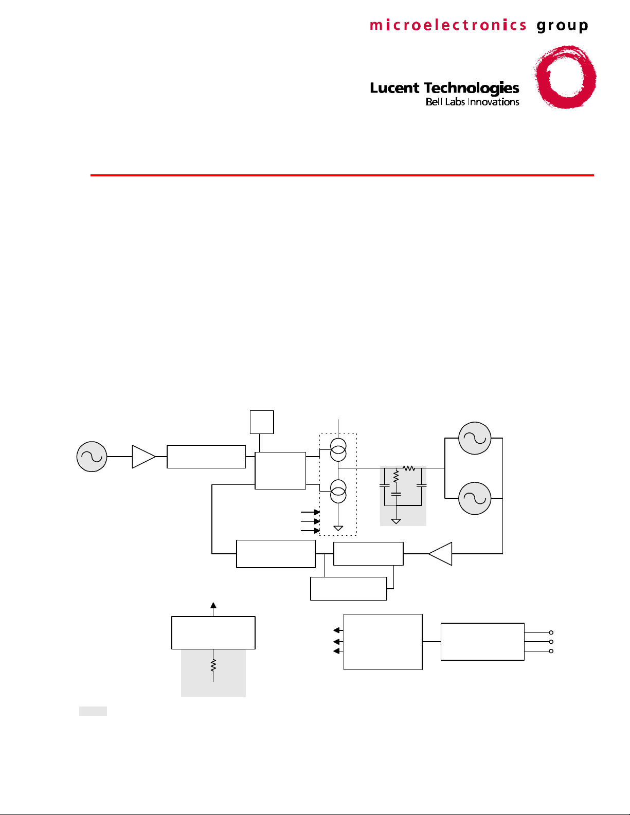
LD
REF_IN
11-BIT COUNTER
TCXO
R
PHASE
DETECTOR
Applications
+ GSM900/1800/1900
+ North American IS-136/137
+ Personal Digital Cellular (Japan RCR-27)
+ Personal Handy Phone (Japan RCR-28)
+ CDMA (IS-95)
VDDC
VCP
VCO BAND A
OFF CHIP
IREF
HIGH-PRECISION
CURRENT
REFERENCE
RREF
VDDC
IPD SETTING
PD POLARITY
11-BIT COUNTER
IREF
M
7-BIT COUNTER
IPD SETTING
PD POLARITY
BAND
PRESCALER
÷
64/65
A
CONTROL
LOGIC
Figure 1. Block Diagram with Pinout
VCO BAND B
MAIN_IN
24-BIT SERIAL
SHIFT REGISTER
LAT
DAT
CLK
Page 2

Advance Data Sheet
W3000 PLL Dual-Band Frequency Synthesizer December 1999
Table of Contents
Features............................................................................................................................................................... 1
Applications .........................................................................................................................................................1
Description...........................................................................................................................................................3
Pin Information.....................................................................................................................................................4
Absolute Maximum Ratings.................................................................................................................................. 5
Electrostatic Discharge Caution............................................................................................................................ 5
Electrical Characteristics...................................................................................................................................... 6
Charge Pump Current..........................................................................................................................................7
PLL Programming Information .............................................................................................................................8
Serial Data Input..................................................................................................................................................9
Serial Bus Timing Information..............................................................................................................................9
Functional Descriptions......................................................................................................................................10
REF Register .....................................................................................................................................................11
MAIN Register....................................................................................................................................................15
PLL Lock-Detect Function..................................................................................................................................17
Typical Performance Characteristics..................................................................................................................17
MAIN_IN Input Parallel Equivalent Circuit.......................................................................................................18
Application Example ..........................................................................................................................................18
Application Information ...................................................................................................................................... 19
Typical Performance Data..................................................................................................................................22
Outline Diagram................................................................................................................................................. 26
14-Pin TSSOP ................................................................................................................................................26
Manufacturing Information ................................................................................................................................. 27
Ordering Information..........................................................................................................................................27
Lucent Technologies Inc.2
Page 3
Advance Data Sheet
December 1999 W3000 PLL Dual-Band Frequency Synthesizer
Description
The W3000 is a high-performance UHF RF PLL synthesizer, designed for use in digital wireless communication
applications. Particular emphasis in the design has been placed on dual-band applications, with near-seamless
switching between operational bands without the need for external loop-filter circuitry other than that required for
single band applications. In combination with a suitable reference crystal, UHF VCO, and associated loop-filter
components, the W3000 offers a very low-noise oscillator solution.
The reference signal is divided by a programmable 11-bit counter to provide a wide range of comparison
frequencies, allowing compliance with the various standards. The reference input is rising-edge triggered, and we
recommend that an inverting buffer be used when the W3000 is interfaced to a commercial TCXO.
The MAIN_IN signal normally associated with the UHF VCO is fed into a dual modulus prescaler (64/65) and is
then divided by the 11-bit main counter to be compared to the output of the reference counter in a digital phase
detector.
The W3000 is implemented with programmable charge-pump currents to allow fast switching between bands for
dual-band applications, without changing the loop filter. The charge pump can be programmed internally, or
externally with a resistor (recommended). Charge pump outputs can be disabled, thereby allowing open-loop
VCO modulation schemes.
With synchronous reloading, the counter reloads a new programmed value when the counter reaches zero. With
forced counter reloading, the reloading occurs when the programmed word is latched in. These techniques can
improve lock time when performing a dual-band hop or in start-up conditions.
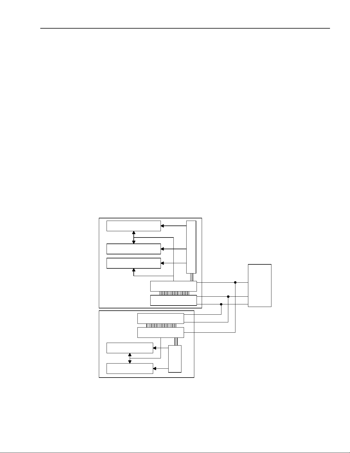
The W3000 uses a standard 3-wire programming bus (data, enable, clock) that operates up to 10 MHz. This
serial interface is via a 24-bit word that incorporates both register addressing and device addressing allowing two
chips to share the bus.
TR REGISTER
CONFIG REGISTER
MAIN REGISTER
W3020
W3000
MAIN REGISTER
A[0:2]
PARALLEL LATCH
SERIAL SHIFT
SERIAL SHIFT
PARALLEL LATCH
ADDRESS DECODER
LAT
CLK
DAT
DAT
CLK
LAT
A[0:2]
SC1
SERLE1
SERCK
SERDA
REF REGISTER
ADDRESS
DECODER
Figure 2. Serial Bus Programming
Lucent Technologies Inc. 3
Page 4
Advance Data Sheet
W3000 PLL Dual-Band Frequency Synthesizer December 1999
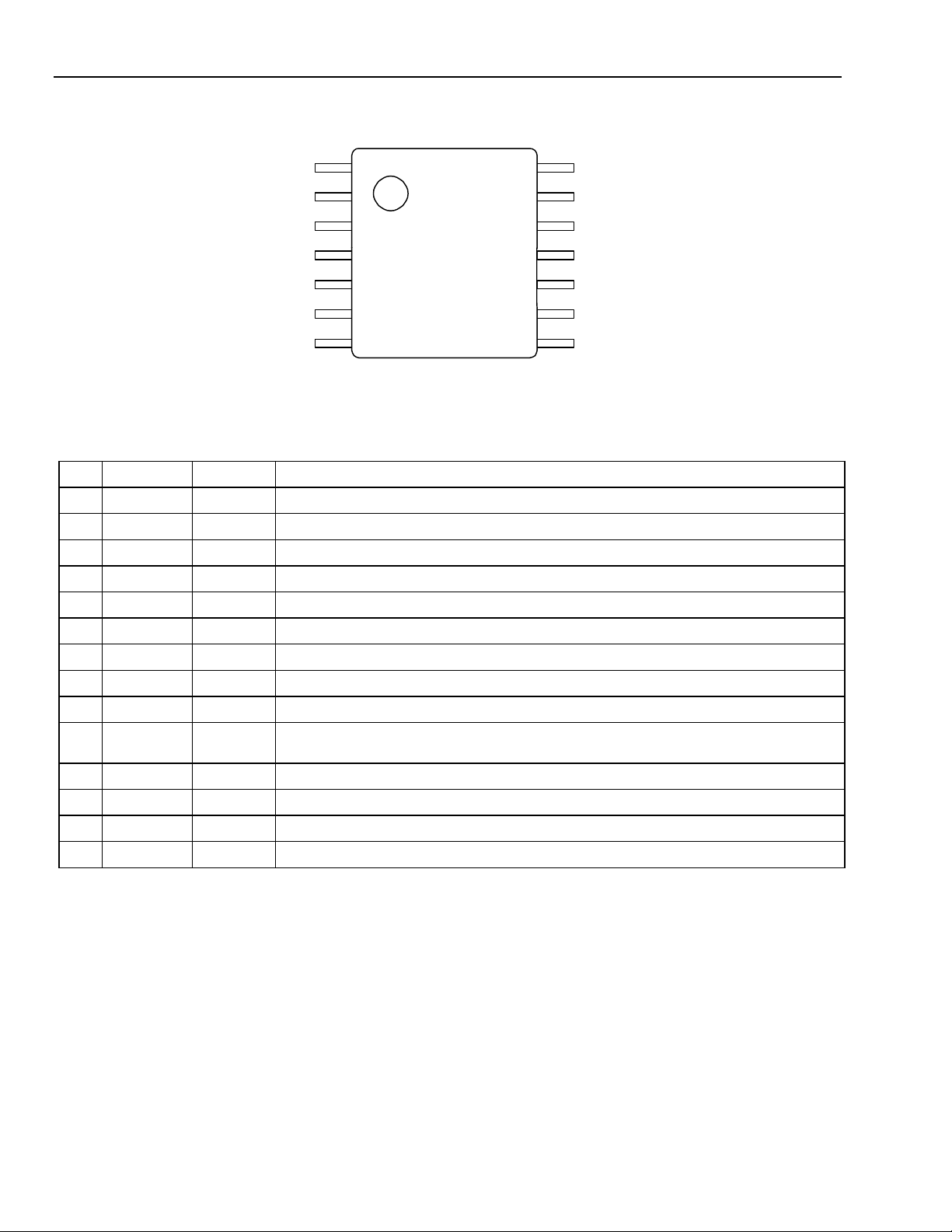
Pin Information
VDDC
CPOUT
VSS1
VSS2
MAIN_IN
VDD1
VDD2
1
2
3
4
5
6
7
14
13
12
11
10
9
8
LAT
DAT
CLK
PWRDN
REF_IN
RES
LOCKDET
Figure 3. Pin Diagram
Table 1. Pin Descriptions
Pin Symbol Function Name/Description
1 VDDC Supply
2 CPOUT Output
3 VSS1 Ground
4 VSS2 Ground
5 MAIN_IN Input
6 VDD1 Supply
7 VDD2 Supply
8 LOCKDET Output
9 RES Input
10 REF_IN Input
Charge Pump Positive Supply Voltage. Must be ≥VDD. (VDD = VDD1 = VDD2).
Charge Pump Output.
Ground 1. Charge pump and logic ground.
Ground 2. Prescaler and reference ground.
VCO Signal Input. Must be ac-coupled.
Voltage Supply 1. Prescaler supply voltage.
Voltage Supply 2. Logic and reference supply (must be equal to VDD1).
Lock Detect Output.
External Resistor Input. Add resistor to VDDC if required (>10 kΩ).
Reference Frequency Input. Connection from reference oscillator. Must be ac-
coupled.
11 PWRDN Input
12 CLK Input
13 DAT Input
14 LAT Input
Powerdown. For low current operation. (Low is powerdown mode.)
Serial Input. Programming clock line.
Serial Input. Programming data line.
Serial Input. Programming latch line.
Lucent Technologies Inc.4
Page 5
Advance Data Sheet
December 1999 W3000 PLL Dual-Band Frequency Synthesizer
Absolute Maximum Ratings
Stresses in excess of the absolute maximum ratings can cause permanent damage to the device. These are
absolute stress ratings only. Functional operation of the device is not implied at these or any other conditions in
excess of those given in the operations sections of the data sheet. Exposure to absolute maximum ratings for
extended periods can adversely affect device reliability.
Parameter Symbol Min Max Unit
Ambient Operating Temperature TA –30 85 °C
Storage Temperature Tstg –65 150 °C
Lead Temperature (soldering, 10 s) TL — 300 °C
Positive Supply Voltage VDD 0 4.5 Vdc
Positive Charge Pump Supply Voltage VDDC 0 4.5 Vdc
Power Dissipation PD — 250 mW
ac Input Voltage — 0 VDD Vp-p
Digital Voltages — Vss – 0.3 VDD + 0.3 Vdc
Electrostatic Discharge Caution
Although protection circuitry has been designed into this device, proper precautions should be taken to avoid
exposure to electrostatic discharge (ESD) during handling and mounting. Lucent Technologies Microelectronics
Group employs a human-body model (HBM) and a charged-device model (CDM) for ESD-susceptibility testing
and protection design evaluation. ESD voltage thresholds are dependent on the circuit parameters used to define
the model. No industry-wide standard has been adopted for CDM. However, a standard HBM (resistance =
1500 Ω, capacitance = 100 pF) is widely used and, therefore, can be used for comparison purposes.
Parameter Model Min Max Unit
ESD Threshold Voltage HBM 1000 — V
ESD Threshold Voltage (corner pins) CDM 1000 — V
ESD Threshold Voltage (noncorner pins) CDM 1500 — V
Lucent Technologies Inc. 5
Page 6
Advance Data Sheet
W3000 PLL Dual-Band Frequency Synthesizer December 1999
Electrical Characteristics
Table 2. General Specifications
Conditions (unless otherwise specified): VDD = 2.7 V; TA = 25 °C ± 3 °C; VREF = 0.25 Vp-p, VDDC = 2.85 V.
Parameters Symbol Min Typ Max Unit
Ambient Operating Temperature TA –30 25 85
Nominal Operating Voltage VDD 2.7 2.85 3.6 V
Nominal Charge Pump Operating Voltage VDDC VDD 2.85 3.6 V
Power Supply Current
Powerdown Current
‡
†
IDD — 5.1 8.0 mA
IDD — 0.1 20
Digital Inputs:
Logic High Voltage VIH 0.7 * VDD VDD VDD + 0.15 V
Logic Low Voltage VIL – 0.3 GND 0.3 * VDD V
Logic High Current (VIH = VDD + 0.15 V) |IIH| — — 10
Logic Low Current (VIL = –0.3 V) |IIL| — — 10
Digital Outputs:
Logic High Voltage (|IOH| = 2 mA) VOH VDD – 0.4 — — V
Logic Low Voltage (|IOL| = 2 mA) VOL — — 0.4 V
† (IDD1 + IDD2 + IDDC) under locked condition, VDDC = 2.85 V; fVCO.= 1200 MHz; fREF = 13 MHz.
‡ (IDD1 + IDD2 + IDDC) VIL = 0 Vdc on all logic input pins.
°C
µA
µA
µA
Table 3. Electrical Specifications
Conditions (unless otherwise specified): VDD = 2.7 V; TA = 25 °C ± 3 °C; VREF = 0.25 Vp-p, VDDC = 2.85 V.
Parameter Symbol Min Typ Max Unit
Main Input Frequency Range fVCO 0.5 — 2.2 GHz
Main Input Level (1100 MHz—1750 MHz) VMAIN –20 — 6
Main Input Level
†
VMAIN –10 — 6
dBm/50 Ω*
dBm/50 Ω*
Reference Input Frequency Range fREF 8 — 30 MHz
Reference Input Shunt Resistance — 20 30 —
kΩ
Reference Input Shunt Capacitance — — 1.2 3 pF
Reference Input Slew Rate — 41 60 — mV/ns
Reference Input Level VREF 0.25 — 2.00 Vp-p
Phase Detector Comparison Frequency fCOMP 0.025 — 2 MHz
External Resistor Value (pin 9 to VDDC) — 10 18 —
Phase Detector Range —
Phase Detector Noise Floor, ±150 Hz
offset (25 kHz comparison frequency)
*Equivalent voltage of a 50 Ω terminated source.
† Frequencies outside the 1100 MHz—1750 MHz range and up to and including 2200 MHz.
‡ fVCO = 1190 MHz; VREF = 1.4 Vp-p.
‡
— — –167 — dBc/Hz
–2 π
—
2 π
kΩ
rad.
Lucent Technologies Inc.6
Page 7
Advance Data Sheet
December 1999 W3000 PLL Dual-Band Frequency Synthesizer
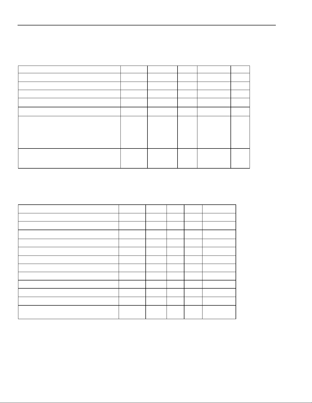
Charge Pump Current
ICP-DN (T = 25 °C )
A
B
C
D
E
F
ICP/mA
COMPLIANCE
RANGE
0.4 V
ICP-UP (T = 25 °C )
COMPLIANCE
RANGE
VDDC – 0.4 V
0.4 2.45
A: CP UP CURRENT AT VCP = VDDC – 0.4.
B: CP UP CURRENT AT VCP = VDDC/2.
C: CP UP CURRENT AT VCP = 0.4.
VDDC/2
VCP
D: CP DOWN CURRENT AT VCP = 0.4 V.
E: CP DOWN CURRENT AT VCP = VDDC/2.
F: CP DOWN CURRENT AT VCP = VDDC – 0.4.
Figure 4. Charge Pump Current vs. Voltage
Table 4. Charge Pump Specifications
Conditions (unless otherwise specified): VDD = 2.7 V; TA = 25 °C ± 3 °C; VDDC = 2.85 V; VCP = VDDC/2;
RREF = 18 kΩ.
Parameter
Charge Pump Output Current
Conditions Symbol Min Typ Max Unit
ICP = 0.7 mA IUP 0.6 0.7 0.8 mA
ICP= 0.7 mA IDN –0.8 –0.7 –0.6 mA
ICP = 0.9 mA IUP 0.8 0.9 1.0 mA
ICP = 0.9 mA IDN –1.0 –0.9 –0.8 mA
ICP = 1.9 mA IUP 1.6 1.9 2.2 mA
ICP = 1.9 mA IDN –2.2 –1.9 –1.6 mA
ICP = 2.5 mA IUP 2.1 2.5 2.9 mA
ICP = 2.5 mA IDN –2.9 –2.5 –2.1 mA
CP High-Impedance State
Current
CP Sink vs. Source Mismatch
CP Current vs. Voltage
2
0.4 < VCP < VDDC – 0.4 V,
–30 °C < TA < +85 °C
1
TA = 25 °C — — 3 15 %
0.4 < VCP < VDDC – 0.4 V,
ITRI — 0.1 20 nA
— — 2 8.5 %
TA = 25 °C
CP Current vs Temperature
Notes (refer to Figure 4 for definitions):
1. ICP-DN vs ICP-UP = charge pump output current up vs down mismatch = [|E| – |B|]/[ 1/2 * {|E| + |B|}] * 100%.
2. ICP vs VCP = charge pump output current magnitude variation vs voltage = [ 1/2 * {|F| – |D|}]/[1/2 * {|F| +|D|}] * 100% and
[1/2 * {|A| - |C|}]/[1/2 *{|A| + |C|}] * 100%.
3. ICP vs TA = charge pump output current magnitude variation vs. temperature = [|E @ temp| – |E @ 25 °C|]/|E @ 25 °C| * 100% and [|B @
temp| – |B @ 25 °C|]/|B @ 25°C| * 100%.
3
–30 °C < TA < +85 °C — — 8 10 %
Lucent Technologies Inc. 7
Page 8

Advance Data Sheet
[
]
f
M
A
f
R
[
]
[
]
W3000 PLL Dual-Band Frequency Synthesizer December 1999
PLL Programming Information
The oscillator frequency is selected according to the following expression:
f*A)M* P(
REF
f
VCO
=
where:
VCO = VCO frequency
P/(P + 1) = Dual modulus prescaler
= Programmable counter ratio (2 to 2047), M > A
= Swallow counter ratio (0 to M – 1 or 127)
REF = External reference oscillator frequency
= Reference counter ratio (2 to 2047)
Example
You wish to have a VCO operating at 1172 MHz, ability to step the frequency in 200 kHz steps, and a reference
clock at 13 MHz.
+
R
Step 1:
Calculate the reference counter ratio R
64
MHz 13
=
91
=
R ==
Step 2: Calculate M & A
f
VCO
1172+=
5860
M is an integer, and so is A; therefore, M = 91, and A = 36.
65
kHz 200
f* A)M* P(
REF
+
R
13* A)M* 64(
65
65*1172
)AM*64( ==+
36
64
13
5860
Lucent Technologies Inc.8
Page 9
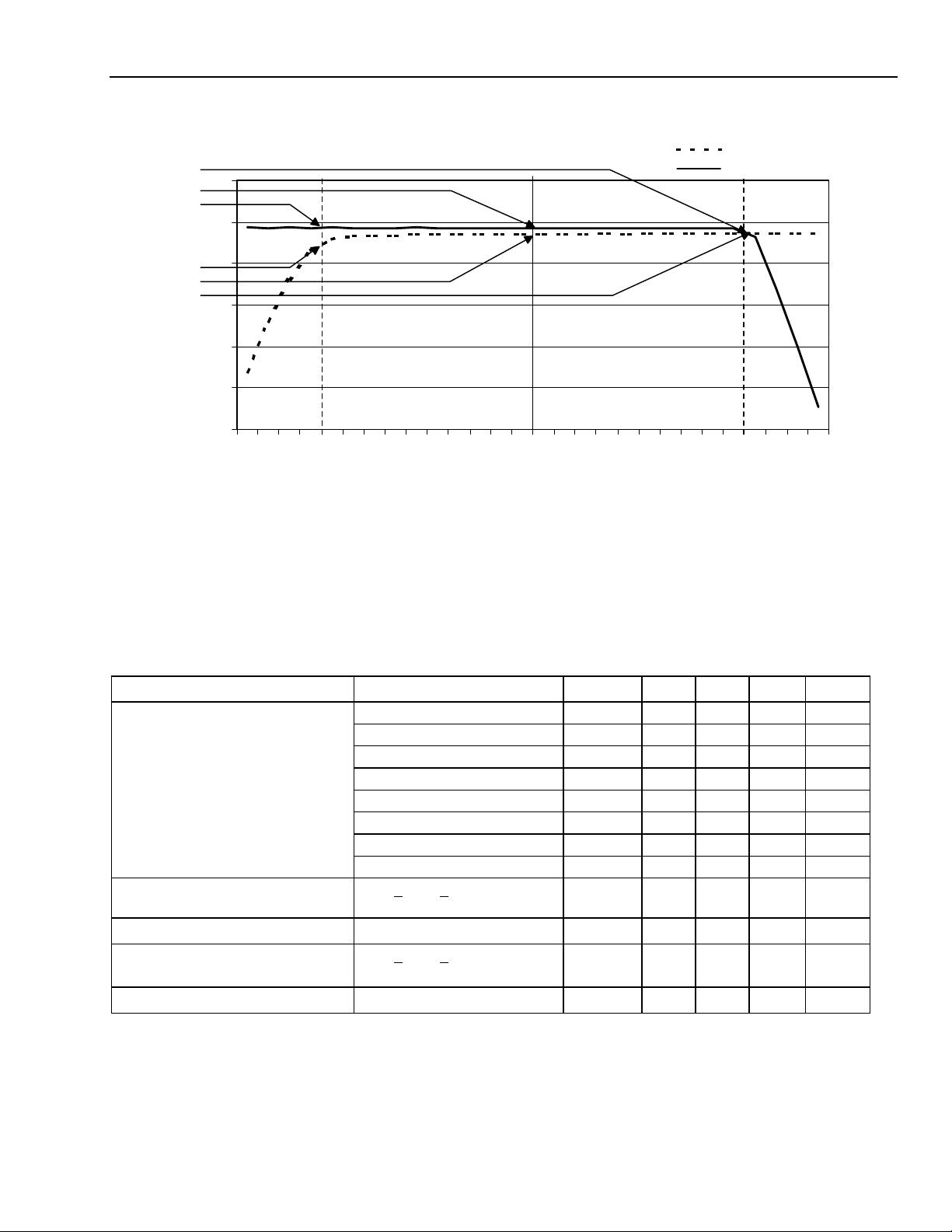
Advance Data Sheet
LSB
tLLt
CWHtCWL
December 1999 W3000 PLL Dual-Band Frequency Synthesizer
Serial Data Input
The PLL is programmed via a 3-wire serial bus, utilizing a data pin (DAT), a clock pin (CLK), and a latch pin
(LAT).
Serial Bus Timing Information
DAT
MSB
CLK
LAT
CS
t
MSB – 1
CH
t
LS
t
OR
LAT
V
LWH
t
Figure 5. Serial Bus Timing Diagram
Table 5. Serial Bus Timing Information
Symbol Parameter Min Typ Max Unit
tCS Data to Clock Setup Time 33 — — ns
tCH Data to Clock Hold Time 10 — — ns
tCWH Clock Pulse Width High 33 — — ns
tCWL Clock Pulse Width Low 33 — — ns
tLS Clock Falling Edge to Latch High Setup Time 0 — — ns
tLWH Latch Pulse Width 50 — — ns
tLL Latch to Clock Setup Time 33 — — ns
fCLK Clock Input Frequency — — 10 MHz
Lucent Technologies Inc. 9
Page 10

Advance Data Sheet
W3000 PLL Dual-Band Frequency Synthesizer December 1999
Functional Descriptions
The W3000 contains a reference register (REF) and a
main register (MAIN). The REF register is used for
programming the division ratio of the reference clock
and for initial setup of the operation modes. The MAIN
register is intended for programming that can occur
frequently, e.g., dynamic channel switching and
putting the W3000 into power-saving mode.
LAT
DAT
CLK
SHIFT REGISTER
Figure 6. Register Programming Diagram
ADDRESS
DECODER
MAIN
REF
Both REF and MAIN registers are programmed
separately, each with a 24-bit data sequence. The last
bit is that which immediately precedes a low-to-high
latch input transition occurring while the CLOCK input
is low. Bit 24 is loaded first, and bit 1 is loaded last.
The last bit in the serial sequence is C0. This bit is
used to direct the 24-bit sequence to the MAIN or REF
registers.
Table 6. C0:C1: MAIN and REF Register
Addressing (Destination of Serial Data)
(Bits 1 and 24)
C1 C0 Addressed Register
0 0 MAIN
0 1 REF
1 0 Secondary Address
1 1 Secondary Address
The first bit, C1, allows the W3000 to share the serial
bus. When C1 is a logic high, the W3000 ignores the
data sent on the serial bus.
Lucent Technologies Inc.10
Page 11

Advance Data Sheet
December 1999 W3000 PLL Dual-Band Frequency Synthesizer
REF Register
This section describes each bit of the reference register. The REF register is used for programming the division
ratio of the reference clock and for initial setup of the operation modes.
Table 7. REF Register Bit Description (C0 = 1, C1 = 0)
Bit Name Description
1 C0 = 1 Register address bit. C0 = 1 for REF (last bit in serial sequence).
2:12 R[1:11] Reference frequency divide ratio.
13 D1 Forced counter reload programming (synchronous/asynchronous).
14 D2 Charge pump disable function.
15:16 D3, D4 Programable charge pump current for frequency band 2.
17 D5 Phase detector polarity.
18:19 D6, D7 Programable charge pump current for frequency band 1.
20 RE Reset for first programming after powerup (1 = reset).
21 ERES Enables external resistor (on RES pin) to set charge pump current.
22 EN1 Enable W3000. (0 is powerdown.)
23 LD Lock detect output enable.
24 C1 = 0 Secondary address bit (first bit in serial sequence).
Table 8. REF Register
Last bit in serial sequence
1 2 3 4 5 6 7 8 9 10 11 12 13 14 15 16 17 18 19 20 21 22 23 24
C0
= 1R1R2R3R4R5R6R7R8R9R10R11D1D2D3D4D5D6D7
First bit in serial sequence
RE ERES EN LD C1
Table 9. R1:R11: Reference Divider Ratio (Bits 2 to 12)
R11 R10 R9 R8 R7 R6 R5 R4 R3 R2 R1 Divide Ratio R
— — — — — — — — — — — —*
0 0 0 0 0 0 0 0 0 1 0 2
0 0 0 0 0 0 0 0 0 1 1 3
.
.
.
.
.
.
.
.
.
.
.
.
.
.
.
.
.
.
.
.
.
.
.
.
.
.
.
.
.
.
.
.
.
.
.
.
1 1 1 1 1 1 1 1 1 1 1 2047
*The reference counter cannot operate with division numbers less than 2.
= 0
Lucent Technologies Inc. 11
Page 12

Advance Data Sheet
W3000 PLL Dual-Band Frequency Synthesizer December 1999
REF Register (continued)
Table 10. D1: Forced Counter Reload (Bit 13)
D1 Response
0 Synchronous counter reloading update
1 Forced counter reload (M, R, A)
With synchronous reloading, the counter reloads a new programmed value when the counter reaches zero. With
forced counter reloading, the reloading occurs when the programmed word is latched in. This can improve lock
time when performing a dual-band hop.
Table 11. D2: Charge Pump Off Mode (Bit 14)
D2 Response
0 Charge pump enabled
1 Charge pump off (high impedance)
This allows the disabling of the charge pump for systems that directly modulate an open-loop VCO.
Table 12. Band and Charge Pump Current (Band 1, Bits 18 and 19; Band 2, Bits 15 and 16)
Band D3
Bit 15D4Bit 16D6Bit 18D7Bit 19
1 x x 0 0 0.7 mA
1 x x 1 0 0.9 mA
1 x x 0 1 1.9 mA
1 x x 1 1 2.5 mA
2 0 0 x x 0.7 mA
2 1 0 x x 0.9 mA
2 0 1 x x 1.9 mA
2 1 1 x x 2.5 mA
The charge pump current is selected by bit 23 of the MAIN register. Setting bit 23 to a 0 will select band 1, which
is established with bits 18 and 19 of the REF register. Likewise, setting bit 23 to a 1 will select band 2, which is
established with bits 15 and 16 of the REF register. This allows the charge pump current to be dynamically
changed along with the VCO frequency.
The PLL loop natural frequency is proportional to charge pump current and inversely proportional to the N count.
Therefore, when the ratio of charge pump current and VCO frequency is the same, the loop natural frequency
does not change. This allows the same loop filter to be used for two different VCO frequencies. For example, in a
GSM900/1800 system with VCOs running at 1190 MHz/1570 MHz, the current could be set to 1.9 mA for
GSM900 and 2.5 mA for GSM 1800 to compensate for the change in division ratios. The current setting may also
be determined by an external resistor. (See Table 15.) In that case, the ratio between the currents programmed
will stay the same, but the absolute level will be resistor-dependent.
Charge Pump Current
ISET
Lucent Technologies Inc.12
Page 13

Advance Data Sheet
December 1999 W3000 PLL Dual-Band Frequency Synthesizer
REF Register (continued)
Table 13. D5: Phase Detector Polarity (Bit 17)
D5 Phase Detector Polarity
0 Negative slope
1 Positive slope
The phase detector can be programmed for either a negative or positive slope to accommodate the VCO and
low-pass filter characteristics. (See Figure 7.)
1
0
REFERENCE
W3000
LOOP
FILTER
VCO
FREQUENCY
VCO OUTPUT
VCO INPUT CONTROL
VOLTAGE
Figure 7. Programming the Phase Detector Slope
Table 14. RE: Reset (Bit 20)
RE Response
0 Operation mode
1 Reset MAIN and secondary registers
After the power supply is turned on, the REF register must be programmed with a reset. This must be followed by
a programming of the MAIN register before or at the enabling of the PLL circuit.
The RE bit will clear itself, and is required to ensure correct initialization of the IC. This results in the following
conditions:
+ The RE bit is cleared back to 0.
+ The device is in powerdown mode, since the EN[1:2] bits are also cleared.
+ Previous reference and main counter values are maintained.
Lucent Technologies Inc. 13
Page 14

Advance Data Sheet
W3000 PLL Dual-Band Frequency Synthesizer December 1999
REF Register (continued)
Table 15. ERES: External Resistor Setting for Charge Pump Current (Bit 21)
ERES External Resistor Status
0
1
If bit 21 is set to 0, the W3000 uses its internal current source to set the charge pump currents, with the values
shown in Table 12. If bit 21 is set to 1, the charge pump current is set by an external resistor between pin 9
(RES) and VDDC. In this case, the charge pump current is given by the following formula:
Use internal charge pump current setting (not tested in production)
Use external resistor to set charge pump current (recommended)
=
where
ICP = Nominal charge pump current.
ISET = Current setting as in Table 12.
RREF = Value of external current reference resistor. See Table 3 for appropriate value.
A tight-tolerance RREF resistor is recommended.
Table 16. EN1: Synthesizer Enable (Bit 22)
PWRDN
(Input Pin 11)
High 0 Powerdown
High 1 Enable
Low 0 Powerdown
Low 1 Powerdown
The MAIN register also contains an enable bit, EN2. The W3000 is enabled and powered down with either the
REF or the MAIN register, whichever was programmed more recently. The contents of the MAIN and REF
registers are maintained in powerdown mode, providing supply voltages are maintained.
µ
DDC
SETCP
*II
05.1V
−
REF
R *A 100
EN1 Mode
Table 17. LD: Lock Detect Enable (Bit 23)
LD (Bit 23) Mode PLL Condition Output Level on Pin 8 LockDet
0 Disabled Locked High
0 Disabled Unlocked High
1 Enabled Locked High
1 Enabled Unlocked Low
Lucent Technologies Inc.14
Page 15

Advance Data Sheet
December 1999 W3000 PLL Dual-Band Frequency Synthesizer
MAIN Register
The MAIN register is intended for programming that can occur frequently for dynamic channel switching and
putting the W3000 into power-saving mode.
Table 18. MAIN Register Bit Description (C0 = 0, C1 = 0)
Bit Name Description
1 C0 = 0 Register address bit. C0 = 0 for MAIN (last bit in serial sequence).
2:8 A[1:7] Swallow counter for prescaler modulus control.
9:19 M[1:11] Main counter.
20 Reserved —
21 Reserved —
22 EN2 Enable all PLL circuits (0 = powerdown mode).
23 B Band select for charge pump current control (band 1 = 0, band 2 = 1).
24 C1 = 0 Secondary address bit.
Table 19. MAIN Register
Last bit in serial sequence
First bit in serial sequence
1 2 3 4 5 6 7 8 9 10 11 12 13 14 15 16 17 18 19 20 21 22 23 24
C0
= 0A1A2A3A4A5A6A7M1M2M3M4M5M6M7M8M9M10M11
Note: X bits are don’t care bits.
X X EN B C1
Table 20. A1:A7: Swallow Counter Count (Bits 2 to 8)
A7
Bit 8
A6
Bit 7
A5
Bit 6
A4
Bit 5
A3
Bit 4
A2
Bit 3
A1
Bit 2
Counter Ratio
0 0 0 0 0 0 0 0
0 0 0 0 0 0 1 1
0 0 0 0 0 1 0 2
.
.
.
.
.
.
.
.
.
.
.
.
.
.
.
.
.
.
.
.
.
.
.
.
0 1 1 1 1 1 1 63
.
.
.
.
.
.
.
.
.
.
.
.
.
.
.
.
.
.
.
.
.
.
.
.
1 1 1 1 1 1 1 127
= 0
Lucent Technologies Inc. 15
Page 16

Advance Data Sheet
W3000 PLL Dual-Band Frequency Synthesizer December 1999
MAIN Register (continued)
Table 21. M1:M11: Programmable Main Counter Divide Ratio (Bits 9 to 19)
M11
Bit 19
0 0 0 0 0 0 0 0 0 1 0 2
0 0 0 0 0 0 0 0 0 1 1 3
.
.
.
0 0 0 1 1 1 1 1 1 1 1 255
.
.
.
1 1 1 1 1 1 1 1 1 1 1 2047
The main counter divides the frequency of the prescaler output signal and sources the divided signal to the
phase comparator.
Table 22. EN2: Synthesizer Enable (Bit 22)
PWRDN EN2 Mode
M10
Bit 18M9Bit 17M8Bit 16M7Bit 15M6Bit 14M5Bit 13M4Bit 12M3Bit 11M2Bit 10M1Bit 9
.
.
.
.
.
.
H 0 Powerdown
H 1 Enable
L 0 Powerdown
L 1 Powerdown
.
.
.
.
.
.
.
.
.
.
.
.
.
.
.
.
.
.
.
.
.
.
.
.
.
.
.
.
.
.
.
.
.
.
.
.
.
.
.
.
.
.
Divide
Ratio
M
.
.
.
.
.
.
.
.
.
.
.
.
.
.
.
.
.
.
The REF register also contains an enable bit, EN1 (see Table 16). The W3000 is enabled or powered down with
either the REF or MAIN register, whichever was programmed more recently. The contents of the MAIN and REF
registers are maintained in powerdown mode, providing supply voltages are maintained.
Table 23. B: Band Select (Bit 23)
B Band
0 Band 1
1 Band 2
In dual-band operation, this bit allows the use of one loop filter by setting the charge pump current to correspond
to the frequency of the band selected. See Table 12 for the available charge pump current settings.
Lucent Technologies Inc.16
Page 17

Advance Data Sheet
December 1999 W3000 PLL Dual-Band Frequency Synthesizer
PLL Lock-Detect Function
The W3000 provides a basic lock-detect function for fault finding or for system specification requirements.
Inside the W3000, the length of the up or down pulses applied to the loop filter is compared with a reference
clock period. If the current pulses are shorter than a reference clock period for 15 consecutive comparison
periods, the LD line is asserted. If a current pulse is detected that is longer than a reference clock period, the LD
line is unset.
The LD line gives a signal to indicate a PLL fault condition. It does not provide a true loop-locked output. For
example, in a GSM system with a reference clock of 13 MHz and a comparison frequency of 200 kHz, the
current pulses only have to be less than 1/65 of a cycle for 15 consecutive times for the LD line to be asserted.
This equates to ~0.4º of phase. In the worst case, if the phase stays inside this limit, moving from one extreme to
the other, the frequency will only be within 0.2%, i.e., 4 MHz on a 2 GHz VCO.
The LD output from the W3000 is a standard logic signal and requires no external comparison or R-C filters.
Typical Performance Characteristics
CURRENT
METER
VDDC/2
+VDDC
100 pF
LAT
DAT
CLK
PWRDN
REF_IN
RES
LOCK DET
0.01 µF
RREF = 18 k
REFERENCE
SOURCE
50
µC
VDDC
Ω
Ω
UHF
SOURCE
50
VDDC
CPOUT
442
Ω
0.047 µF
6.8 pF
+VDD
Ω
100 pF
VSS1
VSS2
MAIN_IN
VDD1
VDD2
10 MHz REF
Figure 8. MAIN_IN and REF_IN Sensitivity Test Circuit Diagram
MAIN_IN and REF_IN are set to cause a small beat frequency at the phase detector input. This generates a
sawtooth signal at the charge pump output of known slope. The amplitude of the UHF source is decreased. The
sensitivity limit is reached when the slope of this waveform deviates from the calculated value. This is then
repeated for the reference source.
Lucent Technologies Inc. 17
Page 18

Advance Data Sheet
W3000 PLL Dual-Band Frequency Synthesizer December 1999
MAIN_IN Input Parallel Equivalent Circuit
The input impedance is high, and can best be
represented by the model shown in Figure 9.
MAIN_IN
RC
Figure 9. MAIN_IN Parallel Equivalent Circuit
Application Example
2.85 V
15 k
Ω
3 k
150 pF
VCO
Ω
10 nF
33 pF33 pF
1 nF
2.85 V
VDDC
Table 24. MAIN_IN Input Parallel Equivalent
Circuit Values
Frequency (MHz) C (pF)
R (ΩΩ)
600 0.88 3680
800 0.87 2650
1000 0.85 2370
1200 0.85 1970
1400 0.86 1580
1600 0.92 1230
1800 1.00 740
2000 1.10 590
2200 1.20 480
1
VDDC
2
CPOUT
3
VSS1
4
VSS2
5
MAIN_IN
6
VDD1
7
VDD2
PWRDN
REF_IN
LOCKDET
LAT
DAT
CLK
RES
14
13
12
11
10
µ
C
1 nF
9
8
RREF
18 k
Ω
VDDC
50
100 pF
50
Ω
Ω
REF.
OSCILLATOR
Figure 10. Application Circuit Diagram
Lucent Technologies Inc.18
Page 19

Advance Data Sheet
December 1999 W3000 PLL Dual-Band Frequency Synthesizer
Application Information
A typical PLL system can be modeled as follows:
fREF 1/R
KPD = Phase detector in mA/2π rad
Z(s) = Loop filter
KVCO = VCO gain in MHz/V
N = Total divide ratio
R = Reference divide ratio
Where the open loop gain is:
G(s)
OPEN
=
Kvco*)s(Z*KPD
Ns
Where
s = jω
+ KPD Z(s)
1/N
Figure 11. Typical PLL Model
KVCO
s
fVCO
The circuit shown in Figure 12 uses a passive third-order loop filter for the element Z(s), defined by the network:
CHARGE PUMP
OUTPUT
C1
R2
VCO
R1 C3
C2
Figure 12. Third-Order Loop Filter
The purpose of the loop filter is to provide response with bandwidth sufficient not only to allow a quick lock time
but also to meet phase-noise and reference sideband requirements. Addition of a third pole formed by R2 and C3
will improve reference sideband performance with little overall impact on the loop performance. A reasonable
practical limit is that the f comparison is greater than 5 times loop bandwidth.
Lucent Technologies Inc. 19
Page 20

Advance Data Sheet
φ
ω
ω
1R * 22R≥
W3000 PLL Dual-Band Frequency Synthesizer December 1999
Application Information (continued)
General rules for the values of these components have been derived many times
for reference. If:
tansec
1T
=
2T
=
2
c
3T
=
π
φ−φ
ω
p
1
)3T1T(*
+ω
20/attn
110
−
2
REF
)F*2(
where
= Phase margin required, normally 45° for a critically damped response.
= Loop bandwidth.
p
= Loop bandwidth modified for extra pole of R3 and C3, as described by:
c
+φ
=ω 1
c
2
++
T3) (T1 * tan
( )
+
1*
T3*T1 T3) (T1
[ ]
2
++
+φ
( )
)3T1T(*tan
3T*1T)3T1T(
−
2
fREF = Reference frequency.
1
, and are quoted here merely
atten = Attenuation provided by the third pole at the reference frequency.
The loop filter values can then be derived as:
2/1
2
)3T*1)(1T*1(
1C
1R =
PD
1T
*
=
2T
* 1C2C
Kvco*K
2
ω
c
2T
−= 1
1T
*
N*
ω+
2
c
2
22
c
)2T*1(
2
ω+ω+
c
2T
2C
The final pole, consisting of R2 and C3, should be chosen such that the following guidelines are followed:
1C
3C ≤ and
10
1. Rohde, Ulrich L., Digital PLL Frequency Synthesizers Theory and Design, Prentice-Hall, 1983.
Lucent Technologies Inc.20
Page 21

Advance Data Sheet
December 1999 W3000 PLL Dual-Band Frequency Synthesizer
Application Information (continued)
For example, take a GSM application where a loop bandwidth of 22 kHz is required.
Other parameters specified by the system are listed below:
Parameter Value
VCO Gain (KVCO) 88 MHz/V
Charge Pump Current (ICP) 2.5 mA
Divider Ratio (value of midband frequency used) (N) 7850
Required Phase Margin 45°
Reference Frequency Attenuation from Additional Pole 20 dB
Using the formulas above, the three time constants can be calculated as follows:
T1 = 2.63697E – 10–6 s
T2 = 3.14484E – 10–5 s
T3 = 2.38732E – 10–6 s
From these values, we can derive the initial component values as follows:
R1 = 2992 Ω
C1 = 0.96 nF
C2 = 10.5 nF
If we choose R2 = 15 kΩ, then
C3 = 159 pF
From these initial values, the loop filter components used in the application circuit can be derived through
practical optimization.
Lucent Technologies Inc. 21
Page 22

Advance Data Sheet
W3000 PLL Dual-Band Frequency Synthesizer December 1999
Typical Performance Data
DN (–30 °C)
UP (–30 °C)
3000
2500
2000
1500
1000
CP CURRENT (µA)
500
0
0 0.5 1 1.5 2 2.5 3
APPLIED CP VOLTAGE (V)
DN (25 °C)
UP (25 °C)
DN (85 °C)
UP (85 °C)
Figure 13. Charge Pump Current vs. Voltage and
Temperature (2.5 mA)
800
700
DN (–30 °C)
UP (–30 °C)
DN (25 °C)
UP (25 °C)
DN (85 °C)
UP (85 °C)
DN (–30 °C)
UP (–30 °C)
1200
1000
800
600
400
CP CURRENT (µA)
200
0
0 0.5 1 1.5 2 2.5 3
APPLIED CP VOLTAGE (V)
DN (25 °C)
UP (25 °C)
DN (85 °C)
UP (85 °C)
Figure 15. Charge Pump Current vs. Voltage and
Temperature (0.9 mA)
2500
DN (–30 °C)
UP (–30 °C)
DN (25 °C)
UP (25 °C)
DN (85 °C)
UP (85 °C)
600
500
400
300
CP CURRENT (µA)
200
100
0
0 0.5 1 1.5 2 2.5 3
APPLIED CP VOLTAGE (V)
Figure 14. Charge Pump Current vs. Voltage and
Temperature (0.7 mA)
2000
1500
1000
CP CURRENT (µA)
500
0
0 0.5 1 1.5 2 2.5 3
APPLIED CP VOLTAGE (V)
Figure 16. Charge Pump Current vs. Voltage and
Temperature (1.9 mA)
Lucent Technologies Inc.22
Page 23

Advance Data Sheet
December 1999 W3000 PLL Dual-Band Frequency Synthesizer
Typical Performance Data (continued)
SENSITIVITY
MAX I/P LEVEL
20
10
0
VDD = VDDC = 2.85 V
–10
LEVEL (dBm)
–20
–30
–40
0 500 1000 1500 2000 2500 3000
FREQUENCY (MHz)
Figure 17. Prescaler Sensitivity and
Maximum Input Level
TRACE A: F1 PSD1/K1
–50 dB*
A Marker –83.245 dB* 1 750.0 Hz
Y* = radrms2/Hz
1.0
0.5
0.2
0.0 0.2 0.5 1.0 2.0 5.0
0.0
–0.2
–0.5
–1.0
2.2 GHz
2.0
5.0
inf
500 MHz
–5.0
–2.0
Figure 18. Input Impedance Smith Chart: 0.5 GHz
to 2.2 GHz Frequency
LogMag
10 dB/div
–150 dB*
100 1 k
Start: 62.5 Hz Stop: 100 kHz
RMS: 18.551 mradrms Ch1 Carrier: 1.1900005 GHz
10 k 100 k
Figure 19. Phase Noise 1190 MHz, Fcomp = 200 kHz
Lucent Technologies Inc. 23
Page 24

Advance Data Sheet
W3000 PLL Dual-Band Frequency Synthesizer December 1999
Typical Performance Data (continued)
Figure 20. Settling Time from 1150 MHz to 1230 MHz ± 50 Hz
REF LVL
–17.6 dBm
–20
–30
–40
–50
–60
–70
–80
–90
–100
DELTA 1 (T1)
–78.53 dB
200.40080160 kHz
1
–110
SPAN 1 MHz100 kHz/CENTER 1.19 GHz
Figure 21. PLL Reference Spurs
Lucent Technologies Inc.24
Page 25

Advance Data Sheet
December 1999 W3000 PLL Dual-Band Frequency Synthesizer
Typical Performance Data (continued)
Figure 22. Dual-Band Locking
Lucent Technologies Inc. 25
Page 26

Advance Data Sheet
W3000 PLL Dual-Band Frequency Synthesizer December 1999
Outline Diagram
14-Pin TSSOP
Dimensions are in millimeters.
1.00
7 1
1.00
WITH PLATING
0.19/0.30
0.22
± 0.03
DETAIL C
0.25 BCS
8 14
0.65 BSC
5.0 ± 0.10
1.00
0.15
MAX
6.25/6.5
0.254 E
1.10
MAX
M
1
0.076 C
SEATING
PLANE
M
BASE ME TAL
0.90 ± 0.05
DETAIL C
DETAIL C
SEE DETAIL A
4.3/4.5
-E-
0.90/0.135
0.090/0.20
0.090/0.20
8
0.60 ± 0.10
DETAIL A
DETAIL G
5-5462 C
Lucent Technologies Inc.26
Page 27

Advance Data Sheet
December 1999 W3000 PLL Dual-Band Frequency Synthesizer
Manufacturing Information
This device will be assembled in multiple locations, which include assembly codes P, M, and T.
Ordering Information
Device Code Description Package Comcode
LUCW3000CCN W3000 PLL Frequency Synthesizer
Sticks
LUCW3000CCN-TR W3000 PLL Frequency Synthesizer
Tape and Reel
Note: Contact your Lucent Technologies Microelectronics Group Account Manager for minimum order requirements.
14-pin TSSOP 108417601
14-pin TSSOP 108417619
Lucent Technologies Inc. 27
Page 28

For additional information, contact your Microelectronics Group Account Manager or the following:
INTERNET: http://www.lucent.com/micro
E-MAIL: docmaster@micro.lucent.com
N. AMERICA Microelectronics Group, Lucent Technologies Inc., 555 Union Boulevard, Room 30L-15P-BA, Allentown, PA 18103
1-800-372-2447, FAX 610-712-4106 (In CANADA: 1-800-553-2448, FAX 610-712-4106)
ASIA PACIFIC: Microelectronics Group, Lucent Technologies Singapore Pte. Ltd., 77 Science Park Drive, #03-18 Cintech III, Singapore 118256
Tel. (65) 778 8833, FAX (65) 777 7495
CHINA: Microelectronics Group, Lucent Technologies (China) Co., Ltd., A-F2, 23/F, Zao Fong Universe Building, 1800 Zhong Shan Xi Road,
Shanghai 200233 P.R. China Tel. (86) 21 6440 0468, ext. 316, FAX (86) 21 6440 0652
JAPAN: Microelectronics Group, Lucent Technologies Japan Ltd., 7-18, Higashi-Gotanda 2-chome, Shinagawa-ku, Tokyo 141, Japan
Tel. (81) 3 5421 1600, FAX (81) 3 5421 1700
EUROPE: Data Requests: MICROELECTRONICS GROUP DATALINE: Tel. (44) 7000 582 368, FAX (44) 1189 328 148
Technical Inquiries: GERMANY: (49) 89 95086 0 (Munich), UNITED KINGDOM: (44) 1344 865 900 (Ascot),
FRANCE: (33) 1 40 83 68 00 (Paris), SWEDEN: (46) 8 594 607 00 (Stockholm), FINLAND: (358) 9 4354 2800 (Helsinki),
ITALY: (39) 02 6608131 (Milan), SPAIN: (34) 1 807 1441 (Madrid)
Lucent Technologies Inc. reserves the right to make changes to the product(s) or information contained herein without notice. No liability is assumed as a result of their use or application. No
rights under any patent accompany the sale of any such product(s) or information.
Copyright © 1999 Lucent Technologies Inc.
All Rights Reserved
Printed in U.S.A.
December 1999
DS99-058WRF (Replaces DS97-268WRF)
 Loading...