

Page 1
Data Sheet
June 1998
L7590C Telephone Ringing Driver
Features
■
Applies a battery-backed, single-ended, sinusoidal
ringing signal to the telephone loop
■
Ringing capability:
— 40 Vrms into 5 North American REN
— 30 mApeak into 4 German REN
■
Built-in current limiting
■
Low power dissipation in idle and ringing modes
■
Requires 5 V, a high-value negative dc supply, and
a digital input sequence
Description
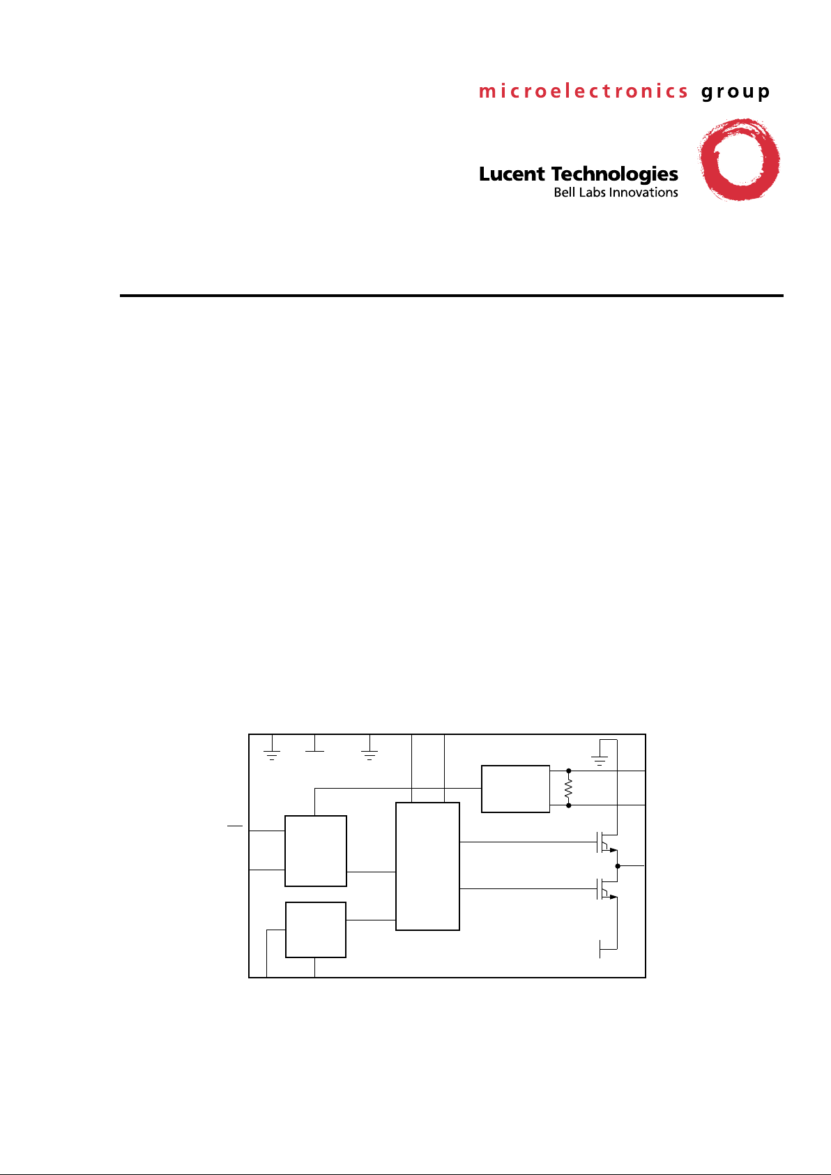
The L7590C Telephone Ringing Driver produces a
low-frequency sinusoidal ringing signal for analog
telephone loops. This is accomplished by producing
an output pulse stream that is an amplified replica of
the digital input. The output is then filtered to produce
a sine wave. The peak-to-peak output level is determined by the magnitude of the negative high-voltage
dc applied to the device (up to –170 V).
The required input is a 100 kHz CMOS-compatible
pulse stream, pulse-width modulated (PWM) at the
desired ringing frequency. The output stage consists
of one upper and one lower drive transistor with an
internal control circuit.
The L7590C IC is optimized for low po wer dissipation
and is available in a 16-pin, surface-mount package.
12-3057a (f)
Figure 1. Block Diagram
CLOCK
CONTROL
LEVEL
SHIFT
AND
OUTPUT
TIMING
CURRENT
LIMIT
BIAS
CIRCUIT
OUT
GNDD
V
DD
CLK
V
REF
VNEG
GNDR
CB1 CB2
EN
30 Ω
L1
L2
VNEG
Page 2
2 Lucent Technologies Inc.
Data Sheet
June 1998
L7590C Telephone Ringing Driver
Pin Information
Absolute Maximum Ratings
(T
A
= 25 ° C)
Stresses in excess of the absolute maximum ratings can cause permanent damage to the device. These are absolute stress ratings only. Functional operation of the device is not implied at these or any other conditions in excess
of those given in the operational sections of this data sheet. Exposure to absolute maximum ratings for extended
periods may adversely affect device reliability.
Pin Symbol Type Name/Function
14 V
DD
—
+5 V Power Supply .
3 GNDD — Digital Ground .
12 GNDR — Ringing Ground .
8V
NEG
—
Negative Power Supply . Determines the swing of the ringing generator. Connect
a 1 µ F capacitor from V
NEG
to V
REF
.
5V
REF
—
Internal Reference Voltage . Connect a 1 µ F capacitor from V
REF
to V
NEG
.
16 CLK I
Clock . Modulated pulse stream. Low = 0 V. High = V
DD
.
7 OUT O Ringing Generator Output . Connect to ringing relay contact through a filter.
1 CB1 — Bootstrap Capacitor . Connect a 0.1 µ F capacitor between CB1 and CB2.
2 CB2 — Bootstrap Capacitor . Connect a 0.1 µ F capacitor between CB1 and CB2.
9L1—
Filter Inductor . Connect an inductor to pin L2.
10 L2 — Filter Inductor . Connect an inductor to pin L1.
15
EN
—
Not Enable . A logic lo w activates the internal circuitry. A logic high puts the device
in a low-power powerdown mode.
Parameter Min Typ Max Unit
V
DD
— 7.0 — V
V
NEG
— –200 — V
Timing Input Voltage –0.5 — 7.0 V
Storage Temperature Range –40 — 125
°
C
Maximum Junction Temperature — 150 —
°
C
Relative Humidity Range 5 — 95 %
Page 3
Lucent Technologies Inc. 3
Data Sheet
June 1998
L7590C Telephone Ringing Driver
Recommended Operating Conditions
Electrical Characteristics
Electrical characteristics apply for 25 ° C. Unless noted, V
DD
= +5 V, V
NEG
= –170 V,
EN
= low, L1 = 20 mH
(Rdc = 20 Ω , Ceff = 20 pF), CLK = 100 kHz. Positive currents flow into the device. Typical is defined as 25 ° C.
Parameter Min Typ Max Unit
Ambient Temperature –40 — 85
°
C
V
DD
Supply Voltage 4.75 5.0 5.25 V
V
NEG
Supply V oltage –170 — –130 V
Parameter Min T yp Max Unit
Power Supply—Idle (CLK = H or L,
EN
= high, dc):
I
DD
I
NEG
Power Dissipation
—
—
—
—
—
—
1
–50
13.5
mA
µ
A
mW
Power Supply—Active, No Load:
I
DD
I
NEG
Power Dissipation
—
—
—
—
–3.2
—
3
–8
1.38
mA
mA
W
Efficiency =
{[
(V
OUT
)
2
/R
LOAD
]/(V
NEG
•
I
NEG
)
}
:
Sinking Current, R
LOAD
= 1400 Ω Load to GND
Sourcing Current, R
LOAD
= 1400 Ω Load to V
NEG
40
40
80
80
—
—
%
%
ON-resistance:
CLK = H, I
OUT
= –20 mA
CLK = L, I
OUT
= +20 mA
0
0
10
10
20
20
Ω
Ω
Current Limit 25 — 40 mApeak
Page 4

44 Lucent Technologies Inc.
Data Sheet
June 1998
L7590C Telephone Ringing Driver
Functional Description
Ringer Requirements
This discussion highlights some of the requirements in
the United States and Germany. Beginning with the
telephone set ringer to be powered, the United States
requires 40 Vrms to be delivered to the equivalent of
five parallel telephone sets, or 5 REN (Ringer Equivalence Number), that translates to 1386 Ω + 40 µ F. In
Germany , 30 mApeak must be deliv ered to f our parallel
telephone sets. In Germany, 4 REN have an impedance of 450 Ω + 3.4 µ F. The difference results from the
impedance of the telephone-set ringers of the two
countries.
Ringing Requirements
In Germany, both single-ended ringing and balanced
ringing can be used. This is not so in the United States,
where some ringers on older equipment have a ground
connection at the telephone set, and the signal lead is
either the Tip or Ring wire of the twisted pair. This has
led to the recommended use of single-ended ringing.
Both administrations allow ringing with a negative dc
level, known as battery-backed ringing, but in the
United States, there is a constraint that this level cannot be more negative than –75 V.
With the exception of the United States, most worldwide administrations require an injection of a pure sine
wave. Depending on the country, the distortion requirement is in the range of 3% to 5%. In the United States,
the wave does not need to resemb le a sine w a ve, but it
cannot be a square wave. The shape requirement of
the wave in the United States is expressed as a crest
factor (c.f.). This is the ratio of the peak to the rms voltage of the signal. The requirement is 1.2 < c.f. < 1.6.
Operation
On the L7590C, the prefiltered output is a highvoltage replica of the PWM digital signal that is applied
to the CLK input. The signal at OUT is produced by
level shifting and control of the high-v oltage transistors .
The level is determined by the magnitude of the negative dc voltage applied to the output stage transistors.
The output, ideally, should be an exact time replica of
the CLK input to faithfully reproduce the modulating
waveform. This high-voltage replica of the CLK input is
filtered to leave only the low-frequency, high-voltage
sine wave ringing signal. Figure 3, parts A and B, illustrates the PWM signal with relation to the modulating
signal frequency. The PWM signal is at a 100 kHz rate
and modulated at the desired ringing signal frequency,
typically 20 Hz to 30 Hz. Laboratory equipment generation of the required signal is shown in Figure 5. Propagation delays and switching parameters associated
with the control circuitry and output stage transistors
can cause skewing which will produce a distorted output of the modulating waveform. Skewing is illustrated
in Figure 4, parts A, B, and C. The skewing can be
seen as an increase in the duty cycle of the L7590C
output compared to the input signal duty cycle.
Using the test arrangement as shown in Figure 5, the
harmonic distortion of the filtered output of the L7590C
was measured with two different loading circuits. With
the North American 5 REN (1386 Ω + 40 µ F) load, the
THD was typically 2.0% to 2.5%. With the Germany
4 REN (450 Ω + 3.4 µ F) load, the THD was typically
1.5% to 2.0%. The 25 Hz output of the
HP
* 3311A
generator showed a typical THD of 1.5% when supplying a signal to the
HP
8116A.
A 20 Ω resistor (R
ILIM
) must be added between L1 and
OUT for 5 REN loads.
*
HP
is a registered trademark of Hewlett-Packard Company.
Page 5

Lucent Technologies Inc. 5
Data Sheet
June 1998
L7590C Telephone Ringing Driver
Application
* C
NEG
connects to V
NEG
pin at chip.
12-3058.E (F)
Figure 2. Basic Battery-Backed Ringing Application
Table 1. Parts List for Application, Ringing Driver IC
Name Value Function
L1 20 mH Part of LC output filter
C1 1 µ F, 250 V, 20% Part of LC output filter
C2 1 µ F, 20 V, 20% V
REF
filter
CB 0.1 µ F, 10 V, 20% Voltage doubling capacitor
Rx 15 Ω , 1 W Hot insertion limiter
R
ILIM
20 Ω to 100 Ω Current-limiter adjustment
VDD GNDD
V
REF
VNEG
CLK
OUT
TIP
RP
20 Ω
RING
L7581
RELAY
PWM
SIGNAL
C1
1.0 µF
V
DD
L7590C
RINGING
GENERATOR
C2
1 µF
R
TS1
400 Ω
250 V PROT
PT
PR
RING TRIP
DETECT
SLIC
XMT
RCV
CODEC
RP
20 Ω
VNEG
L2
L1
L1
20 mH
GNDR
CB
0.1 µF
CB1 CB2
EN
RILIM
RX 15 Ω
DX
DR
CNEG*
1.0 µF
Page 6

6 Lucent Technologies Inc.
Data Sheet
June 1998
L7590C Telephone Ringing Driver
Application (continued)
12-3381 (F)
12-3380 (F)
B. Same as A but Expanded
A. Upper = PWM Signal Centered at 100 kHz
Lower = Modulating Signal
Figure 3. Modulation Waveforms
Page 7

Data Sheet
June 1998
Lucent Technologies Inc. 7
L7590C Telephone Ringing Driver
Application (continued)
12-3379 (F) 12-3377 (F)
B. 50% Duty Cycle
A. Upper = 10% Duty Cycle—CLK Input
Lower = L7590C Output
12-3376 (F)
C. 90% Duty Cycle
Note: For all three illustrations above, the positive portion of the L7590C output is skewed to be greater than the CLK input.
Figure 4. Skewing Illustration Waveforms
Page 8

8 Lucent Technologies Inc.
Data Sheet
June 1998
L7590C Telephone Ringing Driver
Application (continued)
12-3375.B(F)
Notes:
THD % =
x 100.
RX = 15 Ω.
Figure 5. L7590C Test Connections
HP
3311A
SIGNAL
GENERATOR
25 Hz
+5 V
0.1 µF
100 kHz (PWM)
SIGNAL LEVEL = 0 V TO 5 V
PULSE/FUNCTION
GENERATOR
100 kHz RATE
HP
8116A
VDD CB1 CB2GNDD
OUT
L1
GNDR
L2
RILIM
20 mH
C1
1.0 µF
450 Ω
3.4 µF
1386 Ω
40 µF
HP
3585A
SPECTRUM
ANALYZER
V
NEG = –170 V
RX
C2
1 µF
CLK
EN
VNEGVREF
L7590C
CNEG
1.0 µF
E22E32E42. . .+++
E1
2E22E32E42
. . .++++
----------------------------------------------------------------------------------
Page 9

Lucent Technologies Inc. 9
Data Sheet
June 1998
L7590C Telephone Ringing Driver
Outline Diagram
16-Pin, Plastic SOG
Dimensions are in millimeters.
5-4414r2 (C)
Number
of Pins
(N)
Maximum
Length
(L)
Maximum Width
Without Leads
(B)
Maximum Width
Including Leads
(W)
Maximum Height
Above Board
(H)
16 10.49 7.62 10.64 2.67
W
0.61
0.51 MAX
H
0.28 MAX
0.10
SEATING PLANE
1.27 TYP
N
L
B
1
PIN #1 IDENTIFIER ZONE
Page 10

Data Sheet
June 1998
L7590C Telephone Ringing Driver
Lucent Technologies Inc. reserves the right to make changes to the product(s) or information contained herein without notice. No liability is assumed as a result of their use or application. No
rights under any patent accompany the sale of any such product(s) or information.
Copyright © 1998 Lucent Technologies Inc.
All Rights Reserved
June 1998
DS98-340ALC (Replaces DS97-512ALC)
For additional information, contact your Microelectronics Group Account Manager or the following:
INTERNET: http://www.lucent.com/micro
E-MAIL: docmaster@micro.lucent.com
N. AMERICA: Microelectronics Group, Lucent Technologies Inc., 555 Union Boulevard, Room 30L-15P-BA, Allentown, PA 18103
1-800-372-2447, FAX 610-712-4106 (In CANADA: 1-800-553-2448, FAX 610-712-4106)
ASIA PACIFIC:Microelectronics Group, Lucent Technologies Singapore Pte. Ltd., 77 Science Park Drive, #03-18 Cintech III, Singapore 118256
Tel. (65) 778 8833, FAX (65) 777 7495
CHINA: Microelectronics Group, Lucent Technologies (China) Co., Ltd., A-F2, 23/F, Zao Fong Universe Building, 1800 Zhong Shan Xi Road,
Shanghai 200233 P. R. China
Tel. (86) 21 6440 0468, ext. 316, FAX (86) 21 6440 0652
JAPAN: Microelectronics Group, Lucent Technologies Japan Ltd., 7-18, Higashi-Gotanda 2-chome, Shinagawa-ku, Tokyo 141, Japan
Tel. (81) 3 5421 1600, FAX (81) 3 5421 1700
EUROPE: Data Requests: MICROELECTRONICS GROUP DATALINE: Tel. (44) 1189 324 299, FAX (44) 1189 328 148
Technical Inquiries:GERMANY: (49) 89 95086 0 (Munich), UNITED KINGDOM: (44) 1344 865 900 (Bracknell),
FRANCE: (33) 1 48 83 68 00 (Paris), SWEDEN: (46) 8 600 7070 (Stockholm), FINLAND: (358) 9 4354 2800 (Helsinki),
ITALY: (39) 2 6608131 (Milan), SPAIN: (34) 1 807 1441 (Madrid)
Ordering Information
Device Part No. Description Package Comcode
LUCL7590CAE-D Telephone Ringing Driver 16-Pin SOG 108191107
LUCL7590CAE-DT Telephone Ringing Driver 16-Pin SOG (Tape and Reel) 108191115
 Loading...