

Page 1
In the absence of confirmation by device specification sheets, SHARP takes no responsibility for any defects that may occur in equipment using any SHARP devices shown in
catalogs, data books, etc. Contact SHARP in order to obtain the latest device specification sheets before using any SHARP device.
1
DESCRIPTION
The LU850425 is a CMOS 8-bit single-chip
microcomputer for CCD digital camera systems
which include a CDS/AGC IC (IR3Y38M), a DSP
IC (LR38266), a timing generator IC (LR38578),
and this microcomputer IC.
FEATURES
• Auto exposure control (electronic exposure and
mechanical exposure)
• Auto carrier balance tuning
• Auto white balance control
• In combination with an external controller
(personal computer), functions below can be
controlled (see "Serial Control Interface" in
FUNCTIONAL DESCRIPTION)
q Switchable :
AGC/ON/OFF
Auto white balance/AUTO/PRESET
Aperture enhancement/ON/OFF
Back light compensation/ON/OFF
GAMMA correction/ON/OFF
w Electronic shutter speed selection :
Auto E/E [1/60 (1/50) to 1/70 000 s] or fixed E/E
[1/60 (1/50), 1/100 (1/60), 1/250, 1/500, 1/1 000,
1/5 000 and 1/10 000 s]
( ) = PAL mode
• Switchable between NTSC and PAL modes
• Single +3.3 V power supply
• Package :
100-pin LQFP (LQFP100-P-1414) 0.5 mm pin-pitch
LU850425
LU850425
8-bit Microcomputer for
DSP Camera Systems
Page 2

LU850425
2
PIN CONNECTIONS
1
2
3
4
5
6
7
8
9
10
11
12
13
14
15
16
17
18
19
20
21
22
23
24
25
GND
CDS SEL
TV MODE
MODEL
LENS SEL
ADJIN
AGC SEL
ABLC
IRIS
GAMMA
UIN
UOUT
READY
GND
SOUT
SCK
SLDI
TIM SEL
DATA
0
DATA1
DATA2
DATA3
DATA4
DATA5
DATA6
75
74
73
72
71
70
69
68
67
66
65
64
63
62
61
60
59
58
57
56
55
54
53
52
51
GND
EESRB
EEDATA
EECLK
GND
MCO
GND
GND
GND
GND
VD
GND
DAV
R1
DAVR0
VREF OUT
IRIS OUT
GND
IRISSEL
3
IRISSEL2
IRISSEL1
VR
B-Y
R-Y
GND
GND
26272829303132333435363738394041424344454647484950
DATA7
ADD0
ADD1
ADD2
ADD3
ADD4
ADD5
ADD6
NC
NC
XCK
2
XCK1
GND
NCNCNC
NC
DACK
DADT
DASTB
AGND
SPD
WB
IWIND
GND
100
9998979695949392919089888786858483828180797877
76
GND
APT
MIR SET
WBSEL3WBSEL2
WBSEL1NCAEAWB LOCK
ROMDATA
ROMCLK
TEST
VDDGND
OSCINOSCOUT
RESET
GND
GND
GND
GND
GND
GND
SDATA
SCK
NC
100-PIN LQFP
TOP VIEW
(LQFP100-P-1414)
Page 3
3
PIN DESCRIPTION
LU850425
–
–
–
–
–
–
–
–
–
–
–
–
–
–
–
–
–
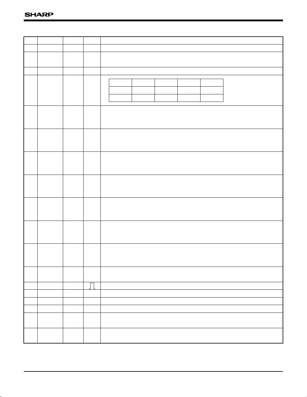
PIN NO.
SYMBOL
POLARITY
I/O DESCRIPTION
1 GND I A grounding pin.
2 CDS SEL I
CDS/AGC IC selection.
When using IR3Y38M, set to H level.
TV standard/CCD selection.I
I
TV MODE
MODEL
3
4
6
Adjustment selection.
H : Camera
L : Adjustment
ADJIN I
5
Selection of output of pin 60 (pin 9 is input H level).
H : Auto exposure lens
L : Passive exposure lens
LENS
SEL
I
IABLC
Selection of auto backlight compensation.
L : ABLC OFF
H : ABLC ON
8
I
AGC SEL
Selection of AGC function.
H:ON
L : OFF
7
IIRIS
Exposure mode selection.
H : Mechanical exposure
L : Electronic exposure
9
10
Selection of gamma correction.
H : ‹ = 1.0
L : ‹ = 0.45
GAMMA I
OUOUT
Outputs the serial data to adjustment tool or PC.
For details, see "Serial Control Interface" in FUNCTIONAL DESCRIPTION.
12
IUIN
The serial data is fed from adjustment tool or PC.
Without input data, keep at H level.
For details, see "Serial Control Interface" in FUNCTIONAL DESCRIPTION.
11
13 Outputs high level at AE/AWB lock mode.READY O
IGND A grounding pin.14
16 Outputs the clock signal to LR38266.SCK O
15 Outputs the serial data to LR38266.SOUT O
OSLDI
Outputs the strobe signal to LR38266. LR38266 latches the serial data from
pin 15 of LU850425 by both SCK and SLDI.
17
HLPin 3
Pin 4 L LH
H
H
L
270 k 320 kCCD 470 k410 k
18
Timing IC selection.
When using LR38578, set to H level.
TIM SEL I
Page 4

4
LU850425
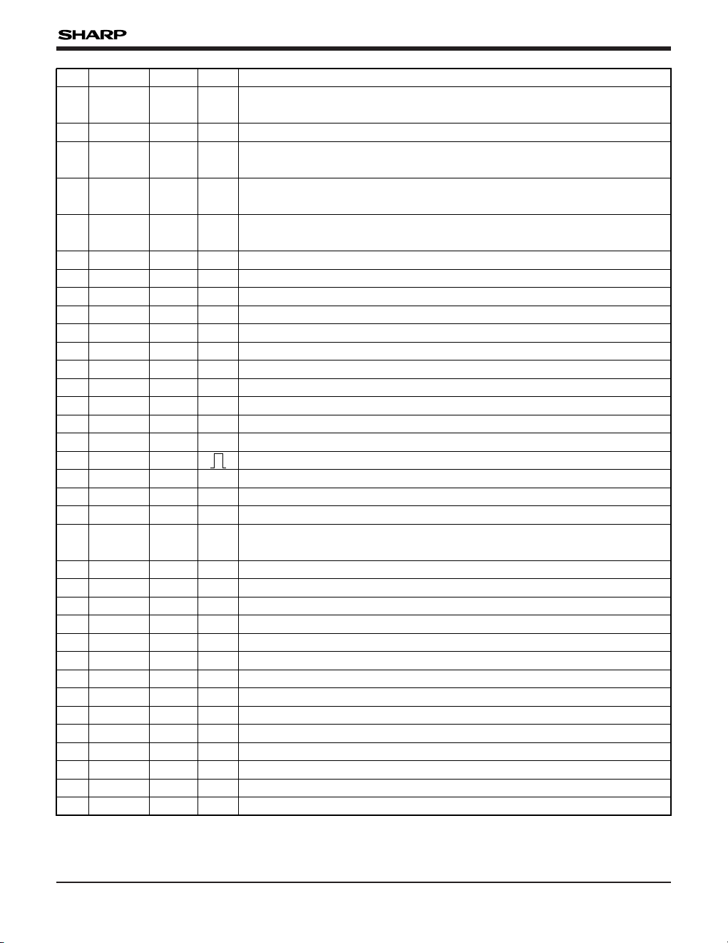
PIN NO.
SYMBOL
POLARITY
I/O DESCRIPTION
19 DATA
0 I
–
–
IDATA625
–
IDATA524
–
IDATA423
–
IDATA322
–
IDATA221
–
IDATA120
26 DATA
7 I
–
Inputs image data from LR38266.
DATA
0 : LSB
DATA
7 : MSB
Outputs address data to LR38266.
ADD
0 : LSB
ADD6 : MSB
Master clock output.
–
OXCK236
No connection.
–
ONC35
No connection.
–
ONC34
–
OADD633
–
OADD532
–
OADD431
–
OADD330
–
OADD229
–
OADD128
–
OADD027
43 DACK O
–
Outputs the clock signal to MB88346BV. For details, see "TIMING CHART (D)".
42 NC O
–
No connection.
41 NC O
–
No connection.
40 NC O
–
No connection.
39 NC O
–
No connection.
38 GND –
–
A grounding pin.
37 XCK
1 I
–
Master clock input (5.5 MHz, TYP.).
Outputs the strobe signal to MB88346BV. For details, see "TIMING CHART (D)".
–
ODASTB45
Outputs the serial data to MB88346BV. For details, see "TIMING CHART (D)".
–
ODADT44
A grounding pin for D/A output circuit.
–
–AGND46
47 SPD I
–
Inputs DC level to select shutter speed. For details, see "
ELECTRONIC
SHUTTER SPEED CONTROL
" in Preset Function Control.
Inputs DC level to select white balance mode. For details, see "
WHITE
BALANCE
" in Preset Function Control.
–
IWB48
Inputs DC level to select exposure window. For details, see "
(3) Window
Selection of Emphasis Range at Auto Exposure
" in ELECTRONIC SHUTTER
SPEED CONTROL.
–
IIWIND49
50 GND I
–
Not used. A grounding pin.
Not used. A grounding pin.
IGND51
Not used. A grounding pin.
–
IGND52
53 R – Y I
–
Inputs DC level to vary R – Y gain by manual. The detail is shown at "WHITE
BALANCE" in Preset Function Control.
Page 5
5
LU850425
PIN NO.
SYMBOL
POLARITY
I/O DESCRIPTION
Inputs the reference DC voltage for built-in A/D.
–
IVR55
A grounding pin.
–
IGND59
54 B – Y I
–
Inputs DC level to vary B – Y gain by manual. The detail is shown at "WHITE
BALANCE" in Preset Function Control.
56 IRISSEL
1 I
–
Inputs the preset shutter speed mode 1. (See
"ELECTRONIC SHUTTER SPEED
CONTROL"
in Preset Function Control.)
Inputs the preset shutter speed mode 3. (See
"ELECTRONIC SHUTTER SPEED
CONTROL"
in Preset Function Control.)
–
IIRISSEL358
Inputs the preset shutter speed mode 2. (See
"ELECTRONIC SHUTTER SPEED
CONTROL"
in Preset Function Control.)
–
IIRISSEL257
60 IRIS OUT O
–
Outputs the analog signal to control auto mechanical exposure lens.
Inputs DC reference voltage for built-in D/A output of pin 60.
–
IDAVR062
Outputs the VREF DC to IR3Y38M.
–
O
V
REF
OUT
61
64 GND I
–
Not used. A grounding pin.
63 DAV
R1 I
–
Inputs DC reference voltage for built-in D/A output of pin 61.
A grounding pin.
–
IGND66
Inputs VD signal from LR38266.
–
IVD65
Outputs the clock signal to LR38578.
–
OEECLK72
A grounding pin.
–
IGND71
Inputs MCO signal from LR38266.
IMCO70
A grounding pin.
–
IGND69
A grounding pin.
–
IGND68
A grounding pin.
–
IGND67
Outputs the data signal to LR38578.
–
OEEDATA73
74 EESRB O
–
Outputs the strobe signal to LR38578. This signal makes LR38578 latch the
data of EEDATA (pin 73) by EECLK (pin 72).
75 GND –
–
A grounding pin.
Outputs the clock signal to CDS/AGC (IR3Y38M).
–
OSCK77
No connection.
–
ONC76
A grounding pin.
–
IGND84
A grounding pin.
–
IGND83
A grounding pin.
–
IGND82
A grounding pin.
–
IGND81
A grounding pin.
–
IGND80
A grounding pin.
–
–GND79
Outputs the serial data to CDS/AGC (IR3Y38M).
–
OSDATA78
86 OSC
OUT O
–
No connection.
85 RESET I
–
Inputs the reset signal of LU850425.
A grounding pin.
–
–GND88
A grounding pin.
–
IOSCIN87
Page 6

6
LU850425
PIN NO.
SYMBOL
POLARITY
I/O DESCRIPTION
91 ROMCLK O
–
Outputs the clock to EEPROM.
For details, see "TIMING CHART (A)".
90 TEST –
–
Connected to GND.
89 V
DD I
–
Supply of +3.3 V power.
AE and AWB lock selection.
H : Auto exposure, auto white balance lock ON
L : Auto exposure, auto white balance lock OFF
–
I
AEAWB LOCK
93
Inputs the data from EEPROM/output the data to EEPROM. For details, see
"TIMING CHART (A)".
–
I/O
ROMDATA
92
94 NC O
–
No connection.
White balance mode selection.
For details, see "WHITE BALANCE" in Preset Function Control.
–
IWBSEL195
98 MIR SEL I
–
Mirror mode selection.
L : Normal mode
H : Mirror mode
97 WBSEL
3 I
–
White balance mode selection.
For details, see "WHITE BALANCE" in Preset Function Control.
96 WBSEL
2 I
–
White balance mode selection.
For details, see "WHITE BALANCE" in Preset Function Control.
99 APT I
–
Selection of aperture enhancement.
H:ON
L : OFF
A grounding pin.
–
IGND100
Page 7

LU850425
7
Start
Bit
D0 D1 D2 D3 D4 D5 D6 D7
Even
Parity
Bit
Stop
Bit
UIN
GND
MSBLSB
3.3 V
Data Bit
UIN
Micro-
computer
PC or
Adjustment tool
UOUT
UIN
UOUT
T
XD
R
XD
FUNCTIONAL DESCRIPTION
Serial Control Interface
(For adjustment tool)
FORMAT OF DATA TRANSFERS
• Format of transfers : Asynchronous (Based on
RS-232C standard)
• Bit rate : 9 600 bps
• Data length : 8 bits
• Parity check : 1 even parity bit
• Start bit : 1 bit
• Stop bit : 1 bit
• Signal voltage level (CMOS)
ADJUSTMENT MODE
When the signal level of pin 6 (ADJIN) is low, the
video quality adjustment by a PC or an adjustment
tool is possible.
When the signal level of pin 6 (ADJIN) is high, the
microcomputer control is by a PC.
• Connection
Page 8

LU850425
8
Preset Function Control
(by high/low condition at inputs and by DC level of
A/D inputs)
Below functions are available to be selected under
the condition of a low level of pin 6 (ADJIN).
WHITE BALANCE
(1) White Balance Mode Selection by Pins 95, 96
and 97 (Digital Input)
White balance mode is selected by the combination
of high/low level at three pins below.
(2) White Balance Mode Selection by Pin 48
(Analog Input)
White balance mode can be selected by DC input
level at pin 48 if all the above 95, 96, and 97 pins
are connected to low.
WBSEL1
95 PIN
WBSEL2
96 PIN
LL L
WBSEL3
97 PIN
WHITE BALANCE MODE NOTE
A/D input (pin 48) control is available. See "(2) White
Balance Mode Selection by Pin 48 (Analog Input)".
A/D input (pin 53 and 54) control is available.LLH
HH H 1Preset mode 4
LHH 1Preset mode 3
HL H 1Preset mode 2
LLH 1Preset mode 1
H H L Auto white balance mode.
L H L Set the condition just before selecting this mode.
VOLTAGE LEVEL (PIN 48)
0 to 0.47 V
WHITE BALANCE MODE NOTE
Auto white balance.
Preset mode 4 12.83 to 3.3 V
Preset mode 3 12.36 to 2.82 V
Preset mode 2 11.89 to 2.35 V
Preset mode 1 11.42 to 1.88 V
Analog input (pins 53 and 54) control is available.0.95 to 1.41 V
Set the condition just before feed this DC level.0.48 to 0.94 V
NOTE :
1. All of above preset modes are optional and each mode should be adjusted by a PC or an adjustment tool.
Page 9

9
LU850425
ELECTRONIC SHUTTER SPEED CONTROL
(1) Electronic Shutter Speed Selection by Pins 56,
57 and 58 (Digital Input)
An electronic shutter speed can be selected by the
combination of high/low level at three pins below
under the condition of a high level of pin 9 (IRIS).
(2) Electronic Shutter Speed Selection by Pin 47
(A/D Input)
An electronic shutter speed can be selected by DC
input level of pin 47 if all the above 56, 57 and 58
pins are connected to low.
IRISSEL1
(PIN 56)
IRISSEL
2
(PIN 57)
LL L
IRISSEL
3
(PIN 58)
SHUTTER SPEED NOTE
A/D input (pin 47) control is available. See "(2) Electronic
Shutter Speed Selection by Pin 47 (A/D Input)".
1/60 s (NTSC), 1/50 s (PAL)LLH
HH H 1Preset mode 5
LHH 1Preset mode 4
HL H 1Preset mode 3
LLH 1Preset mode 2
HH L 1Preset mode 1
L H L 1/100 s (NTSC), 1/60 s (PAL) (flicker-less mode)
VOLTAGE LEVEL (PIN 47)
0 to 0.41 V
SHUTTER SPEED NOTE
1/60 s (NTSC), 1/50 s (PAL)
Preset mode 5 12.46 to 2.87 V
Preset mode 4 12.06 to 2.45 V
Preset mode 3 11.65 to 2.05 V
Preset mode 2 11.24 to 1.64 V
Preset mode 1 10.83 to 1.23 V
1/100 s (NTSC), 1/60 s (PAL)0.42 to 0.82 V
NOTE :
1. All of above preset modes are optional and each mode should be adjusted by a PC or an adjustment tool.
2.88 to 3.3 V 1Preset mode 6
Page 10

LU850425
10
Auto Exposure Control
• Auto exposure control has the following three
functions :
q E/E (Electronic Exposure) function
w Mechanical exposure function
e AGC (Automatic Gain Control) function
Carrier Balance Control
• Carrier balance control has the following two
functions.
q At power on, carrier balance is automatically
tuned.
w Carrier balance is automatically tuned against
AGC operation.
Auto White Balance Control
• Control method : A white color temperature
control is sampled by an I/Q conversion signal.
• By the reasoning of the video condition from I/Q,
brightness, and other signal levels, white balance
is controlled to keep the best condition.
(3) Window Selection of Emphasis Range at Auto Exposure
INPUT VOLTAGE (PIN 49)
0 to 0.8 V
RANGE SELECTION
Preset 1 See "Fig. 1".
Whole range2.41 to 3.3 V
Preset 3 See "Fig. 1".
1.61 to 2.4 V
Preset 2 See "Fig. 1".0.81 to 1.6 V
A
A
B
C
A
B
C
A
B
C
A = 25% B = C = 100% Emphasis range
Preset 1 Preset 2 Preset 3
A
AA
Fig. 1 Emphasis Range
Page 11

LU850425
11
TIMING CHART
(A) LU850425 (µCOM),/BF24C04F (EEPROM)
1. Write Mode (Writing data that is sent from the adjustment tool to the EEPROM.)
2. Read Mode
5.5 µs
RMDA
RMCK
Chip Address
ACK
ACKACK
Word Address Write Address
WA7
D7 D6
Start
Stop
11 µs
1100 0000
12.5 µs
88 µs 5 µs
WA0
D0
WA6
ACK
ACK
Read Data
[Address 0
EPROM data]
Word
Address
11 µs 11 µs
11 µs
11 100000
11 µs
29 µs
88 µs
Chip Address Chip Address
Start
D
7 D0
1100 0000
RMDA
RMCK
WA0WA7
ACK
ACK ACK
ACK
Read
Data Read Data
D7 D7D0 D0
11 µs
RMDA
RMCK
Stop
[Address 1
EPROM data]
[Address 255
EPROM data]
EEPROM MARK MINIMUM (µs)
t
SU : STO 11
t
SU : STA 11
tHD : STA 11
t
LOW 88
t
HIGH 11
Page 12

LU850425
12
(B) LU850425 (µCOM),/LR38266 (DSP)
(C) LU850425 (µCOM),/IR3Y38M (CDS/AGC)
SCK
SOUT
SLDI
DSP Address (18h) DSP Data (26h)
A
7 A6 A5 A4 A3 A2 A1 A0 D7 D6 D5 D4 D3 D2 D1 D0
1.4 µs
5.6 µs
11.6 µs
D9
SCK
SDATA
D
8 D7 D6 D5 D4 D3 D2 D1 D0
1.5 µs 8.6 µs 3 µs 2.7 µs 4.3 µs
Latch
(D) LU850425 (µCOM),/LR38578 (TIMING GENERATOR IC)
EECLK
EEDATA
EESRB
D
0
D2
D1 D5 D6 D7 D8
SMD
1
SMD2MR1MR
2
MC
1
MC2MS1MS
2
MF
2MF1
LatchD3 D4
1.5 µs
1.5 µs
1.5 µs
6 µs
(E) LU850425 (µCOM),/MB88346BV (D/A)
Analog voltage is suited
to data (64h)
(MB88346BV pin 4)
11 11000 10000
Address (0Ah)
Data (64h)
3.0 µs
15.5 µs 9.5 µs
3.5 µs
3.0 µs
10.5 µs
3.5 µs
DACK
DATA
A05
DAST
(Ex.)
Page 13

13
Total output current ÇIOH –20 mA 3HIGH level
Output "High" current I
OH –4 mA 3
LU850425
Power supply voltage VDD –0.3 to +6.5 V
PARAMETER SYMBOL RATING NOTEUNIT
V–0.3 to V
DD + 0.3VOOutput voltage
V–0.3 to VDD + 0.3VIInput voltage
1mA+30I
OL1
Output "Low" current
I
OL2 +4 mA 2
LOW level
1mA+100ÇI
OL1
Total output current
ÇI
OL2 +20 mA 2
Operating temperature T
OPR –10 to +50 ˚C
˚C–50 to +150T
STGStorage temperature
ABSOLUTE MAXIMUM RATINGS
Power supply voltage VDD 2.7 3.6 V
PARAMETER SYMBOL MIN. UNITMAX.
RECOMMENDED OPERATING CONDITIONS
OSCILLATION CIRCUIT (EXAMPLE)
*
* Don't put any signal line cross the oscillation circuit line.
NOTES :
1. Applied to outputs. (Pins 27 to 34 and 39 to 45 without input pin.)
2. Applied to outputs. (Except pins 27 to 34 and 39 to 45 without input pin.)
3. Applied to all outputs.
TYP.
3.3
5.5 MHz5.755.25f
CKSystem clock frequency
CK1
CK2 GND
Ceramic OSC
C1 C2
Oscillation frequency resistor is contained
within the IC. (Recommendation)
Ceramic oscillator = PBRC5.50B
(KYOTO CERAMIC CO. LTD.)
(PBRC5.50B is contained C
1, C2.)
Page 14

IOH = –0.6 mA, VDD = 3 V
V
DD
– 0.5
VOH2
IOH = –0.6 mA, VDD = 3 V
V
DD
– 0.5
VOH1
IIH1 10VIN = VDD, VDD = 3 V
VV
DD
V
DD
– 0.3
VIH2
VIH1 0.8VDD VDD
LU850425
14
ELECTRICAL CHARACTERISTICS
DC Characteristics
(VDD = 2.7 to 3.3 V, TOPR = –20 to +70 ˚C)
Input voltage
PARAMETER SYMBOL CONDITIONS MIN. TYP. MAX.VUNIT NOTE
1
2
V
V
0.2V
DD
0.3
0
0
V
IL1
VIL2
IIL2 –10 –25 –50VIN = 0 V, VDD = 3 V µA 4
I
IL1 –10VIH = 0 V, VDD = 3 V
µA
µA
3
Input current
LSB
V
R = VDD = 3 V,
f
M = 5.5 MHz
±6±4
LSB
V
R = VDD = 3 V,
fM = 5.5 MHz
±2.5±1
bits
V
R = VDD = 3 V,
fM = 5.5 MHz
10
±3 ±5
V
R = VDD = 3 V,
f
M = 5.5 MHz
LSB
A/D
Resolution
Differential linear tolerance
Linear tolerance
Combined tolerance
6
V
V
I
OL = 6 mA, VDD = 3 V 1VOL1
5
V
V
OL2 0.5IOL = 0.6 mA, VDD = 3 V
V
Output voltage
Combined tolerance ±0.03 ±0.06 V
Output resistance 6 k$
Resolution 8V
R = VDD = 3 V bits
7D/A
9µA
f
SUB oscillation,
STOP mode
4020
8
mAf
SYS = 2.25 MHz 84
I
DDS1
IDDH
IDD
IDDS2
Power consumption
f
SYS = 2.25 MHz,
HALT mode
f
SUB stop,
STOP mode
1
1
2
6
mA
µA 10
NOTES :
1. Applicable pins : 95 to 100, 1, 81 to 84, 91 to 94, 64 to
66, 47 to 54, 19 to 26, 12, 13, 15, 17, 18, 72 to 75, 77
to 80 without output pin.
2. Applicable pins : RESET, 3 to 10, 67 to 71, 11, 14, 16,
XCK
1 without output pin.
3. Applicable pins : 3 to 10, 95 to 100, 1, 81 to 84, 91 to
94, 64 to 71, 47 to 54, 19 to 26, 11 to 18, 72 to 75, 56
to 59 without output pin.
4. Applicable pin : RESET
5. Applicable pins : 27 to 34, 35, 39 to 45 without input pin.
6. Applicable pins : 95 to 100, 1, 81 to 84, 91 to 94, 64 to
71, 19 to 26, 11 to 15, 72 to 75, 77 to 80, 56 to 59
without input pin.
7. Applicable pins : 60, 61
8. No load condition, V
DD = 3 V, main-clock frequency =
5.5 MHz
9. No load condition, V
DD = 3 V, fSUB oscillation status
(32.768 kHz), V
R = GND, input signal fixed.
10. No load condition, V
DD = 3 V, OSCIN = GND, VR =
GND, input signal fixed.
Page 15

PACKAGES FOR CCD AND CMOS DEVICES
15
Unit : mm
0.1
±0.1
Package
base plane
1
0.125
±0.05
0.2
±0.08
0.5
TYP.
25
26
50
5175
76
100
14.0
±0.2
14.0
±0.2
16.0
±0.3
1.4
±0.2
0.6375
15.0
±0.2
(1.0)
(1.0)
(1.0)
(1.0)
0.08
0.1
M
16.0
±0.3
1.70
MAX.
100 LQFP (LQFP100-P-1414)
PACKAGE (Unit : mm)
 Loading...