

Page 1

Data Sheet
July 2000
LU6612
for 10Base-T/100Base-TX
FASTCAT
TM
Single-FET
Features
10 Mbits/s Transceiver
■
Compatib le wit h
for twisted-pair cable
■
Autopolarity detection and correction
■
Adjustable squelch level for extended wire line
length capability (2 levels)
■
Interfaces with
interface (MII)
■
On-chip filtering eliminates the need for external filters
■
Half- and full-duplex operations
100 Mbits/s Transceiver
■
Compatib le w ith
(clause 23), PMA (clause 24), autonegotiation
(clause 28), and PMD (clause 25) specifications
■
Scrambler/descrambler bypass
IEEE
* 802.3u 10Base-T standard
IEEE
802.3u media independent
IEEE
802.3u MII (clause 22), PCS
General
■
Autonegotiation (
— Fast link pulse (FLP) burst generator
— Arbitration function
— Accepts preamble suppression
— Operates up to 12.5 MHz
■
Supports the station management protocol and
frame format (clause 22):
— Basic and extended registers
— Supports next-page function
— Accepts preamble suppression
— Operates up to 12.5 MHz
■
Supports the following management functions via
pins if station management is unavailable:
— Speed select
— Encoder/decoder bypass
— Scrambler/descrambler bypass
— Full duplex
— Autonegotiation
■
Supports half- and full-duplex operations
■
Provides four status signals: receive/transmit activity, full duplex, link integrity, and speed indication
IEEE
802.3u clause 28):
■
■
Encoder/decoder bypass
■
3-statable MII in 100 Mbits/s mode
■
Selectable carrier sense signal generation (CRS
asserted during either transmission or reception in
half duplex, CRS asserted during reception only in
full duplex)
■
Selectable MII or 5-bit code group interface
■
Half- or full-duplex o perations
■
On-chip filtering and ada ptive equalizat ion that
Powerdown mode for 10 Mbits/s and 100 Mbits/s
operation
■
Loopback for 10 Mbits/s and 100 Mbits/s operation
■
0.35 µm low-power CMOS technology
■
64-pin TQFP
■
Single 5 V power supply
eliminates the need for external filters
*
IEEE
is a registered trademark of The Institute of Electrical and Electronics Engineers, Inc.
Note: Advisories are issued as needed to update product information. When using this data sheet for design purposes, please contact
your Lucent Technologies Microelectronics Group Account Manager to obtain the latest advisory on this product.
Page 2

LU6612 Data Sheet
FASTCAT
Single-FET for 10Base-T/100Base-TX July 2000
Table of Contents
Contents Page
Features ....................................................................................................................................................................1
10 Mbits/s Transceiver............................................................................................................................................1
100 Mbits/s Transceiver..........................................................................................................................................1
General ...................................................................................................................................................................1
Description.................................................................................................................................................................4
Pin Information and Descriptions...............................................................................................................................8
MII Station Management ................. ...... ....... ...... ....... ...... ....... ...... ....................................... ....................................13
Basic Operations...................................................................................................................................................13
MII Management Frames......................................................................................................................................13
MODE Selection......................................................................................................................................................23
Absolute Maximum Ratings (T
Electrical Characteristics .........................................................................................................................................24
Timing Characteristics (Preliminary)........................................................................................................................25
Outline Diagram.......................................................................................................................................................34
64-Pin TQFP.........................................................................................................................................................34
Technical Document Types.....................................................................................................................................35
Ordering Information................................................................................................................................................36
A
= 25 °C) ................................................................................................................24
List of Tables
Tables Page
Table 1. MII/Serial Interface Pins (17) ..................................................................................................................... 9
Table 2. MII Management Pins (2) ........................................................................................................................ 10
Table 3. 10/100 Mbits/s Twisted-Pair (TP) Interface Pins (4) ................................................................................ 10
Table 4. Ground and Power Pins (21) ................................................................................................................... 11
Table 5. Miscellaneous Pins (20) .......................................................................................................................... 11
Table 5 . Miscellaneous Pins (20) (continued)....................................................................................................... 12
Table 6. MII Management Frame Fields and Format............................................................................................. 13
Table 7. MII Management Frame Descriptions ...................................................................................................... 13
Table 8. MII Management Registers (MR)............................................................................................................. 14
Table 9. MR0—Control Register Bit Descriptions.................................................................................................. 15
Table 10. MR1—Status Register Bit Descriptions ................................................................................................. 16
Table 11. MR2, 3—PHY Identifier Registers (1 and 2) Bit Descriptions................................................................ 17
Table 12. MR4—Autonegotiation Advertisement Register Bit Descriptions........................................................... 17
Table 13. MR5—Autonegotiation Link Partner (LP) Ability Register Bit Descriptions (Base_Page)...................... 18
Table 14. MR5—Autonegotiation Link Partner (LP) Ability Register Bit Descriptions (Next_Page)....................... 18
Table 15. MR6—Autonegotiation Expansion Register Bit Descriptions................................................................. 19
Table 16. MR7—Next_Page Transmit Register Bit Descriptions............................................................................ 19
Table 17. MR28—Device-Specific Register 1 (Status Register) Bit Descriptions ................................................. 20
Table 18. MR29—Device-Specific Register 2 (100 Mbits/s Control) Bit Descriptions ........................................... 21
Table 19. MR30—Device-Specific Register 3 (10 Mbits/s Control) Bit Descriptions ............................................. 22
Table 20. Operation Modes of LU6612 ................................................................................................................. 23
Table 21. LU6612 Crystal Specifications............................................................................................................... 23
Table 22 . Absolute Maximum Ratings .................................................................................................................. 24
Table 23 . Operating Conditions ............................................................................................................................ 24
Table 24. dc Characteristics................................................................................................................................... 24
Table 25. MII Management Interface Timing (25 pF Load).................................................................................... 25
Table 26. MII Data Timing (25 pF Load)................................................................................................................ 26
Table 27. Serial 10 Mbits/s Timing for RX/RY, CRS, and RX_CLK........................................................................ 28
2 Lucent Technologies Inc.
Page 3

Data Sheet LU6612
July 2000
FASTCAT
Single-FET for 10Base-T/100Base-TX
Table of Contents
Tables
Table 28. Serial 10 Mbits/s Timing for TX_EN, TX/TY, CRS, and RX_CLK...........................................................28
Table 29. Serial 10 Mbits/s Timing for TX_EN, RX/RY, and COL........................................................................... 29
Table 30. Serial 10 Mbits/s Timing for RX_CLK, CRS, RXD, TX_CLK, TX_EN, and TXD (25 pF Load)............... 30
Table 31. Serial 10 Mbits/s Timing for RX_CLK and TX_CLK (25 pF Load)..........................................................31
Table 32. 100 Mbits/s MII Transmit Timing............................................................................................................. 32
Table 33. 100 Mbits/s MII Receive Timing............................................................................................................. 33
(continued)
(continued)
Page
List of Figures
Figures Page
Figure 1. Functional Block Diagram: Device Overview ............................................................................................ 4
Figure 2. Functional Block Diagram: Device Detail .................................................................................................. 5
Figure 3. Typical Twisted-Pair (TP) Interface........................................................................................................... 6
Figure 4. Onboard Universal Twisted-Pair Interface Circuit to Interchange Lucent and Quality
Semiconductor Inc. Parts.......................................................................................................................... 7
Figure 5. LU6612 Pino ut.................. ...... ....... ...... ....... ...... ....................................... ...... ....... ...... ............................... 8
Figure 6. MDIO Input Timing .................................................................................................................................. 25
Figure 7. MDIO Output Timing ............................................................................................................................... 25
Figure 8. MDIO During TA (Turnaround) of a Read Transaction ........................................................................... 25
Figure 9. MII Timing Requirements for LU6612 ..................................................................................................... 27
Figure 10. Serial 10 Mbits/s Timing for RX/RY, CRS, and RX_CLK ...................................................................... 28
Figure 11. Serial 10 Mbits/s Timing for TX_EN, TX/TY, CRS, and RX_CLK.......................................................... 28
Figure 12. Serial 10 Mbits/s Timing for TX_EN, RX/RY, and COL......................................................................... 29
Figure 13. Serial 10 Mbits/s Timing for RX_CLK, CRS, RXD, TX_CLK, TX_EN, and TXD ................................... 30
Figure 14. Serial 10 Mbits/s Timing Diagram for RX_CLK and TX_CLK................................................................31
Figure 15. 100 Mbits/s MII Transmit Timing ........................................................................................................... 32
Figure 16. 100 Mbits/s MII Receive Timing ............................................................................................................ 33
Lucent Technologies Inc. 3
Page 4
LU6612 Data Sheet
FASTCAT
Description
The LU6612 is a single-channel, single-chip complete
transceiver designed specifically for dual-speed
10Base-T and 100Base-TX repeaters and switches.
LU6612 implements:
■
The 10Base-T transceiver function of
■
The physical coding sublayer (PCS) of
■
The physical medium attachment (PMA) of
802.3u.
Single-FET for 10Base-T/100Base-TX July 2000
■
IEEE
IEEE
802.3u.
802.3u.
IEEE
Autonegotiation of
■
MII management of
■
Physical medium dependent (PMD) of
This device supports operation over category 3
unshielded twisted-pair (UTP) cable, according to
802.3u 10Base-T specification, and over category 5,
Type 1, UTP and Type 1 shielded twisted-pair cable,
according to
IEEE
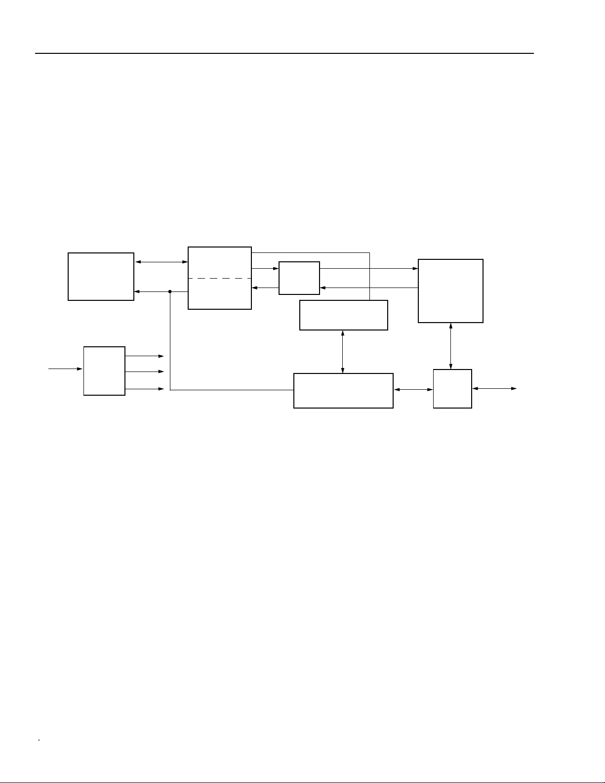
Figure 1 illustrates a functional overview of the LU6612
while Figure 2 details the functions. Figure 3 shows
how the LU6612 interfaces to the twisted pair.
IEEE
802.3u.
IEEE
802.3u.
IEEE
802.3u.
IEEE
802.3u 100Base-X specification.
LSCLK
25 MHz
MII/SERIAL
INTERFACE
DPLL
25 MHz
125 MHz
20 MHz
MANAGEMENT
PMA
PCS
AUTONEGOTIATION
10 Mbits/s TRANSCEIVER
DRIVER AND FILTERS
Figure 1. Functional Block Diagram: Device Overview
TX
PMD
DRIVER AND
FILTERS
MUX
TO/FROM
MAGNETICS
5-5600(F).r1
44 Lucent Technologies Inc.
Page 5
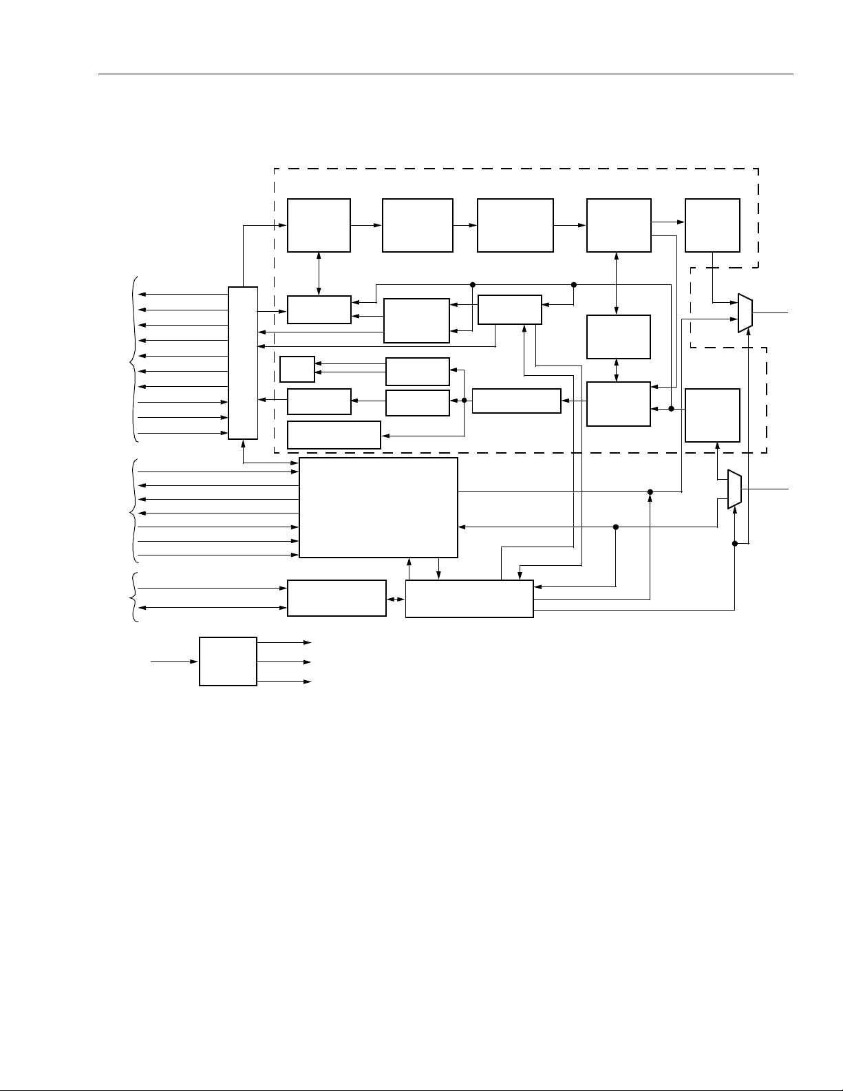
Data Sheet LU6612
Jul y 200 0
FASTCAT
Single-FET for 10Base-T/100Base-TX
Description
RXD[3:0]
RX_DV
RX_ER/RXD[4]
MII
INTERFACE
SERIAL
INTERFACE
RX_CLK
TX_CLK
TXD[3:0]
TX_EN
TX_ER/TXD[4]
REF10
CLK20
(continued)
TXD[3:0]
CRS
COL
MII
RXC
RXD
TXC
TEN
TXD
100 Mbits/s TRANSCEIVER
4B/5B
ENCODER
TX STATE
MACHINE
CIM
5B/4B
DECODER
FAR-END
FAULT DETECT
10 Mbits/s TRANSCEIVER
SD
CAR_STAT
RXERR_ST
FAR-END
FAULT GEN
COLLISION
DETECT
CARRIER
DETECT
ALIGNER
LC10 LS10
SCRAMBLER
RX STATE
MACHINE
SD
DESCRAMBLER
LC100
LS100
SD
PDT
DCRU
PDR
SD
PMD
TX
PMD
RX
TX/TY
RX/RY
MDC
MDIO
INTERFACE
MANAGEMENT
LSCLK
DPLL
25 MHz
125 MHz
20 MH
MII
MANAGEMENT
Z
AUTONEGOTIATION
AND LINK MONITOR
5-5136(F).cr1
Figure 2. Functional Block Diagram: Device Detail
Lucent Technologies Inc. 5
Page 6
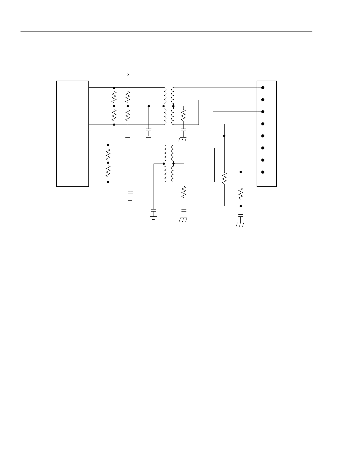
LU6612 Data Sheet
FASTCAT
Single-FET for 10Base-T/100Base-TX July 2000
Description
(continued)
8
9
LU6612
63
64
TX
TY
RX
RY
50
50
Ω
Ω
50
50
0.01 µF
DD
V
1:1
Ω
220
Ω
220
0.01 µF
Ω
Ω
1:1
0.01 µF
Ω
75
0.001 µF
Ω
75
0.001 µF
75
Ω
Ω
75
0.01 µF
RJ-45
1
2
3
4
5
6
7
8
Figure 3. Typical Twisted-Pair (TP) Interface
5-5433.i.r3
6 Lucent Technologies Inc.
Page 7
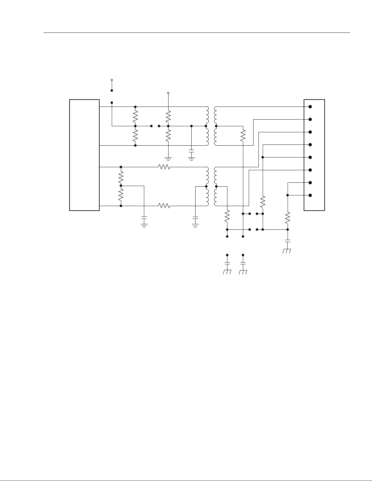
Data Sheet LU6612
Jul y 200 0
FASTCAT
Single-FET for 10Base-T/100Base-TX
Description
LU6612
QS6612
(continued)
VDD
TX
8
Q = 86.6
Q = 86.6
TY
9
RX
63
RY
64
Q = 0
Ω
L = OPEN
L = 50
L = 50
Q = 60
L = 50
L = 50
Q = 0
VDD
RJ-45
L = 1:1; Q = 1.25:1
Ω
Ω
Ω
Ω
Ω
Ω
Ω
Ω
L = 0
Q = OPEN
L = 0.01 µF
Q = OPEN
Ω
L = 0
L = 0
Q = 20
Q = 20
L = 0
Q = 20
L = 220
Q = 39
L = 220
Q = OPEN
Ω
Ω
Ω
Ω
Ω
Ω
L = 0.01 µF
Q = 0.1 µF
Ω
Ω
Ω
L = 0.01
Q = 0.1 µF
Ω
L = Q = 1:1
L = Q = 75
L = 0
Q = OPEN
L = Q = 75
Ω
Ω
Ω
Q = 0
Ω
L = OPEN
Q = 0
Ω
L = OPEN
L = 0
Ω
Q = OPEN
L = Q = 75
Ω
L = Q = 75
L = 0.01 µF
Q = 1000 pF
1
2
3
4
5
6
7
8
Ω
Key:
L = Lucent’s LU6612.
Q = Quality Semiconductor Inc. QS6612.
Figure 4. Onboard Universal Twisted-Pair Interface Circuit to Interchange Lucent and
Quality Semiconductor Inc. Parts
L = 0.001 µF L = 0.001 µF
5-5433.j
Lucent Technologies Inc. 7
Page 8

LU6612 Data Sheet
FASTCAT
Single-FET for 10Base-T/100Base-TX July 2000
Pin Information
VCCBG
ISET_100
GNDBG
LINKLED/PHYAD[0]
ACTLED/PHYAD[1]
CC
V
IOA
GNDIOA
TX
TY
GNDT
CC
V
CLKREF
GNDBT
CC
V
BT
TEST[0]
TEST[1]
REC
EQAP
CC
CC
V
V
RY
RX
GNDEQAP
60
61
62
63
64
1
2
3
4
5
6
7
8
9
10
11
T
12
13
14
15
16
17
18
19
20
21
GNDREC
59
22
BGREF[1]
BGREF[0]
57
58
LU6612
23
24
IOB
CC
MODE[2]
GNDIOB
V
FUDUPLED/PHYAD[3]
SPEEDLED/PHYAD[2]
52
53
54
55
56
25
26
27
28
29
DIGB
CC
MODE[0]
MODE[1]
V
49
50
51
30
48
GNDDIGB
47
TX_CLK
46
RX_ER/RXD[4]
45
RX_DV
44
RX_CLK
43
COL
42
CRS
41
GNDIOC
40
RXD[0]
39
RXD[1]
38
RXD[2]
37
RXD[3]
36
GNDDIGA
35
34
33
31
32
CC
V
DIGA
TXD[0]
TXD[1]
PLL
CC
PCSEN
V
TEST[2]
LSCLK1
LSCLK2
PHYAD[4]
GNDPLL
MDIO
ISET_10
MDC
RESET
RX_EN
TX_EN
TXD[3]
TXD[2]
TX_ER/TXD[4]
5-5866.r2
Figure 5. LU6612 Pinout
8 Lucent Technologies Inc.
Page 9

Data Sheet LU6612
Jul y 200 0
FASTCAT
Single-FET for 10Base-T/100Base-TX
Pin Information
(continued)
Pin Descriptions
Table 1. MII/Serial Interface Pins (17)
Signal Type Pin Description
COL O 43
CRS O 42
RX_CLK O 44
RXD[3:0] O 37:40
RX_DV O 45
RX_ER/
O46
RXD[4]
TX_CLK O 47
TXD[3:0] I 31:34
TX_EN I 30
Collision Detect.
This signal signifies in half-duplex mode that a collision has
occurred on the network. COL is asserted high whenever there is transmit and
receive activity on the UTP media. COL is the logical AND of TX_EN and receive
activity , and is an asynchronous output. When SERIAL_SEL (register 30, bit 1) is high
and in 10Base-T mode, this signal indicates the jabber timer has expired. This signal
is held low in full-duplex mode.
Carrier Sense.
When CRS_SEL (register 29, bit 10) is low, CRS is asserted high
when either the transmit or receive is nonidle. This signal remains asserted throughout a collision condition. When CRS_SEL (register 29, bit 10) is high, CRS is
asserted on receive activity only.
Receive Clock.
25 MHz clock output in 100 Mbits/s mode, 2.5 MHz output in
10 Mbits/s nibble mode, 10 MHz in 10 Mbits/s serial mode. RX_CLK has a worst-case
45/55 duty cycle. RX_CLK provides the timing reference for the transfer of RX_DV,
RXD, and RX_ER signals.
Receive Data.
4-bit parallel data outputs that are synchronous to the falling edge of
RX_CLK. When RX_ER is asserted high in 100 Mbits/s mode, an error code will be
presented on RXD[3:0] where appropriate. The codes are as follows:
■
Packet errors: ERROR_CODES = 2h;
■
Link errors: ERROR_CODES = 3h (Packet and link error codes will only be
repeated if registers [29.9] and [29.8] are enabled.);
■
Premature end errors: ERROR_CODES = 4h;
■
Code errors: ERROR_CODES = 5h.
When SERIAL_SEL (register 30, bit 1) is active-high and 10 Mbits/s mode is selected,
RXD[0] is used for data output and RXD[3:1] are 3-stated.
Receive Data Valid.
When this pin is high, it indicates the LU6612 is recovering and
decoding valid nibbles on RXD[3:0], and the data is synchronous with RX_CLK.
RX_DV is synchronous with RX_CLK. This pin is not used in serial 10 Mbits/s mode.
Receive E rr or.
When high, RX_ER indicates the LU6612 has detected a coding error
in the frame presently being transferred. RX_ER is synchronous with RX_CLK. When
the encode/decode bypass (EDB) is selected through the MII management interface,
this output serves as the RXD[4] output. This pin is only valid when LU6612 is in
100 Mbits/s mode.
Transmit Clock.
25 MHz clock output in 100 Mbits/s mode, 2.5 MHz output in
10 Mbits/s MII mode, 10 MHz output in 10 Mbits/s serial mode. TX_CLK provides timing reference for the transfer of the TX_EN, TXD, and TX_ER signals. These signals
are sampled on the rising edge of TX_CLK.
Transmit Data.
4-bit parallel input synchronous with TX_CLK. When SERIAL_SEL
(register 30, bit 1) is active-high and 10 Mbits/s mode is selected, only TXD[0] is valid.
Transmit Enable.
When driven high, this signal indicates there is valid data on
TXD[3:0]. TX_EN is synchronous with TX_CLK. When SERIAL_SEL
(register 30, bit 1) is active-high and 10 Mbits/s mode is selected, this pin indicates
there is valid data on TXD[0].
Lucent Technologies Inc. 9
Page 10

LU6612 Data Sheet
FASTCAT
Single-FET for 10Base-T/100Base-TX July 2000
Pin Information
Table 1. MII/Serial Interface Pins (17)
Signal Type Pin Description
TX_ER/
TXD[4]
RX_EN I 28
Table 2. MII Management Pins (2)
Signal Type Pin Description
MDC I 26
MDIO IO 25
(continued)
I29
Transmit Coding Error.
tionally corrupt the byte being transmitted across the MII (00100 will be transmitted).
When the encoder/decoder bypass bit is set, this input serves as the TXD[4] input.
When in 10 Mbits/s mode and SERIAL_SEL (register 30, bit 1) is active-high, this pin
is ignored.
Receive Enable.
RX_DV) are enabled. This pin has an internal 100
Management Data Clock.
the MDIO signal. This signal may be asynchronous to RX_CLK and TX_CLK. The
standard clock rate is 2.5 MHz, the maximum clock rate is 12.5 MHz. When running
MDC above 6.25 MHz, MDC must be synchronous with LSCLK and have a setup time
of 15 ns and a hold time of 5 ns with respect to LSCLK.
Management Data Input/Output.
mation between LU6612 and the station management. Control information is driven by
the station management synchronous with MDC. Status information is driven by the
LU6612 synchronous with MDC.
(continued)
When driven high, this signal causes the encoder to inten-
When this pin is high, the outputs (RXD[3:0], RX_ER, RX_CLK,
This is the timing reference for the transfer of data on
This I/O is used to transfer control and status infor-
Ω
pull-up resistor.
k
Table 3. 10/100 Mbits/s Twisted-Pair (TP) Interface Pins (4)
Signal Type Pin Description
RX I 63
RY I 62
TX O 8
TY O 9
Received Data.
Manchester data from magnetics.
Received Data.
Manchester data from magnetics.
Transmit Data.
Manchester data to magnetics.
Transmit Data.
Manchester data to magnetics.
Positive differential received 125 Mbaud MLT3 or 10 Mbaud
Negative differential received 125 Mbaud ML T3 or 10 Mbaud
Positive differential transmit 125 Mbaud MLT3 or 10 Mbaud
Negative differential transmit 125 Mbaud MLT3 or 10 Mbaud
10 Lucent Technologies Inc.
Page 11

Data Sheet LU6612
g
[0]
[0]
g
g
y
y
[1]
[1]
g
g
Jul y 200 0
FASTCAT
Single-FET for 10Base-T/100Base-TX
Pin Information
(continued)
Table 4. Ground and Power Pins (21)
Signal Type Pin Description
IOA PWR 6 Digital +5 V power supply for I/O
V
CC
GNDIOA PWR 7 Digital ground for I/O
V
IOB PWR 54 Digital +5 V power supply for I/O
CC
GNDIOB PWR 53 Digital ground for I/O
GNDIOC PWR 41 Digital ground for I/O
V
DIGA PWR 35 Digital +5 V power supply for logic
CC
GNDDIGA PWR 36 Digital ground for logic
V
DIGB PWR 49 Digital +5 V power supply for logic
CC
GNDDIGB PWR 48 Digital ground for logic
V
REC PWR 60 Digital +5 V power supply for clock recovery circuit
CC
GNDREC PWR 59 Digital ground for clock recovery circuit
V
PLL PWR 20 Analog +5 V power supply for 10 MHz and 100 MHz PLL clock synthesizer
CC
GNDPLL PWR 23 Analog ground for 10 MHz and 100 MHz PLL clock synthesizer
V
T PWR 11 Analog +5 V power supply for transmitter
CC
GNDT PWR 10 Analog ground for transmitter
V
EQAP PWR 61 Analog +5 V power supply for equalizer and adaptation circuit
CC
GNDEQAP PWR 64 Analog ground for adaptation circuit.
V
BG PWR 1 Analog +5 V power supply for band-gap circuit
CC
GNDBG PWR 3 Analog ground band-gap circuit
V
BT PWR 14 Analog +5 V power supply for 10Base-T transmitter
CC
GNDBT PWR 13 Analog ground for 10Base-T transmitter
Table 5. Miscellaneous Pins (20)
Signal Type*Pin Description
LSCLK1 I 21
Local Symbol Cl ock.
25 MHz clock, ±100 ppm, 40%—60% duty cycle. This input is
connected to one terminal of a 25 MHz crystal or an external 25 MHz clock source.
LSCLK2 O 22
Local Symbol Clock.
25 MHz crystal feedback. This output is connected to the
other terminal of a 25 MHz crystal or an external 25 MHz. If LSCLK1 is driven from
an external clock source, LSCLK2 is left unconnected.
LINKLED/
PHYAD[0]
ACTLED/
PHYAD[1]
↑
*
indicates there is an internal pull-up; ↓ indicates there is an internal pull-down.
I/O 4
I/O 5
Link LED.
This pin indicates
as input and to set the PHYAD
PHYAD
to a high or if pulled low through a resistor, will set PHYAD[0] to a zero.
When this pin is pulled hi
LED output will be active-hi
Activit
LED.
This pin indicates transmit/receive activit
ood link status. At powerup/reset, this pin is sampled
bit. If pulled high through a resistor, this pin will set
h the LED output will be active-low, when pulled low the
h.
is sampled as input to set the PHYAD
will set PHYAD
zero. When this pin is pulled hi
the LED output will be active-hi
to a high or if pulled low through a resistor, will set PHYAD[1] to a
h the LED output will be active-low, when pulled low
h.
. At powerup/reset, this pin
bit. If pulled high through a resistor, this pin
Lucent Technologies Inc. 11
Page 12

LU6612 Data Sheet
p
g
[2]
g
[2]
g
p
g
[3]
g
[3]
g
FASTCAT
Single-FET for 10Base-T/100Base-TX July 2000
Pin Information
Table 5. Miscellaneous Pins (20)
(continued)
(continued)
Signal Type*Pin Description
SPEED-
LED/
PHYAD[2]
I/O 56
eed LED.
S
■
LED is active when in 100 Mbits/s operation.
■
LED is not active when in 10 Mbits/s operation.
This pin indicates the operatin
At powerup/reset, this pin is sampled as input and to set the PHYAD
h through a resistor, this pin will set PHYAD[2] to a high or if pulled low through a
hi
resistor, will set PHYAD
to a zero. When this pin is pulled high, the LED output will
be active-low, when pulled low, the LED output will be active-hi
FUDUPLED/
PHYAD[3]
I/O 55
Full-Du
lex LED.
This pin indicates the operatin
when link is up:
■
LED is active when in full-duplex mode of operation.
■
LED is not active when in half-duplex mode of operation.
At powerup/reset, this pin is sampled as an input to set the PHYAD
h through a resistor, this pin will set PHYAD[3] to a high or if pulled low through a
hi
resistor, will set PHYAD
to a zero. When this pin is pulled high, the LED output will
be active-low, when pulled low, the LED output will be active-hi
PHYAD[4] I
↑
17
PHYAD[4].
At powerup/reset, this pin is sampled as an input to set the PHY AD[4] bit.
If pulled high through a resistor, this pin will set PHYAD[4] to a high or if pulled low
through a resistor, will set PHYAD[4] to a zero.
up resistor.
MODE[2:0] I
↑
52:50
Mode Selection.
These pins carry encoded signals that are latched into the LU6612
upon powerup/reset and define specific modes of operation: half/full duplex, autonegotiation enabled/disabled, and tr ansceiver isolation. Ref er to Table 20 for the v arious
modes and how various registers are aff ected. Pins [52:50] have internal 100 kΩ pullups. If left floating, LU6612 will default to all capable, autonegotiation enabled mode.
TEST[0] I
↑
Test Enable Pin for Factory Testing.
15
This pin has an internal 100 kΩ pull-down
resistor. The pin can be either left floating or tied down.
TEST[2:1] I
↓
CLKREF I 12
RESET
I27
Test Enable Pin f or Factory Testing.
19,
16
resistors. These pins can either be left floating or tied low.
Clock Reference.
Connect this pin to a 1 nF ± 10% capacitor to ground.
Full Chip Reset (Active-Low).
These two pins have internal 50 kΩ pull-down
Reset is an active-low signal. Reset must be
asserted low for at least five LSCLK cycles. The LU6612 will come out of reset after
400 µs. LSCLK1 must remain running during reset.
BGREF[1:0] I 57:58
Band-Gap Reference.
Connect these pins to a 24.9 kΩ ± 1% resistor to ground. The
parasitic load capacitance should be less than 15 pF.
ISET_100 I 2
Current Set 100 Mbits/s.
An external reference resistor (24.9 kΩ) is placed from this
pin to ground to set the 100 Mbits/s TP driver transmit output level.
ISET_10 I 24
Current Set 10 Mbits/s.
An external reference resistor (22.1 kΩ) is placed from this
pin to ground to set the 10 Mbits/s TP driver transmit output level.
PCSEN
↑
I
PCS Enable (Active-Low).
18
When this pin is active-low, the encoded 5-bit symbols
appear on RXD[4:0] and TXD[4:0]. When this pin high, 4-bit data appears on
RXD[3:0] and TXD[3:0]. When PCSEN
is low, LU6 612 bypasses the 4B5B encoder/
decoder, the align function, the scrambler/descramb ler, and does not detect and generate J/K and R/T code groups at the start or end of frame. This pin has an internal
100 kΩ pull-up.
speed of LU6612:
bit. If pulled
h.
mode of LU6612 and is only valid
bit. If pulled
h.
This pin has an internal 100
k
Ω
pull-
↑
*
indicates there is an internal pull-up; ↓ indicates there is an internal pull-down.
12 Lucent Technologies Inc.
Page 13

Data Sheet LU6612
Jul y 200 0
FASTCAT
Single-FET for 10Base-T/100Base-TX
MII Station Management
Basic Operations
The primary function of station management is to transfer control and status information about the LU6612 to a
management entity. This function is accomplished by the MDC clock input, which has a maximum frequency of
12.5 MHz, along with the MDIO pin. The management interface (MII) uses MDC and MDIO to physically transport
information between the PHY and the station management entity.
A specific set of registers and their contents (described in Table 8) defines the nature of the information transferred
across this interface. Frames transmitted on the MII management interface will have the frame structure shown in
Table 6. The order of bit transmission is from left to right. Note that reading and writing of the management register
must be completed without interruption.
MII Management Frames
The fields and format for management frames are described in the following tables.
Table 6. MII Management Frame Fields and Format
Read/Write
(R/W)
R 1 . . . 1 01 10 AAAAA RRRRR Z0 DDDDDDDDDDDDDDDD Z
W 1 . . . 1 01 01 AAAAA RRRRR 10 DDDDDDDDDDDDDDDD Z
Table 7. MII Management Frame Descriptions
Field Description
Pre
ST
OP
PHYADD
REGAD
TA
DA TA
Pre ST OP PHYADD REGAD TA DATA Idle
Preamble.
This is indicated by a 1 in register 1, bit 6.
Start of Frame.
Operation Code.
transaction is 01.
PHY Address.
bit transmitted and received is the MSB of the address. A station management entity, which is
attached to multiple PHY entities, must have prior knowledge of the appropriate PHY address for
each entity. The address 00000 is the broadcast address. This address will produce a match
regardless of the local address.
Register Address.
The first register address bit transmitted and received is the MSB of the address.
Turnaround.
data field of a frame to avoid drive contention on MDIO during a read transaction. During a write to
the LU6612, these bits are driven to a 10 by the station. During a read, the MDIO is not driven during the first bit time and is driven to a 0 by the LU6612 during the second bit time.
Data.
addressed.
The preamble is a series of 32 1s. The LU6612 will accept frames with no preamble.
The start of frame is indicated by a 01 pattern.
The operation code for a read transaction is 10. The operation code for a write
The PHY address is 5 bits, allowing for 32 unique addresses. The first PHY address
The register address is 5 bits, allowing for 32 unique registers within each PHY.
The turnaround time is a 2-bit time spacing between the register address field and the
The data field is 16 bits. The first bit transmitted and received is bit 15 of the register being
Lucent Technologies Inc. 13
Page 14

LU6612 Data Sheet
FASTCAT
Single-FET for 10Base-T/100Base-TX July 2000
MII Station Management
Register Overview
The MII management 16-bit register (MR) set is implemented as described in Table 8 below.
Table 8. MII Management Registers (MR)
Register
Address
0 MR0 Control Register 3000
1 MR1 Status Register 7849
2 MR2 PHY Identifier Register 1 0180
3 MR3 PHY Identifier Register 2 7641
4 MR4 Autonegotiation Advertisement Register 01E1
5 MR5 Autonegotiation Link Partner Ability Register (Base_Page) 0000
5 MR5 Autonegotiation Link Partner Ability Register (Next_Page) —
6 MR6 Autonegotiation Expan si on Regi ster 0000
7 MR7 Next-Page Transmit Register 0000
8—27 MR8—MR27 Reserved 0000
28 MR28 Device Specific Register 1 0000
29 MR29 Device Specific Register 2 1000
30 MR30 Device Specific Register 3 0000
Symbol Name
(continued)
Default
(Hex Code)
14 Lucent Technologies Inc.
Page 15

Data Sheet LU6612
Jul y 200 0
FASTCAT
Single-FET for 10Base-T/100Base-TX
MII Station Management
(continued)
This section provides a detailed discussion of each management register and its bit definitions.
Table 9. MR0—Control Register Bit Descriptions
1
Bit
0.15 (SW_RESET) R/W
Type
2
Reset.
Description
Setting this bit to a 1 will reset the LU6612. All registers will be set to
their default state. This bit is self-clearing. The default is 0.
0.14 (LOOPBACK) R/W
Loopback.
When this bit is set to 1, no data transmission will take place on the
media. Any receive data will be ignored. The loopback signal path will contain
all circuitry up to, but not including, the PMD. The autonegotiation must be
turned off, before loopback can be initiated, transmit data can be started 2 ms
after loopback is initiated. The default value is a 0.
0.13 (SPEED100) R/W
Speed Selection.
The value of this bit reflects the current speed of operation
(1 = 100 Mbits/s; 0 = 10 Mbits/s). This bit will only affect operating speed when
the autonegotiation enable bit (register 0, bit 12) is disabled (0). This bit is
ignored when autonegotiation is enabled (register 0, bit 12). The bit is set high
when MODE[2:0] is 010 or 011 or 100. The default is 1.
0.12 (NWAY_ENA) R/W
Autonegotiation Enable.
The autonegotiation process will be enabled by setting this bit to a 1. This bit overrides SPEED100 bit (register 0, bit 13) and
FULL_DUP bit (register 0, bit 8). This bit is set high when MODE[2:0] is 100 or
111. Autonegotiation must be disabled before loopback can be initiated. The
default state is a 1.
0.11 (PWRDN) R/W
Powerdown.
The LU6612 may be placed in a low-power state by setting this
bit to a 1, both the 10 Mbits/s transceiver and the 100 Mbits/s transceiver will
be powered down. While in the powerdown state, the LU6612 will respond to
management transactions. The default state is a 0.
0.10 (ISOLATE) R/W
Isolate.
When this bit is set to a 1, the MII outputs will be brought to the high-
impedance state. The default state is a 0.
0.9 (REDONWAY) R/W
Restart Autonegotiation.
Normally, the autonegotiation process is started at
powerup. The process may be restarted by setting this bit to a 1. The default
state is a 0. The NWAYDONE bit (register 1, bit 5) is reset when this bit goes to
a 1. This bit is self-cleared when autonegotiation restarts.
0.8 (FULL_DUP) R/W
Duplex Mode.
This bit reflects the mode of operation (1 = full duplex; 0 = half
duplex). This bit is ignored when the autonegotiation enable bit (register 0,
bit 12) is enabled. The default state is a 0. This bit is set as a 1 during powerup/
reset, when MODE[2:0] is 001 or 011.
0.7 (COLTST) R/W
Collision Test.
When this bit is set to a 1, the LU6612 will assert the COL sig-
nal in response to TX_EN. This bit should only be set when in loopback mode.
0.6:0 NA
Reserved.
All bits will read 0.
1. Note that the format for the pin descriptions is as follo ws: the first number is the register number, the second number is the bit position in the
register, and the name of the instantiated pad is in capital letters.
2. R = read, W = write, NA = not applicable.
Lucent Technologies Inc. 15
Page 16

LU6612 Data Sheet
FASTCAT
Single-FET for 10Base-T/100Base-TX July 2000
MII Station Management
(continued)
Table 10. MR1—Status Register Bit Descriptions
1
Bit
1.15 (T4ABLE) R
Type
2
100Base-T4 Ability.
0: Not able
1: Able
1.14 (TXFULDUP) R
100Base-TX Full-Duplex Ability.
0: Not able
1: Able
1.13 (TXHAFDUP) R
100Base-TX Half-Duplex Ability.
0: Not able
1: Able
1.12 (ENFULDUP) R
10Base-T Full-Duplex Ability.
0: Not able
1: Able
1.11 (ENHAFDUP) R
10Base-T Half-Duplex Ability.
0: Not able
1: Able
1.10:7 R
1.6 (NO_PA_OK) R
Reserved.
All bits will read as a 0.
Suppress Preamble.
management frames with the preamble suppressed. (This function is not suppor ted by QS6611.)
1.5 (NWAYDONE) R
Autonegotiation Complete.
process has been completed. The contents of registers MR4, MR5, MR6, and
MR7 are now valid. The default value is a 0. This bit is reset when autonegotiation is started.
1.4 (REM_FLT) R
Remote Fault.
When this bit is a 1, it indicates a remote fault has been detected.
This bit will remain set until cleared by reading the register. The default is a 0.
1.3 (NWAYABLE) R
Autonegotiation Ability.
autonegotiation. The value of this bit is always a 1.
1.2 (LSTAT_OK) R
Link Status.
When this bit is a 1, it indicates a valid link has been established.
This bit has a latching function: a link failure will cause the bit to clear and stay
cleared until it has been read via the management interface.
1.1 (JABBER) R
Jabber Dete ct.
This bit will be a 1 whenever a jabber condition is detected. It will
remain set until it is read, and the jabber condition no longer exists.
1.0 (EXT_ABLE) R
Extended Capability.
register set (MR2 and beyond). It will always read a 1.
Description
This bit will always be a 0.
This bit will always be a 1.
This bit will always be a 1.
This bit will always be a 1.
This bit will always be a 1.
This bit is set to a 1, indicating that the LU6612 accepts
When this bit is a 1, it indicates the autonegotiation
When this bit is a 1, it indicates the ability to perform
This bit indicates that the LU6612 supports the extended
1. Note that the format for the pin descriptions is as follows: the first number is the register number, the second number is the bit position in the
register, and the name of the instantiated pad is in capital letters.
2. R = read.
16 Lucent Technologies Inc.
Page 17

Data Sheet LU6612
Jul y 200 0
FASTCAT
Single-FET for 10Base-T/100Base-TX
MII Station Management
(continued)
Table 11. MR2, 3—PHY Identifier Registers (1 and 2) Bit Descriptions
1
Bit
2.15:0 (OUI[3:18]) R
Type
2
Organizationally Unique Identifier.
Description
The third through the 24th bits of the
OUI assigned to the PHY manufacturer by the
IEEE
are to be placed in bits
2.15:0 and 3.15:10. The value for bits 15:0 of register 2 is 0180h.
3.15:10 (OUI[19:24]) R
Organizationally Unique Identifier.
The remaining 6 bits of the OUI. The
value for bits 15:10 of register 3 is 1Dh.
3.9:4 (MODEL[5:0]) R
Model Numb er.
6-bit model number of the device. The model number is 12
decimal.
3.3:0 (VERSION[3:0]) R
Revision Number .
The value of the present revision number. The value is
0001b for the first version.
1. Note that the format for the pin descriptions is as follo ws: the first number is the register number, the second number is the bit position in the
register, and the name of the instantiated pad is in capital letters.
2. R = read.
Table 12. MR4—Autonegotiation Advertisement Register Bit Descriptions
1
Bit
4.15 (NEXT_PAGE) R/W
Type
2
Next Page.
Description
The next page function is activated by setting this bit to a 1.
This will allow the exchange of arbitrary pieces of data. Data is carried by
optional next pages of information. (This function is not supported by
QS6611.)
4.14 (ACK) R/W
4.13 (REM_FAULT) R/W
Acknowledge.
Remote Fault.
This bit is written to a logic zero and ignored on read.
When set to 1, the LU6612 indicates to the link partner a
remote fault condition.
4.12:10 (PAUSE) R/W
Pause.
When set to 1, indicates that the LU6612 wishes to exchange flow
control information with its link partner.
4.9 (100BASET4) R/W
4.8 (100BASET_FD) R/W
100Base-T4.
This bit should always be set to a 0.
100Base-TX Full Duplex.
If written to 1, autonegotiation will advertise that
the LU6612 is capable of 100Base-TX full-duplex operation. This bit is set
high when MODE[2:0] is 111.
4.7 (100BASETX) R/W
100Base-TX.
If written to 1, autonegotiation will advertise that the LU6612
is capable of 100Base-TX operation.
4.6 (10BASET_FD) R/W
10Base-T Full Duplex.
If written to 1, autonegotiation will advertise that the
LU6612 is capable of 10Base-T full-duplex operation. This bit is set high
when MODE[2:0] is 111.
4.5 (10BASET) R/W
10Base-T.
If written to 1, autonegotiation will advertise that the LU6612 is
capable of 10Base-T operation. This bit is set high when MODE[2:0] is 111.
4.4:0 (SELECT) R/W
Selector Field.
Reset with the value 00001 for
IEEE
802.3.
1. Note that the format for the pin descriptions is as follo ws: the first number is the register number, the second number is the bit position in the
register, and the name of the instantiated pad is in capital letters.
2. R = read, W = write.
Lucent Technologies Inc. 17
Page 18

LU6612 Data Sheet
FASTCAT
Single-FET for 10Base-T/100Base-TX July 2000
MII Station Management
(continued)
Table 13. MR5—Autonegotiation Link Partner (LP) Ability Register Bit Descriptions (Base_Page)
1
Bit
5.15 (LP_NEXT_PAGE) R
Type
2
Link Partner Next Page.
Description
When this bit is set to 1, it indicates that the link
partner wishes to engage in next page exchange.
5.14 (LP_ACK) R
Link Partner Acknowledge.
When this bit is set to 1, it indicates that the link
partner has successfully received at least three consecutive and consistent
FLP bursts.
5.13 (LP_REM_FAULT) R
Link Partner Remote Fault.
When this bit is set to 1, it indicates that the link
partner has a fault.
5.12:10 R
5.9 (LP_100BASET4) R
Reserved.
These bits are reserved.
Link Partner 100Base-T4.
When this bit is set to 1, it indicates that link part-
ner is capable of 100Base-T4 operation.
5.8 (LP_100BASET_FD) R
Link Partner 100Base-TX Full Duplex.
When this bit is set to 1, it indicates
that link partner is capable of 100Base-TX full-duplex operation.
5.7 (LP_100BASETX) R
Link Partner 100Base-TX.
When this bit is set to 1, it indicates that link part-
ner is capable of 100Base-TX operation.
5.6 (LP_10BASET_FD) R
Link Partner 10Base-T Full Duplex.
When this bit is set to 1, it indicates that
link partner is capable of 10Base-T full-duplex operation.
5.5 (LP_10BASET) R
Link Partner 10Base-T.
When this bit is set to 1, it indicates that link partner
is capable of 10Base-T operation.
5.4:0 (LP_SELECT) R
Selector Field.
ner. For
IEEE
802.3 compliant link partners, this field should read 00001.
This field contains the type of message sent by the link part-
1. Note that the format for the pin descriptions is as follows: the first number is the register number, the second number is the bit position in the
register, and the name of the instantiated pad is in capital letters.
2. R = read.
Table 14. MR5—Autonegotiation Link Partner (LP) Ability Register Bit Descriptions (Next_Page)
1
Bit
5.15 (LP_N E XT_PAGE) R
Type
2
Next Page.
Description
When this bit is set to a logic 0, it indicates that this is the last
page to be transmitted. A logic 1 indicates that additional pages will follow.
5.14 (LP_ACK) R
Acknowledge.
When this bit is set to a logic 1, it indicates that the link part-
ner has successfully received its partner’s link code word.
5.13 (LP_MES_PAGE) R
Message Page.
This bit is used by the Next_Page function to differentiate a
Message Page (logic one) from an unformatted page (logic zero).
5.12 (LP_ACK2) R
Acknowledge 2.
This bit is used by Next_Page function to indicate that a
device has the ability to comply with the message (logic one) or not (logic
zero).
5.11 (LP_TOGGLE) R
Toggle.
This bit is used by the arbitration function to ensure synchronization
with the link partner during next page exchange. Logic 0 indicates that the
previous value of the transmitted link code word was logic 1. Logic 1 indicates
that the previous value of the transmitted link code word was logic 0.
5.10:0 (MCF) R
Message/Unformatted Code Field.
With these 11 bits, there are 2048 possible messages. Message code field definitions are described in annex 28C of
the
IEEE
802.3u standard.
1. Note that the format for the pin descriptions is as follows: the first number is the register number, the second number is the bit position in the
register, and the name of the instantiated pad is in capital letters.
2. R = read.
18 Lucent Technologies Inc.
Page 19

Data Sheet LU6612
Jul y 200 0
FASTCAT
Single-FET for 10Base-T/100Base-TX
MII Station Management
(continued)
Table 15. MR6—Autonegotiation Expansion Register Bit Descriptions
1
Bit
6.15:5 R
6.4 (PAR_DET_FAULT) R/LH
Type
2
Reserved.
Parallel Detection Fault.
Description
When this bit is set to 1, it indicates that a fault
has been detected in the parallel detection function. This fault is due to more
than one technology detecting concurrent link conditions. This bit can only
be cleared by reading this register.
6.3
(LP_NEXT_PAGE_ABLE)
6.2 (NEXT_PAGE_ABLE) R
Link Partner Next Page Able.
R
When this bit is set to 1, it indicates that the
link partner supports the next page function.
Next Page Able.
This bit is set to 1, indicating that this device supports the
next page function.
6.1 (PAGE_REC) R/LH
Page Received.
When this bit is set to 1, it indicates that a next page has
been received.
6.0 (LP_NWAY_ABLE) R
Link Partner Autonegotiation Capable.
When this bit is set to 1, it indi-
cates that the link partner is autonegotiation capable.
1. Note that the format for the pin descriptions is as follo ws: the first number is the register number, the second number is the bit position in the
register, and the name of the instantiated pad is in capital letters.
2. R = read, LH = latched high.
Table 16. MR7—Next_Page Transmit Register Bit Descriptions
1
Bit
7.15 (NEXT_PAGE) R/W
Type
2
Next Page.
Description
This bit indicates whether or not this is the last next page to be transmitted. When this bit is 0, it indicates that this is the last page. When this bit is 1, it
indicates there is an additional next page.
7.14 (ACK) R
7.13 (MESSAGE) R/W
Acknowledge.
Message Page.
This bit is the acknowledge bit from the link code word.
This bit is used to differentiate a message page from an unformatted page. When this bit is 0, it indicates an unformatted page. When this bit is
1, it indicates a formatted page.
7.12 (ACK2) R/W
Acknowledge 2.
This bit is used by the next page function to indicate that a
device has the ability to comply with the message. Acknowledge 2 will be set as
follows:
■
When this bit is 0, it indicates the device cannot comply with the message.
■
When this bit is 1, it indicates the device will comply with the message.
7.11 (TOGGLE) R
Toggle.
This bit is used by the arbitration function to ensure synchronization with
the link partner during next page exchange. This bit will always take the opposite
value of the toggle bit in the previously exchanged link code word:
■
If the bit is a logic 0, the previous value of the transmitted link code word was a
logic 1.
■
If the bit is a 1, the previous value of the transmitted link code word was a 0.
The initial value of the toggle bit in the first next page transmitted is the inverse of
the value of bit 11 in the base link code word and, therefore, may assume a value
of 1 or 0.
7.10:0 (MCF) R/W
Message/Unformatted Code Field.
With these 11 bits, there are 2048 possible
messages. Message code field definitions are described in annex 28C of the
IEEE
802.3u standard.
1. Note that the format for the pin descriptions is as follo ws: the first number is the register number, the second number is the bit position in the
register, and the name of the instantiated pad is in capital letters.
2. R = read, W = write.
Lucent Technologies Inc. 19
Page 20

LU6612 Data Sheet
FASTCAT
Single-FET for 10Base-T/100Base-TX July 2000
MII Station Management
(continued)
Table 17. MR28—Device-Specific Register 1 (Status Register) Bit Descriptions
1
Bit
28.15:9 (R28[15:9]) R
28.8 (BAD_FRM) R/LH
Type
2
Unused.
Bad Frame.
Description
Read as 0.
If this bit is a 1, it indicates a packet has been received without an
SFD. This bit is only valid in 10 Mbits/s mode.
This bit is latching high and will only clear after it has been read or the device has
been reset. The default is 0.
28.7 (CODE) R/LH
Code Violation.
When this bit is a 1, it indicates a Manchester code violation has
occurred. The error code will be output on the RXD lines. Refer to Table 1 for a
detailed description of the RXD pin error codes. This bit is only valid in 10 Mbits/s
mode.
This bit is latching high and will only clear after it has been read or the device has
been reset. The default is 0.
28.6 (APS) R
Autopolarity Status.
When register 30, bit 3 is set and this bit is a 1, it indicates
the LU6612 has detected and corrected a polarity reversal on the twisted pair.
If the APF_EN bit (register 30, bit 3) is set, the reversal will be corrected inside the
LU6612. This bit is not valid in 100 Mbits/s operation. The default is 0.
28.5 (DISCON) R/LH
Disconnect.
If this bit is a 1, it indicates a disconnect. This bit will latch high until
read. This bit is only valid in 100 Mbits/s mode. The default is 0.
28.4 (UNLOCKED) R/LH
Unlocked.
Indicates that the TX scrambler lost lock. This bit will latch high until
read. This bit is only valid in 100 Mbits/s mode. The default is 0.
28.3 (RXERR_ST) R/LH
RX Error Status.
Indicates a false carrier. This bit will latch high until read. This
bit is only valid in 100 Mbits/s mode. The default is 0.
28.2 (FRC_JAM) R/LH
Force Jam.
This bit will latch high until read. This bit is only valid in 100 Mbits/s
mode. The default is 0.
28.1 (LNK100UP) R
Link Up 100.
This bit, when set to a 1, indicates a 100 Mbits/s transceiver is up
and operational. The default is 0.
28.0 (LNK10UP) R
Link Up 10.
This bit, when set to a 1, indicates a 10 Mbits/s transceiver is up and
operational. The default is 0.
1. Note that the format for the pin descriptions is as follows: the first number is the register number, the second number is the bit position in the
register, and the name of the instantiated pad is in capital letters.
2. R = read, LH = latched high.
20 Lucent Technologies Inc.
Page 21

Data Sheet LU6612
Jul y 200 0
FASTCAT
Single-FET for 10Base-T/100Base-TX
MII Station Management
Table 18. MR29—Device-Specific Register 2 (100 Mbits/s Control) Bit Descriptions
1
Bit
29.15 (LOCALRST) R/W
29.14 (RST1) R/W
29.13 (RST2) R/W
29.12 (100OFF) R/W
29.11 R/W
29.10 (CRS_SEL) R/W
29.9 (LINK_ERR) R/W
29.8 (PKT_ERR) R/W
29.7 (RESERVED) R/W
29.6 (EDB) R/W
29.5 (SAB) R/W
29.4 (SDB) R/W
29.3 (CARIN_EN) R/W
29.2 (JAM_COL) R/W
29.1 (RESERVED) R/W
29.0 (RESERVED) R/W
Type
(continued)
2
Management Reset.
this bit will cause the lower 16 registers and registers 28 and 29 to be reset to
their default values. This bit is self-clearing. The default is 0.
Generic Reset 1.
Generic Reset 2.
100 Mbits/s Transmitter Off.
high. This bit defaults to 1.
Reserved.
Carrier Sense Select.
a 1. If this bit is set to logic 0, CRS will be asserted on receive or transmit. The
default is 0.
Link Error Indication.
RXD[3:0] of the LU6612 when RX_ER is asserted on the MII. The specific error
codes are listed in the RXD pin description. If it is 0, it will disable this function.
The default is 0.
Packet Error Indication Enable.
indicates that the scrambler is not locked, will be reported on RXD[3:0] of the
LU6612 when RX_ER is asserted on the MII. When this bit is 0, it will disable this
function. The default is 0.
Reserved.
Encoder/Decoder Bypass.
5B/4B decoder function will be disabled. The default is a zero. At powerup/reset, if
PCSEN
Symbol Aligner Bypass.
abled. The default is 0.
Scrambler/Descrambler Bypass.
descramb li ng f un ctio ns w ill be d isa b led . Th e de f au lt is a z ero. At powerup/ rese t, if
PCSEN
Carrier Integrity Enable.
(This function is not supported by QS6611.) The default is 0.
Jam Enable.
to be ORed with COL. The default is 0.
Reserved.
Reserved.
Program to zero.
This bit must remain as a zero. The default is 0.
is strapped low, then this bit is set to a 1. The default is 0.
is strapped low, then this bit is set to a 1. The default is 0.
When this bit is a 1, it enables JAM associated with carrier integrity
This bit must remain as a zero. The default is 0.
This bit must remain as a zero. The default is 0.
This is the local management reset bit. Writing a logic 1 to
This register is used for manufacture test only. The default is 0.
This register is used for manufacture test only. The default is 0.
CRS will be asserted on receive only when this bit is set to
When this bit is a 1, a link error code will be reported on
When this bit is set to 1, the aligner function will be dis-
When this bit is set to a 1, carrier integrity is enabled.
Description
When this bit is set to 0, it forces RX low and RY
When this bit is a 1, a packet error code, which
When this bit is set to 1, the 4B/5B encoder and
When this bit is set to 1, the scrambling/
1. Note that the format for the pin descriptions is as follo ws: the first number is the register number, the second number is the bit position in the
register, and the name of the instantiated pad is in capital letters.
2. R = read, W = write.
Lucent Technologies Inc. 21
Page 22

LU6612 Data Sheet
FASTCAT
Single-FET for 10Base-T/100Base-TX July 2000
MII Station Management
(continued)
Table 19. MR30—Device-Specific Register 3 (10 Mbits/s Control) Bit Descriptions
1
Bit
30.15:6 (R30[15:6]) R/W
30.5 (HBT_EN) R/W
Type
2
Unused.
Heartbeat Enable .
Description
Read as 0.
When this bit is a 1, the heartbeat function will be
enabled. Valid in 10 Mbits/s mode only. The default is 0.
30.4 (ELL_EN) R/W
Extended Line Length Enable.
When this bit is a 1, the receive squelch levels are reduced from a nominal 435 mV to 350 mV, allowing reception of signals with a lower amplitude. Valid in 10 Mbits/s mode only. The default is 0.
30.3 (APF_EN) R/W
Autopolarity Function Enable.
When this bit is a 1 and the LU6612 is in
10 Mbits/s mode, the autopolarity function will determine if the TP link is wired
with a polarity reversal. If there is a polarity reversal, the LU6612 will assert
the APS bit (register 28, bit 6) and correct the polarity reversal. If this bit is a 0
and the device is in 10 Mbits/s mode, the reversal will not be corrected. The
default is 0.
30.2 (REF_SEL) R/W
Reference Select.
When this bit is a 1, the external 10 MHz reference of pin
REF10 is used for phase alignment. This bit defaults to a 0.
30.1 (SERIAL _SEL) R/W
Serial Select.
When this bit is set to a 1, 10 Mbits/s serial mode will be
selected. When the LU6612 is in 100 Mbits/s mode, this bit will be ignored.
The default is 0.
30.0 (ENA_NO_LP) R/W
No Link Partner Mode.
Setting this bit to a 1 will allow 10 Mbits/s operation
with link pulses disabled. If the LU6612 is configured for 100 Mbits/s operation, setting this bit will not affect operation. The default is 0.
1. Note that the format for the pin descriptions is as follows: the first number is the register number, the second number is the bit position in the
register, and the name of the instantiated pad is in capital letters.
2. R = read, W = write.
22 Lucent Technologies Inc.
Page 23

Data Sheet LU6612
Jul y 200 0
FASTCAT
Single-FET for 10Base-T/100Base-TX
MODE Selection
LU6612 can be forced to operate in specific operating modes. This is achieved by configuring the MODE pins to
the appropriate values at powerup/reset. The strapping options of the MODE pins are latched on reset to set the
default values of various registers. The values can be modified by writing into the registers. The MODE[2:0] pins
have 100 kΩ internal pull-ups. If MODE[2:0] are left floating, LU6612 will default to all capable, autonegotiation
enabled mode.
The different modes of operation of LU6612 and the register bits affected are presented in the following table.
Table 20. Operation Modes of LU6612
MODE
[2:0]
000 10Base-T, half-duplex with autonegotiation disabled 0 0 0 0101
00110Base-T, full-duplex with autonegotiation disabled 1000111
010100Base-TX, half-duplex with autonegotiation disabled 0001001
011 100Base-TX, full-duplex with autonegotiation disabled 1 0 0 1001
100Advertise 100Base-TX, half-duplex autonegotiation enabled 0011000
101Reserved ———————
110Isolate MII 0101110
111 All capable, autonegotiation enabled 0 0 1 1111
Table 21. LU6612 Crystal Specifications
Parameter Requirement
Type Quartz Fundamental Mode
Frequency 25 MHz
Stability ±25 ppm, 0—70 °C
Shunt Capacitor 7 pF
Load Capacitor 20 pF
Series Res istance <30 Ω
Definition
0.8 0.10 0.12 0.13 4.5 4.6 4.8
Register.Bit
Lucent Technologies Inc. 23
Page 24

LU6612 Data Sheet
FASTCAT
Single-FET for 10Base-T/100Base-TX July 2000
Absolute Maximum Ratings
(TA = 25 °C)
Stresses in excess of the absolute maximum ratings can cause permanent damage to the device. These are absolute stress ratings only. Functional operation of the device is not implied at these or any other conditions in excess
of those given in the operational sections of the data sheet. Exposure to absolute maximum ratings for extended
periods can adversely affect device reliability.
Table 22. Absolute Maximum Ratings
Parameter Symbol Min Max Unit
stg
A
070°C
–40 125 °C
DD
+ 0.5 V
Ambient Operating Temperature T
Storage Temperature T
Voltage on Any Pin with Respect to Ground — –0.5 V
Maximum Supply Voltage — — 5.5 V
Table 23. Operating Conditions
Parameter Symbol Min Typ
*
Max Unit
Operating Supply Voltage — 4.75 5.0 5.25 V
Power Dissipation:
100 Mbits/s TX
10 Mbits/s
Autonegotiating
D
P
D
P
D
P
—
—
—
1.4
1.0
1.0
1.6
1.35
—
W
W
mW
* Typical power dissipations are specified at 5.0 V and 25 °C. This is the power dissipated by the LU6612 transmitting over 100 meters of cable.
Electrical Characteristics
The following specifications apply for VDD = 5 V ± 5%.
Table 24. dc Characteristics
Parameter Symbol Min Typ Max Unit
TTL Inputs:
Input High Voltage
Input Low Voltage
Input High Current
Input Low Current
Input Leakage Current
TTL Outputs:
Output High Voltage
Output Low Voltage
Output Short-circuit Current
10 Mbits/s Twisted Pair: Input V oltage V
100 Mbits/s Twisted Pair: Input Voltage V
10 Mbits/s Twisted Pair: Output Current V
100 Mbits/s Twisted Pair: Output Current V
V
V
I
V
V
I
IH
IL
IH
IL
I
L
I
OH
OL
SC
DIFF
DIFF
DIFF
DIFF
2.0
—
—
—
—
2.4
—
–15
—
—
—
—
—
—
—
—
—
0.8
50
–400
50
—
0.45
–85
0.35 — 2.0 V
——1.5V
45 50 55 mA
19 20 21 mA
V
V
µA
µA
µA
V
V
mA
24 Lucent Technologies Inc.
Page 25

Data Sheet LU6612
Jul y 200 0
FASTCAT
Single-FET for 10Base-T/100Base-TX
Timing Characteristics (Preliminary)
Table 25. MII Management Interface Timing (25 pF Load)
Name Parameter Min Typ Max Unit
t1 MDIO Valid to Rising Edge of MDC (setup) 10 — — ns
t2 Rising Edge of MDC to MDIO Invalid (hold) 10 — — ns
t3 MDC Falling Edge to MDIO Valid (prop. delay) 0 — 40 ns
t4 MDC High* — 200 — ns
t5 MDC Low* 40 200 — ns
t6 MDC Period* 80 400 — ns
* When operating MDC above 6.25 MHz, MDC must be synchronous with LSCLK and have a setup time of 15 ns and a hold time of 5 ns,
with respect to LSCLK.
MDC
MDIO
MDC
t1
t2
Figure 6. MDIO Input Timing
t6
MDC
t5 t4
MDIO
t3
Figure 7. MDIO Output Timing
< R > < Z > < O >
5-4959(F).a
5-4960(F).c
MDIO
5-5312(F).r1
Note: MDIO turnaround (TA) time is a 2-bit time spacing between the register address field, and the data field of a frame to avoid drive conten-
tion on MDIO during a read transaction. During a write to the LU6612, these bits are driven to a 10 by the station. During a read, the
MDIO is not driven during the first bit time and is driven to a 0 by the LU6612 during the second bit time.
Figure 8. MDIO During TA (Turnaround) of a Read Transaction
Lucent Technologies Inc. 25
Page 26

LU6612 Data Sheet
FASTCAT
Single-FET for 10Base-T/100Base-TX July 2000
Timing Characteristics (Preliminary)
Table 26. MII Data Timing (25 pF Load)
Name Parameter Min Typ Max Unit
t1 RXD[3:0], RX_ER, RX_DV, Valid to RX_CLK High 10/100 — — ns
t2 RX_CLK High to RXD[3:0], RX_DV, RX_ER Invalid 10/100 — — ns
t3 RX_CLK High 14/180 — 26/220 ns
t4 RX_CLK Low 14/180 — 26/220 ns
t5 RX_CLK Period — 40 — ns
t6 TX_CLK High 14/180 — 26/220 ns
t7 TX_CLK Low 14/180 — 26/220 ns
t8 TX_CLK Peri od — 40 — ns
t9 TXD[3:0], TX_EN, TX_ER, Setup to TX_CLK 15/140 — — ns
t10 TXD[3:0], TX_EN, TX_ER, Hold to TX_CLK 0/0 — — ns
t11 TXD[3:0], TX_EN, TX_ER Setup to LSCLK* 10 — — ns
t12 TXD[3:0], TX_EN, TX_ER, Hold to LSCLK* 0 — — ns
t13 First Bit of J on RX/RY While Transmitting Data to COL
Assert (half-duplex mode)
t14 First Bit of T Received on RX/RY While Transmitting to COL
Deasser ted (h alf -dupl ex mode)
* 100 Mbits/s only.
(continued)
——170ns
——210ns
26 Lucent Technologies Inc.
Page 27

Data Sheet LU6612
Jul y 200 0
FASTCAT
Single-FET for 10Base-T/100Base-TX
Timing Characteristics (Preliminary)
RX_CLK
RXD[3:0]
RX_DV
RX_ER
t1
TX_CLK
TXD[3:0]
TX_EN
TX_ER
(continued)
t5
t3t4
t7
t2
t8
t6
t9
t10
LSCLK
TXD[3:0]
TX_EN
TX_ER
RX/RY
COL
t13
t11
1st BIT OF J
t12
1st BIT OF T
t14
Figure 9. MII Timing Requirements for LU6612
5-5432(F).cr1
Lucent Technologies Inc. 27
Page 28

LU6612 Data Sheet
FASTCAT
Single-FET for 10Base-T/100Base-TX July 2000
Timing Characteristics (Preliminary)
(continued)
Table 27. Serial 10 Mbits/s Timing for RX/RY, CRS, and RX_CLK
Name Parameter Min Max Unit
t15 RX/RY Activity to CRS Assertion 40 500 ns
t16 RX/RY Activity to RX_CLK Valid 800 2300 ns
t17 IDL to CRS Deassertion 200 550 ns
t18 Dead Signal to CRS Deassertion 400 1000 ns
(RECEIVE—DEAD SIGNAL)
(NOT IDL)
(RECEIVE—START OF PACKET) (RECEIVE—END OF PACKET)
RX/RY
CRS
t15 t17
RX_CLK
t16
IDL
t18
5-5293(F).mr1
Figure 10. Serial 10 Mbits/s Timing for RX/RY, CRS, and RX_CLK
Table 28. Serial 10 Mbits/s Timing for TX_EN, TX/TY, CRS, and RX_CLK
Name Parameter Min Max Unit
t19 TX_EN Asserted to Transmit Pair Activity 50 400 ns
t20 TX_EN Asserted to CRS Asserted Due to Internal Loopback 5 1900 ns
t21 TX_EN Asserted to RX_CLK Valid Due to Internal Loopback 1000 1700 ns
t22 TX_EN Deasserted to IDL Transmission 50 300 ns
t23 IDL Pulse Width 250 350 ns
(TRANSMIT—START OF PACKET) (TRANSMIT—END OF PACKET)
TX_EN
TX/TY
CRS
t19
t22
IDL
t23
t20
RX_CLK
t21
5-5293(F).nr1
Figure 11. Serial 10 Mbits/s Timing for TX_EN, TX/TY, CRS, and RX_CLK
28 Lucent Technologies Inc.
Page 29

Data Sheet LU6612
Jul y 200 0
FASTCAT
Single-FET for 10Base-T/100Base-TX
Timing Characteristics (Preliminary)
(continued)
Table 29. Serial 10 Mbits/s Timing for TX_EN, RX/RY, and COL
Name Parameter Min Max Unit
t24 Time to Assert COL; LU6612 Is Transmitting; Receive Activity Starts 40 400 ns
t25 Time to Deassert COL; LU6612 Is Transmitting; Receive Activity Ceases 300 900 ns
t26 Time to Assert COL; LU6612 Is Receiving; Transmit Activity Starts 5 400 ns
t27 Time to Deassert COL; LU6612 Is Receiving; Transmit Activity Ceases 5 900 ns
t28 COL Pulse Width 100 — ns
(TRANSMITTING—RECEIVE COLLISION DETECTED) (RECEIVING—TRANSMIT COLLISON DETECTED)
TX_EN
RX/RY
COL
t24 t25 t26 t27
IDL
t28
Figure 12. Serial 10 Mbits/s Timing for TX_EN, RX/RY, and COL
5-5293(F).l
Lucent Technologies Inc. 29
Page 30

LU6612 Data Sheet
FASTCAT
Single-FET for 10Base-T/100Base-TX July 2000
Timing Characteristics (Preliminary)
(continued)
Table 30. Serial 10 Mbits/s Timing for RX_CLK, CRS, RXD, TX_CLK, TX_EN, and TXD (25 pF Load)
Name Parameter Min Max Unit
t29 RXD Setup Before RX_CLK Rising Edge 30 — ns
t30 RXD Held Past RX_CLK Edge 30 — ns
t31 RX_CLK Low to CRS Deassertion (at end of received packet) 40 — ns
t32 TX_EN Setup Before TX_CLK Rising Edge 30 — ns
t33 TX_EN Held Past TX_CLK Rising Edge 0 — ns
t34 TXD Setup Before TX_CLK Rising Edge 30 — ns
t35 TXD Held Past TX_CLK Rising Edge 0 — ns
RX_CLK
CRS
t31
RXD
t29
(START OF PACKET) (END OF PACKET)
t30
TX_CLK
t32
TX_EN
t34
TXD
t33
t35
LAST BIT
Figure 13. Serial 10 Mbits/s Timing for RX_CLK, CRS, RXD, TX_CLK, TX_EN, and TXD
5-2736(F).d
30 Lucent Technologies Inc.
Page 31

Data Sheet LU6612
Jul y 200 0
FASTCAT
Single-FET for 10Base-T/100Base-TX
Timing Characteristics (Preliminary)
(continued)
Table 31. Serial 10 Mbits/s Timing for RX_CLK and TX_CLK (25 pF Load)
Name Parameter Min Max Unit
t36 RX_CLK Low Pulse Width 45 55 ns
t37 RX_CLK High Pulse Width 45 55 ns
t38 TX_CLK Low Pulse Width 45 55 ns
t39 TX_CLK High Pulse Width 45 55 ns
(TRANSMITTING—RECEIVE COLLISION DETECTED) (RECEIVING—TRANSMIT COLLISON DETECTED)
TX_EN
RX/RY
COL
t24 t25 t26 t27
IDL
t28
5-2737(F).dr1
Figure 14. Serial 10 Mbits/s Timing Diagram for RX_CLK and TX_CLK
Lucent Technologies Inc. 31
Page 32

LU6612 Data Sheet
FASTCAT
Single-FET for 10Base-T/100Base-TX July 2000
Timing Characteristics (Preliminary)
(continued)
Table 32. 100 Mbits/s MII T ransmit Timing
Name Parameter Min Max Unit
t40 Rising Edge of TX_CLK Following TX_EN Assertion to CRS Assertion — 40 ns
t41 Rising Edge of TX_CLK Following TX_EN Assertion to TX/TY — 60 ns
t42 Rising Edge of TX_CLK Following TX_EN Deassertion to CRS Deassertion — 40 ns
TX_CLK
TX_EN
TXD[3:0]
t40
CRS
1st BIT OF J 1st BIT OF T
t41
TX/TY
t42
5-3745(F).er1
Figure 15. 100 Mbits/s MII Transmit Timing
32 Lucent Technologies Inc.
Page 33

Data Sheet LU6612
Jul y 200 0
FASTCAT
Single-FET for 10Base-T/100Base-TX
Timing Characteristics (Preliminary)
(continued)
Table 33. 100 Mbits/s MII Receive Timing
Name Parameter Min Max Unit
t43 RX/RY 1st Bit of J Receive Activity to CRS Asserted — 170 ns
t44 RX/RY Receive Activity to Receive Data Valid — 210 ns
t45 RX/RY Receive Activity Cease (1st bit of T) to CRS Deasserted — 210 ns
t46 RX/RY Receive Activity Cease (1st bit of T) to Receive Data Not V alid — 210 ns
1st BIT OF J 1st BIT OF T
RX/RY
t43
CRS
RX_CLK
t44
RX_DV
RX_ER
t45
t46
RXD[3:0]
5-3747(F).er1
Figure 16. 100 Mbits/s MII Receive Timing
Lucent Technologies Inc. 33
Page 34

LU6612 Data Sheet
FASTCAT
Single-FET for 10Base-T/100Base-TX July 2000
Outline Diagram
64-Pin TQFP
Dimensions are in millimeters.
12.00 ± 0.20
10.00 ± 0.20
PIN #1
IDENTIFIER ZONE
64 49
GAGE PLANE
1
16
17 32
DETAIL A
DETAIL B
48
10.00
±
0.20
33
1.40 ± 0.05
12.00
±
0.20
SEATING PLANE
1.00 REF
0.19/0.27
0.25
DETAIL A
0.45/0.75
0.106/0.200
0.08
M
0.50 TYP
0.05/0.15
1.60 MAX
DETAIL B
SEATING PLANE
0.08
5-3080r5
34 Lucent Technologies Inc.
Page 35

Data Sheet LU6612
Jul y 200 0
FASTCAT
Single-FET for 10Base-T/100Base-TX
Technical Document Types
The following descriptions pertain to the types of individual product data sheets.
Data sheets provide a definition of the particular integrated circuit device by detailing its full electrical and physical
specifications. They are intended to be the basic source of information for designers of new systems and to provide
data for users requiring information on equipment troubleshooting, training, incoming inspection, equipment testing, and system design modificati on.
A data sheet is classified according to the following criteria:
Advance Data Sheet:
specifications but may not have complete parameter values and is subject to change.
Preliminary Data Sheet:
Data Sheet:
values, it is considered final and is classified as a data sheet.
When a data sheet has the specifications of a product in full production and has complete parameter
An advance data sheet presents the device’s proposed design architecture. It lists target
Preliminary data sheets describe the characteristics of initial prototypes.
Lucent Technologies Inc. 35
Page 36

LU6612 Data Sheet
FASTCAT
Single-FET for 10Base-T/100Base-TX July 2000
Ordering Information
Device Code Comcode Package Temperature
LU6612-T64-DB
108160680
64-Pin TQFP
0 °C to 70 °C
For additional information, contact your Microelectronics Group Account Manager or the following:
INTERNET:
E-MAIL:
N. AMERICA: Microelectronics Group, Lucent Technologies Inc., 555 Union Boulevard, Room 30L-15P-BA, Allentown, PA 18109-3286
ASIA PACIFIC: Microelectro ni cs Gro up, Lucent Technologies Singapore Pte. Ltd., 77 Science Park Drive, #03-18 Cintech III, Singapore 118256
CHINA: Microelectronics Group, Lucent Technologies (China) Co., Ltd., A-F2, 23/F, Zao Fong Universe Building, 1800 Zhong Shan Xi Road,
JAPAN: Microelectronics Group, Lucent Technologies Japan Ltd., 7-18, Higashi-Gotanda 2-chom e, Shinagawa-ku, Tokyo 141, Japan
EUROPE: Data Requests: MICROELECTRONICS GROUP DATALINE:
Lucent Technologies Inc. reserves the right to make changes to the product(s) or information contained herein without notice. N o liability is assumed as a result of their use or application. No
rights under any patent accompany the sale of any such product(s) or information.
Copyright © 2000 Lucent Technologies Inc.
All Rights Reserved
http://www.lucent.com/micro
docmaster@micro.lucent.com
1-800-372-2447
Tel. (65) 778 8833
Shanghai 200233 P. R. China
Tel. (81) 3 5421 1600
Technical Inq ui ries: GER MANY:
, FAX 610-712-4106 (In CANADA:
, FAX (65) 777 7495
, FAX (81) 3 5421 1700
FRANCE:
(39) 02 6608131
ITAL Y:
1-800-553-2448
Tel. (86) 21 6440 0468, ext. 325
(49) 89 95086 0
(33) 1 40 83 68 00
(Munich), UNITED KINGDOM:
(Paris), SWEDEN:
(Milan), SPAIN:
FASTCAT
is a trademark of Lucent Technologies Inc.
, FAX 610-712-4106)
, F A X ( 86) 21 6440 0652
Tel. (44) 1189 324 299
(46) 8 600 7070
(34) 1 807 1441
(Madrid)
, FAX (44) 1189 328 148
(44) 1344 865 900
(Stockhol m), F I NLAN D:
(Ascot),
(358) 9 4354 28 00
(Helsinki),
July 2000
DS00-355LAN (Replaces DS99-105LAN)
 Loading...