

Page 1

Preliminary Data Sheet
July 2000
Quad 3 V 10/100 Ethernet Transceiver TX/FX
Overview
The LU3X34FTR is a fully integrated, 4-port
10/100 Mbits/s physical layer device with an integrated transceiver. This part was designed specifically for 10/100 Mbits/s switches. These applications
typically require stringent functionality in addition to
very tight board space, power, and cost requirements. The LU3X34FTR supports RMII and SMII
interfaces, offering the designer multiple reduced pin
count interfaces to save both real estate and cost in
system design. The LU3X34FTR was designed from
the beginning to conform fully with all pertinent specifications, from the
568 cabling guidelines to
5
IEEE
802.3 Ethernet specifications.
ISO
1
/
2
IEC
11801 and
ANSI
3
EIA
4
X3.263TP-PMD to
/TIA
LU3X34FTR
■
FX mode configurable on a per-port basis.
■
Built-in analog 10 Mbit receive filter, removing the
need for external filters.
■
Built-in 10 bit transmit filter.
■
10 Mbit PLL, exceeding tolerances for both
preamble and data jitter.
■
100 Mbit PLL, combined with the digital adaptive
equalizer, robustly handles variations in rise-fall
time, excessive attenuation due to channel loss,
duty-cycle distortion, crosstalk, and baseline
wander.
■
Transmit rise-fall time manipulated to provide lower
emissions, amplitude fully compatible for proper
interoperability.
Features
■
4-port, single-chip, integrated physical layer and
transceivers for 10Base-T, 100Base-TX, or
100Base-FX functions.
■
IEEE
802.3 compatible 10Base-T and 100Base-T
physical layer interface and ANSI X3.263 TP-PMD
compatible transceiver.
■
Interface support for RMII and SMII switch
applications.
■
Autonegotiation pin configurability on a per-port
basis.
1.
ISO
is a registered trademark of The International Organization
of Standardization.
2.
IEC
is a registered trademark of The International Electrotechni-
cal Commission.
3.
EIA
is a registered trademark of Electronic Industries Associa-
tion.
ANSI
is a registered trademark of American National Standards
4.
Institute, Inc.
5.
IEEE
is a registered trademark of The Institute of Electrical and
Electronics Engineers, Inc.
■
Programmable scrambler seed for better FCC
compliancy.
■
IEEE
802.3u Clause 28 compliant autonegotiation
for full 10 Mbits/s and 100 Mbits/s control.
■
Extended management support with interrupt
capabilities.
■
PHY MIB support.
■
Low-power 500 mA max.
— Low-cost 128-pin SQFP packaging with heat
spreader.
Page 2

LU3X34FTR Preliminary Data Sheet
Quad 3 V 10/100 Ethernet Transceiver TX/FX July 2000
Table of Contents
Contents Page
Overview................................................................................................................................................................... 1
Features ................................................................................................................................................................... 1
Description................................................................................................................................................................ 4
Pin Information ......................................................................................................................................................... 5
Pin Descriptions........................................................................................................................................................ 7
Functional Description............................................................................................................................................ 13
Reduced Media Independent Interface (RMII) .................................................................................................... 13
Serial Media Independent Interface (SMII).......................................................................................................... 15
Media Independent Interface (MII)—Internal....................................................................................................... 17
100Base-X Module.............................................................................................................................................. 19
Scrambler Block .................................................................................................................................................. 22
100Base-TX Transceiver..................................................................................................................................... 24
10Base-T Module................................................................................................................................................ 25
Reset Operation.................................................................................................................................................. 28
MII Registers ............................................................. ...... ....... ........................................ ..... ...... ............................. 30
dc and ac Specifications......................................................................................................................................... 43
Absolute Maximum Ratings................................................................................................................................. 43
Clock Timing........................................................................................................................................................... 44
Outline Diagram...................................................................................................................................................... 50
128-Pin SQFP..................................................................................................................................................... 50
Ordering Information............................................................................................................................................... 51
Tables Page
Table 1. MII Interface Cross-Reference ................................................................................................................... 7
Table 2. Twisted-Pair Magnetic Interface ................................................................................................................. 8
Table 3. Twisted-Pair Transceiver Control/Transmitter Control................................................................................. 8
Table 4. MII Interface (RMII Mode) .......................................................................................................................... 8
Table 5. MII Interface (SMII Mode) .......................................................................................................................... 9
Table 6. LED/Configuration Pins............................................................................................................................ 10
Table 7. Special Mode Configurations ................................................................................................................... 11
Table 8. Clock and Chip Reset .............................................................................................................................. 12
Table 9. Power and Ground ................................................................................................................................... 12
Table 10. Receive Data/Status Encoding .............................................................................................................. 16
Table 11. Symbol Code Scrambler ........................................................................................................................ 21
Table 12. Autonegotiation ...................................................................................................................................... 29
Table 13. MII Management Registers.................................................................................................................... 30
Table 14. Control Register (Register 0h) ............................................................................................................... 30
Table 15. Status Register Bit Definitions (Register 1h).......................................................................................... 32
Table 16. PHY Identifier (Register 2h) ................................................................................................................... 34
Table 17. PHY Identifier (Register 3h) ................................................................................................................... 34
Table 18. Advertisement (Register 4h) .................................................................................................................. 35
Table 19. Autonegotiation Link Partner Ability (Register 5h) ................................................................................. 36
Table 20. Autonegotiation Expansion Register (Register 6h) ................................................................................ 36
Table 21. Programable LED (Register 11h)........................................................................................................... 37
Table 22. False Carrier Counter (Register 13h)..................................................................................................... 38
Table 23. Receive Error Counter (Register 15h).................................................................................................... 38
Table 24. PHY Control/Status Register (Register 17h).......................................................................................... 38
Table 25. Config 100 Register (Register 18h)........................................................................................................ 39
Table 26. PHY Address Register (Register 19h) ................................................................................................... 40
2 Lucent Technologies Inc.
Page 3

Preliminary Data Sheet LU3X34FTR
July 2000 Quad 3 V 10/100 Ethernet Transceiver TX/FX
Table of Contents
(continued)
Tables Page
Table 27. Config 10 Register (Register 1Ah)..........................................................................................................41
Table 28. Status 100 Register (Register 1Bh)........................................................................................................41
Table 29. Status 10 Register (Register 1Ch)..........................................................................................................41
Table 30. Interrupt Mask Register (Register 1Dh)..................................................................................................42
Table 31. Interrupt Status Register (Register 1Eh).................................................................................................42
Table 32. Absolute Maximum Ratings....................................................................................................................43
Table 33. Operating Conditions..............................................................................................................................43
Table 34. dc Characteristics ...................................................................................................................................43
Table 35. Management Clock.................................................................................................................................44
Table 36. RMII Receive Timing...............................................................................................................................45
Table 37. RMII Transmit Timing..............................................................................................................................45
Table 38. Transmit Timing.......................................................................................................................................46
Table 39. Receive Timing.......................................................................................................................................46
Table 40. SMII Timing.............................................................................................................................................47
Table 41. Reset and Configuration Timing .............................................................................................................48
Table 42. PMD Characteristics...............................................................................................................................48
Figures Page
Figure 1. LU3X34FTR Block Diagram......................................................................................................................4
Figure 2. Pin Diagram (RMII Mode) .........................................................................................................................5
Figure 3. Pin Diagram (SMII Mode)..........................................................................................................................6
Figure 4. Functional Description ............................................................................................................................13
Figure 5. RMII Receive Timing from Internal MII Signals.......................................................................................14
Figure 6. SMII Connection Diagram.......................................................................................................................15
Figure 7. Receive Sequence Diagram ...................................................................................................................15
Figure 8. Transmit Sequence Diagram...................................................................................................................16
Figure 9. 100Base-X Data Path .............................................................................................................................19
Figure 10. 10Base-T Module Data Path.................................................................................................................25
Figure 11. LED Configuration.................................................................................................................................28
Figure 12. Management Clock...............................................................................................................................44
Figure 13. RMII Receive Timing.............................................................................................................................45
Figure 14. RMII Transmit Timing............................................................................................................................45
Figure 15. Transmit Timing.....................................................................................................................................46
Figure 16. Receive Timing .....................................................................................................................................46
Figure 17. SMII Timing...........................................................................................................................................47
Figure 18. Reset and Configuration Timing ...........................................................................................................48
Figure 19. PMD Characteristics .............................................................................................................................48
Figure 20. Connection Diagrams (Single-Channel 10/100BTX Operation)............................................................49
Lucent Technologies Inc. 3
Page 4

LU3X34FTR Preliminary Data Sheet
Quad 3 V 10/100 Ethernet Transceiver TX/FX July 2000
Description
INTZ
GLOBAL
INTERRUPT
REF_CLK
RX
TXD[1:0], TX_EN RXD[1:0], CRS_DV
RMII/SMII-TO-MII MII-TO-RMII/SMII
CONVERSION
100BASE-T 100BASE-X
PCS
10/100 CLOCK
RECOVERY
SQUELCH/SIG_
±
DETECT
BLW CORRECTION
ADAPTIVE EQ.
SYNTHESIS
AUTONEG/
LINK
CLOCK
CONVERSION
PCS
TRANSMIT
10/100
TX
±
LED
REGISTERS
PORTS[3:0]
LED OUTPUTS
MANAGE-
MENT
CONTROL
MDC MDIO
5-7520(F)
Figure 1. LU3X34FTR Block Diagram
4 Lucent Technologies Inc.
Page 5
Preliminary Data Sheet LU3X34FTR
July 2000 Quad 3 V 10/100 Ethernet Transceiver TX/FX
Pin Information
TMVDD1
HSGND1
HSVDD1
SUBGND1
IOGND1
IOVDD1
RMII_RXD_0[1]
RMII_TXD_0[1]
RMII_TXD_0[0]
TXEN_0
REF_CLK
ANEN_0/SD+0/LEDSP100_0
HD10_0/SD–0/LEDFD_0
HD100_0/LEDACT_0
FOSEL_0/LEDLNK_0
LEDGND1
LEDVDD1
ANEN_1/SD+1/LEDSP100_1
HD10_1/SD–1/LEDFD_1
HD100_1/LEDACT_1
FOSEL_1/LEDLNK_1
TESTMSEL
RXVDD0
RX+_0
RX–_0
RXGND0
REF100_0
TX+_0
TX–_0
TXVDD0
TXVDD1
TX–_1
TX+_1
REF100_1
RXGND1
RX–_1
RX+_1
RXVDD1
REFGND
CSVDD10
CSGND10
CSGND100
CSVDD100
REF10
RXVDD2
RX+_2
RX–_2
RXGND2
REF100_2
TX+_2
TX–_2
TXVDD2
TXVDD3
TX–_3
TX+_3
REF100_3
RXGND3
RX–_3
RX+_3
RXVDD3
RSTZERRESERVED
115
116
117
118
119
120
121
122
123
124
125
126
127
128
1
2
3
4
5
6
7
8
9
10
11
12
13
14
15
16
17
18
19
20
21
22
23
24
25
26
27
28
29
30
31
32
33
34
35
36
37
38
39404142434445464748495051525354555657585960616263
LU3X34FTR
RMII_RXD_0[0]
103
105
106
107
108
109
110
111
112
113
114
104
102
101
100
99
98
97
96
95
94
93
92
91
90
89
88
87
86
85
84
83
82
81
80
79
78
77
76
75
74
73
72
71
70
69
68
67
66
65
64
RMII_RXER_0
CRS_DV_0
FD100_0/COL_0
TXEN_1
RMII_TXD_1[0]
RMII_TXD_1[1]
RMII_RXD_1[0]
RMII_RXD_1[1]
CRS_DV_1/PHYAD[2]
FD100_1/COL_1
DIGVDD1
DIGGND1
RMII_RXER_1
IOVDD3
IOGND3
RESERVED
RMII_RXER_2
FD10_3
DIGVDD2
DIGGND2
FD10_2
FD10_1
FD10_0
FD100_2/COL_2
CRS_DV_2/PHYAD[3]
RMII_RXD_2[1]
RMII_RXD_2[0]
RMII_TXD_2[1]
RMII_TXD_2[0]
TXEN_2
IOVDD4
IOGND4
RESERVED
RMII_RXER_3
FD100_3/COL_3
CRS_DV_3/PHYAD[4]
IOVDD5
RESERVED
INTZ
PAUSE
TPTXTR
ISOLATE
ANEN_2/SD+2/LEDSP100_2
LEDVDD2
LEDGND2
HD100_2/LEDACT_2
FOSEL_2/LEDLNK_2
HD10_2/SD–2/LEDFD_2
TXEN_3
HD100_3/LEDACT_3
FOSEL_3/LEDLNK_3
HD10_3/SD–3/LEDFD_3
ANEN_3/SD+3/LEDSP100_3
MDC
MDIO
RMII_TXD_3[0]
RMII_TXD_3[1]
RMII_RXD_3[0]
RMII_RXD_3[1]
HSVDD2
SUBGND2
IOGND5
HSGND2
TMGND1
5-7511(F).c.r7
Figure 2. Pin Diagram (RMII Mode)
Lucent Technologies Inc. 5
Page 6
LU3X34FTR Preliminary Data Sheet
Quad 3 V 10/100 Ethernet Transceiver TX/FX July 2000
Pin Information
REF100_0
REF100_1
CSGND10
CSGND100
CSVDD100
REFF100_2
REFF100_3
(continued)
RXVDD0
RX+_0
RX–_0
RXGND0
TX+_0
TX–_0
TXVDD0
TXVDD1
TX–_1
TX+_1
RXGND1
RX–_1
RX+_1
RXVDD1
REFGND
CSVDD10
REF10
RXVDD2
RX+_2
RX–_2
RXGND2
TX+_2
TX–_2
TXVDD2
TXVDD3
TX–_3
TX+_3
RXGND3
RX–_3
RX+_3
RXVDD3
RSTZERRESERVED
122
123
124
125
126
127
128
1
2
3
4
5
6
7
8
9
10
11
12
13
14
15
16
17
18
19
20
21
22
23
24
25
26
27
28
29
30
31
32
33
34
35
36
37
38
39404142434445464748495051525354555657585960616263
121
120
HD100_0/LEDACT_0
116
117
118
119
LU3X34FTR
115
114
113
112
111
SMII_RXD_0
110
109
RESERVED
RESERVED
SMII_TXD_0
SMII_SYNC
REF_CLK
ANEN_0/SD+0/LEDSP100_0
HD10_0/SD–0/LEDFD_0
FOSEL_0/LEDLNK_0
LEDGND1
LEDVDD1
ANEN_1/SD+1/LEDSP100_1
HD10_1/SD–1/LEDFD_1
HD100_1/LEDACT_1
FOSEL_1/LEDLNK_1
TESTMSEL
IOGND1
IOVDD1
107
108
HSVDD1
SUBGND1
105
106
HSGND1
104
TMVDD1
103
102
101
100
64
RESERVED
SMII_EN
FD100_0/COL_0
99
98
97
96
95
94
93
92
91
90
89
88
87
86
85
84
83
82
81
80
79
78
77
76
75
74
73
72
71
70
69
68
67
66
65
RESERVED
SMII_TXD_1
RESERVED
SMII_RXD_1
RESERVED
PHYAD[2]
FD100_1/COL_1
DIGVDD1
DIGGND1
RESERVED
IOVDD3
IOGND3
RESERVED
RESERVED
FD10_3
DIGVDD2
DIGGND2
FD10_2
FD10_1
FD10_0
FD100_2/COL_2
PHYAD[3]
RESERVED
SMII_RXD_2
RESERVED
SMII_TXD_2
RESERVED
IOVDD4
IOGND4
RESERVED
RESERVED
FD100_3/COL_3
PHYAD[4]
IOVDD5
RESERVED
INTZ
PAUSE
TPTXTR
ISOLATE
ANEN_2/SD+2/LEDSP100_2
LEDVDD2
LEDGND2
HD100_2/LEDACT_2
FOSEL_2/LEDLNK_2
HD10_2/SD–2/LEDFD_2
RESERVED
HD100_3/LEDACT_3
FOSEL_3/LEDLNK_3
HD10_3/SD–3/LEDFD_3
ANEN_3/SD+3/LEDSP100_3
SMII_TXD_3
RESERVED
MDC
MDIO
RESERVED
SMII_RXD_3
IOGND5
HSVDD2
HSGND2
TMGND1
SUBGND2
5-7511(F).br6
Figure 3. Pin Diagram (SMII Mode)
6 Lucent Technologies Inc.
Page 7

Preliminary Data Sheet LU3X34FTR
July 2000 Quad 3 V 10/100 Ethernet Transceiver TX/FX
Pin Descriptions
Table 1. MII Interface Cross-Reference
Pin
Number
RMII Mode SMII Mode
80 FD10_0 FD10_0
81 FD10_1 FD10_1
82 FD10_2 FD10_2
85 FD10_3 FD10_3
100 FD100_0/
93 FD100_1/
79 FD100_2/
68 FD100_3/
COL_0
COL_1
COL_2
COL_3
FD100_0
FD100_1
FD100_2
FD100_3
99 TXEN_1 RESERVED
73 TXEN_2 RESERVED
53 TXEN_3 RESERVED
113 TXEN_0 SMII_SYNC
102 RMII_RXER_0 RESERVED
112 RMII_TXD_0[0] SMII_TXD_0
111 RMII_TXD_0[1] RESERVED
110 RMII_RXD_0[0] SMII_RXD_0
109 RMII_RXD_0[1] RESERVED
101 CRS_DV_0 SMII_EN
98 RMII_TXD_1[0] SMII_TXD_1
97 RMII_TXD_1[1] RESERVED
96 RMII_RXD_1[0] SMII_RXD_1
95 RMII_RXD_1[1] RESERVED
86 RMII_RXER_2 RESERVED
94 CRS_DV_1/
78 CRS_DV_2/
PHYAD[2]
PHYAD[3]
PHYAD[2]
PHYAD[3]
90 RMII_RXER_1 RESERVED
67 CRS_DV_3/
PHYAD[4]
PHYAD[4]
54 RMII_TXD_3[0] SMII_TXD_3
55 RMII_TXD_3[1] RESERVED
56 RMII_RXD_3[0] SMII_RXD_3
57 RMII_RXD_3[1] RESERVED
69 RMII_RXER_3 RESERVED
74 RMII_TXD_2[0] SMII_TXD_2
75 RMII_TXD_2[1] RESERVED
76 RMII_RXD_2[0] SMII_RXD_2
77 RMII_RXD_2[1] RESERVED
59 MDIO MDIO
58 MDC MDC
87 RESERVED RESERVED
70 RESERVED RESERVED
65 RESERVED RESERVED
Lucent Technologies Inc. 7
Page 8

LU3X34FTR Preliminary Data Sheet
Quad 3 V 10/100 Ethernet Transceiver TX/FX July 2000
Pin Descriptions
Table 2. Twisted-Pair Magnetic Interface
Pin No. Pin Name I/O Pin Description
6, 11, 28, 33
7, 10, 29, 32
3, 14, 25, 36
2, 15, 24, 37
Table 3. Twisted-Pair Transceiver Control/Transmitter Control
Pin No. Pin Name I/O Pin Description
5, 12, 27, 34 REF100_[0:3] I
22 REF10 I
127 ER I
41 TPTXTR I
(continued)
TX+_[0:3]
TX–_[0:3]
RX–_[0:3]
RX+_[0:3]
O
I
Transmit Driver Pairs
transmit 100Base-T MLT-3 signals across Category
5 UTP cable. 10Base-T Manchester signals acros s
Category 3, 4, or 5 UTP cable in twisted-pair operation or PECL data in fiber mode.
Receive Pair
data or 10Base-T Manchester data from the UTP
cable in twisted-pair mode or PECL data in fiber
mode.
Reference Pin for 100 Mbits/s Twisted-Pair
Driver
. The value of the connected resistor is 301 Ω.
Reference Pin for 10 Mbits/s Twisted-Pair Driver
The value for the connected resistor is 4.65 kΩ.
T ransmit Driver Edge Rate Control
the rise time of the transmit data will be less than
3.5 ns.
Network Interface 3-State Control
transmit drivers for the four ports are 3-stated.
. These pins receive 100Base-T MLT-3
. These pins are used to
.
. When set to 1,
. When high, the
Table 4. MII Interface (RMII Mode)
Pin No. Pin Name* I/O Pin Description
99, 73, 53 TXEN_[1:3] I
113 TXEN_0 I
102 RMII_RXER_0 I/O
112, 111 RMII_TXD_0[0:1] I
110, 109 RMII_RXD_0[0:1] I/O
101 CRS_DV_0/
98, 97 RMII_TXD_1[0:1] I/O
96, 95 RMII_RXD_1[0:1] O
94 CRS_DV_1/
SMII_EN
PHYAD[2]
I/O↓
I/O↓
Transmit Enable for Ports 1—3.
Transmit Enable for Port 0.
Receiver Error Output for Port 0.
illegal code-group has been received.
Transmit Data for Port 0.
Receive Data for Port 0.
CRS_DV Output for Port 0
input pin; logic level of 0 at this pin enables RMII
mode. This pin has an internal 40 kΩ pull-down
resistor that sets the MII interface to RMII mode without an external component. After reset, CRS_DV
output for port 0 is asserted only during receive
activity.
Transmit Data for Port 1.
Receive Data for Port 1.
CRS_DV Output for Port 1
input pin for PHY_address[2] configuration. This pin
has an internal 40 kΩ pull-down resistor that sets the
PHY_AD[2] to a 0 without an external component.
After reset, CRS_DV output for port 1 and is
asserted only during receive activity.
Indicates an
. During reset, this is an
. During reset, this is an
8 Lucent Technologies Inc.
Page 9

Preliminary Data Sheet LU3X34FTR
July 2000 Quad 3 V 10/100 Ethernet Transceiver TX/FX
Pin Descriptions
Table 4. MII Interface (RMII Mode)
(continued)
(continued)
Pin No. Pin Name* I/O Pin Description
90 RMII_RXER_1 O
78 CRS_DV_2/
PHYAD[3]
I/O↓
Receiver Error Output for Port 1
CRS_DV Output for Port 2
input pin for PHY_address[3] configuration. This pin
has an internal 40 kΩ pull-down resistor that sets the
PHY_AD[3] to a 0 without an external component.
After reset, CRS_DV output for port 2 and is
asserted only during receive activity.
74, 75 RMII_TXD_2[0:1] I/O
76, 77 RMII_RXD_2[0: 1] O
86 RMII_RXER_2 O
67 CRS_DV_3/
PHYAD[4]
I/O↓
Transmit Data for Port 2
Receive Data for Port 2
Receiver Error for Port 2
CRS_DV Output for Port 3
input pin for PHY_address[4] configuration. This pin
has an internal 40 kΩ pull-down resistor that sets the
PHY_AD[4] to a 0 without an external component.
After reset, CRS_DV output for port 3 and is
asserted only during receive activity.
54, 55 RMII_TXD_3[0:1] I
56, 57 RMII_RXD_3[0: 1] I/O
69 RMII_RXER_3 O
59 MDIO I/O
58 MDC I
65, 87, 70 RESERVED O
* Smaller font indicates that the pin has multiple functions.
Transmit Data for Port 3
Receive Data for Port 3
Receive Error Output for Port 3
Management Data for Serial Register Access
Management Clock.
Reserved
. Leave this pin float.
Max clock rate = 2.5 MHz.
.
. During reset, this is an
.
.
.
. During reset, this is an
.
.
.
.
Table 5. MII Interface (SMII Mode)
Pin No. Pin Name* I/O Pin Description
113 SMII_SYNC I
112 SMII_TXD_0 I
110 SMII_RXD_0 I/O
101 SMII_EN I/O↓
SMII Sync Input.
Transmit Data for Port 0.
Receive Data for Port 0.
SMII_EN.
This pin must be pulled high at powerup or
reset to enable SMII mode. This input has an internal 40 kΩ pull-down resistor.
98 SMII_TXD_1 I/O
96 SMII_RXD_1 O
67, 78, 94 PHYAD[4:2] I/O
Transmit Data for Port 1.
Receive Data for Port 1.
Configure PHY Address
PHY_address 4 through 2 at powerup or reset. Each
of these pins has an internal 40 kΩ pull-down resistor that sets the corresponding PHY_AD to 0, without an external component.
54 SMII_TXD_3 I
56 SMII_RXD_3 I/O
74 SMII_TXD_2 I/O
76 SMII_RXD_2 O
59 MDIO I/O
Transmit Data for Port 3.
Receive Data for Port 3.
Transmit Data for Port 2.
Receive Data for Port 2.
Management Data for Serial Register Access
external resistive pull-up is needed on this pin.
. These pins configure
. An
Lucent Technologies Inc. 9
Page 10

LU3X34FTR Preliminary Data Sheet
Quad 3 V 10/100 Ethernet Transceiver TX/FX July 2000
Pin Descriptions
Table 5. MII Interface (SMII Mode)
Pin No. Pin Name* I/O Pin Description
58 MDC I
53, 55, 73, 75,
97, 99, 111
57, 69, 77, 86,
90, 95, 102,
109
* Smaller font indicates that the pin has multiple functions.
Table 6. LED/Configuration Pins
Pin No. Pin Name I/O Pin Description
80, 81, 82, 85 FD10_[0:3] I
100, 93, 79,
68
(continued)
(continued)
RESERVED I
RESERVED 0
FD100_[0:3]/
COL_[0:3]
I↑
Management Clock.
Reserved.
Reserved.
Full-Duplex 10 Mbits/s
reset to configure the ports to 10 Mbits/s full-duplex
mode if autonegotiation is disabled. These pins will
set bit [6] in register 4h, the autonegotiation ability
register.
Full-Duplex 100 Mbits/s.
are latched at reset to configure the ports to
100 Mbits/s full-duplex mode if autonegotiation is
disabled. These pins will set bit [8] in register 4h, the
autonegotiation ability register. These inputs have
internal 40 kΩ pull-up resistors.
Tie to ground.
Let this pin float.
Max clock rate = 2.5 MHz.
. These pins are latched at
In switch mode, these pins
115, 121, 43, 49LEDSP100_ [0:3]/
ANEN_[0:3]/
SD+[0:3]
I/O↑
Collision Status Output
duplex mode when transmit and receive activities
are active simultaneously.
Speed LED Output
LED outputs indicate 100 Mbits/s line speed for
ports 0—3.
Autonegotiation Enable
logic low during reset, these are input pins to configure ports 0—3 to enable autonegotiation and sets bit
12 in register 0h.
Signal Detect +
detect + inputs.
These pins have an internal 40 kΩ pull-up resistor.
. In fiber mode, these pins are signal
. It is asserted during half-
. In twisted-pair mode, these
. If the FOSEL pin detects
10 Lucent Technologies Inc.
Page 11

Preliminary Data Sheet LU3X34FTR
July 2000 Quad 3 V 10/100 Ethernet Transceiver TX/FX
Pin Descriptions
Table 6. LED/Configuration Pins
Pin No. Pin Name I/O Pin Description
116, 122, 44,
50
117, 123, 45, 51LEDCOL_ [0:3]/
40 PAUSE I
(continued)
LEDFD_[0:3]/
HD10_[0:3]/
SD–[0:3]
HD100_[0:3]
(continued)
I/O↑
I/O↑
Full-Duplex LED Output
por ts 0—3.
10 Mbits/s Half-Duplex Operation
during powerup or reset, these are input pins that
configure ports 0—3 for 10 Mbits/s half-duplex operation and sets register 4, bit 5 (see Figure 12). When
autonegotiation is disabled, it sets register 0, bit 13,
the speed bit, to 0 and bit 8, the duplex mode bit, to
0. If fiber mode is selected, bit 5, register 4h will be
set to 0.
Signal Detect –
negative signal detect input from the fiber module.
These pins have an internal 40 kΩ pull-up resistor.
Activity LED Outputs
status of ports 0—3, respectively.
100 Mbit/s Half-Duplex Operation.
or reset, these are input pins to configure ports 0—3
for 100 Mbits/s half-duplex operation and sets register 4, bit 7 (see Figure 12). If autonegotiation is disabled, it sets bit 13 in register 0 to 1. These pins
have an internal 40kΩ pull-up resistor.
Pause
. The logic level of this pin is latched into register 4, bit 10 for all four ports during powerup or
reset. It is used to inform the autonegotiation link
partner that the MAC sublayer has pause/flow control capability when set in full-duplex mode. This
must not be set to 1 unless FD is also set.
. In fiber mode, these pins are the
. These pins indicate collision
. Indicates full duplex for
. If FOSEL is low
During po we rup
Table 7. Special Mode Configurations
Pin No. Pin Name* I/O Pin Description
118, 124, 46, 52LEDLNK_ [0:3]/
FOSEL _[0:3]
39 INTZ O
125 TESTMSEL I
42 ISOLATE I
128, 87, 70,
65
* Smaller font indicates that the pin has multiple functions.
Lucent Technologies Inc. 11
RESERVED —
I/O↓
Link LED Output
when there is a good link and blinks when there is
activity.
Fiber-Optic Select
powerup and reset to configure ports 0—3 into fiberoptic mode (see Figure 12). These pins have an
internal 40 kΩ pull-down resistor.
Interrupt
Test Mode Select.
Isolate.
and all MII outputs are 3-stated.
Reserved
left floating.
. Open drain only pin.
If this pin is high, all MII inputs are ignored
. These are a reserved pins and should be
. Each of these LEDs turns on
. These are input pins during
This pin should be tied low.
Page 12

LU3X34FTR Preliminary Data Sheet
Quad 3 V 10/100 Ethernet Transceiver TX/FX July 2000
Pin Descriptions
Table 8. Clock and Chip Reset
Pin No. Pin Name I/O Pin Description
114 REF_CLK I
126 RSTZ I
Table 9. Power and Ground
Plane
RX Analog RX V DD0
TX Analog TXVDD0
CS CSVDD10
Digital HSVDD1
(continued)
Reference Clock
clock input. In SMII mode, this is the 125 MHz clock
input.
Reset.
least 1 ms.
V
CC Pin Associated Ground Pin
Name Pin No. Name Pin No.
1
RXVDD1
RXVDD2
RXVDD3
TXVDD1
TXVDD2
TXVDD3
CSVDD100
HSVDD2
DIGVDD1
DIGVDD2
IOVDD1
IOVDD3
IOVDD4
IOVDD5
LEDVDD1
LEDVDD2
TMVDD1
16
23
38
8
9
30
31
18
21
105
61
92
84
108
89
72
66
120
48
103
Active-low reset signal to be asserted for at
. In RMII mode, this is the 50 MHz
RXGND0
RXGND1
RXGND2
RXGND3
REFGND
——
CSGND10
CSGND100
HSGND1
HSGND2
DIGGND1
DIGGND2
IOGND1
IOGND3
IOGND4
IOGND5
LEDGND1
LEDGND2
TMGND1
SUBGND1
SUBGND2
4
13
26
35
17
19
20
104
62
91
83
107
88
71
64
119
47
63
106
60
12 Lucent Technologies Inc.
Page 13
Preliminary Data Sheet LU3X34FTR
y
July 2000 Quad 3 V 10/100 Ethernet Transceiver TX/FX
Functional Description
The LU3X34FTR integrates four 100Base-X physical
sublayers (PHY), 100Base-TX physical medium dependent (PMD) transceivers, and four complete 10Base-T
modules into a single chip for both 10 Mbits/s and
100 Mbits/s Ethernet operation. It also supports
100Base-FX operation through external fiber-optic
transceivers. This device provides a reduced media
independent interface (RMII) or serial media independent interface (SMII) to communicate between the
physical signaling and the medium access control
(MAC) layers for both 100Base-X and 10Base-T operations. The device is capable of operating in either fullduplex mode or half-duplex mode in either 10 Mbits/s or
100 Mbits/s operation. Operational modes can be
selected by hardware configurati on pins or software
settings of management registers, or can be determined by the on-chip autonegotiation logic.
The 10Base-T section of the device consists of the
10 Mbits/s transceiver module with filters and a
Manchester ENDEC module.
The 100Base-X section of the device implements the
following functional blocks:
■
100Base-X physical coding sublayer (PCS).
■
100Base-X physical medium attachment (PMA).
■
Twisted-pair transceiver (PMD).
The 100Base-X and 10Base-T sections share the following functional blocks:
■
Clock synthesizer module (CSM).
■
MII registers.
■
IEEE
802.3u autonegotiation.
Additionally, there is an interface module that converts
the internal MII signals of the PHY to RMII signal pins.
Each of these functional blocks is described below.
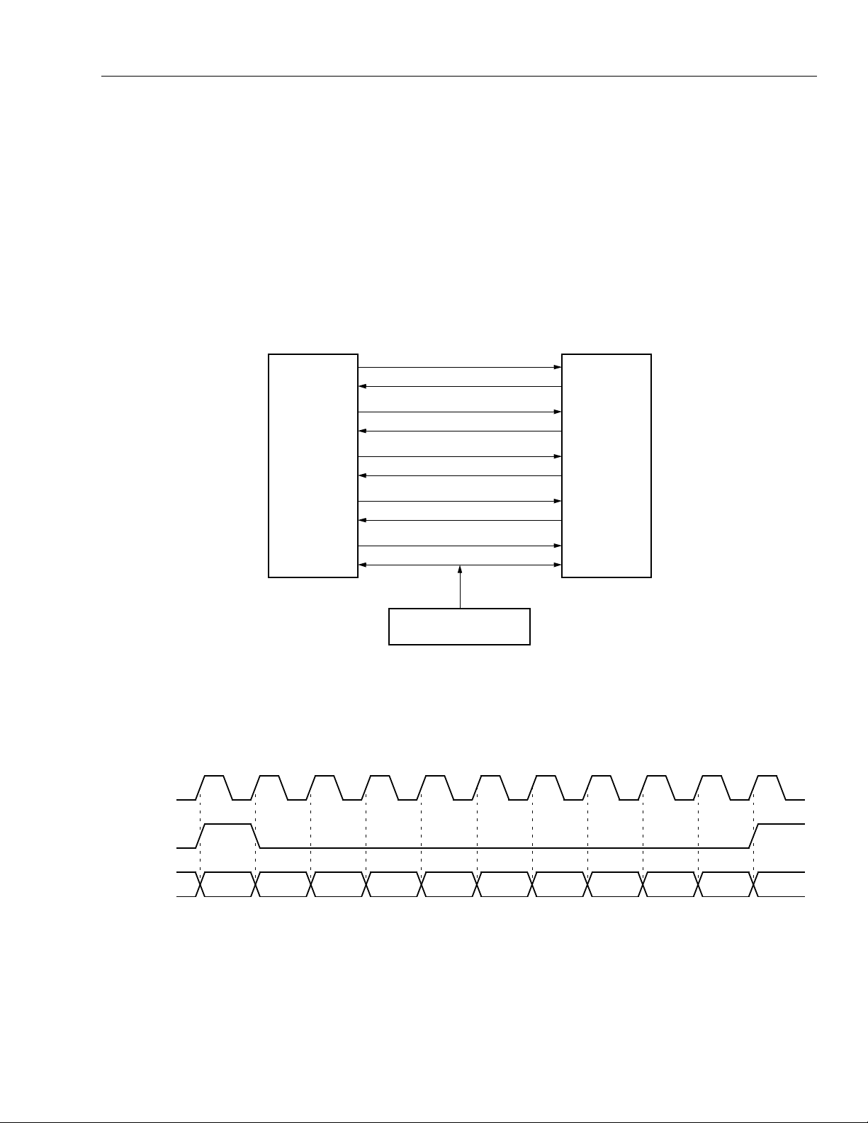
Reduced Media Independent Interface (RMII)
This interface reduces the interconnect circuits
between a MAC and PHY. In switch applications, this
protocol helps to reduce the pin count on the switch
ASIC significantly. A regular 16-pin MII reduces to a
7-pin (8-pin with an optional RXER pin) RMII. The
interconnect circuits are the following:
1. REF_CLK: A 50 MHz clock.
2. TX_EN.
3. TXD[1:0].
4. RXD[1:0].
5. CRS_D V.
6. RXER: Mandator
switch.
for the PHY, but optional for the
MII MAC I/F TO RMII MAC I/F
TXEN
TXD[3:0]
TXER
TXCLK
COL
CRS
RXDV
RXD[3:0]
RXER
RXCLK
MAC RMII PHY
RMII PHY I/F TO MII PHY I/F
TXEN
TXD[1:0]
CRS_DV
RXD[1:0]
RXER
REFCLK
50 MHz
Figure 4. Functional Description
TXEN
TXD[3:0]
TXER
TXCLK
COL
CRS
RXDV
RXD[3:0]
RXER
RXCLK
5-7505(F).r1
Lucent Technologies Inc. 13
Page 14
LU3X34FTR Preliminary Data Sheet
Quad 3 V 10/100 Ethernet Transceiver TX/FX July 2000
Functional Description
(continued)
Transmit Data Path
The PHY uses the 50 MHz REF_CLK as its reference
so that TXC (at the internal MII) and REF_CLK maintain a phase relationship. This helps to avoid elasticity
buffers on the transmit side. On the rising edge of
REF_CLK, 2-bit data is provided on the RMII TXD[1:0]
when TXEN is high. TXD[1:0] will be 00 to indicate idle
when TXEN is deasserted.
TX 10 Mbits/s Mode
The REF_CLK frequency is ten times the data rate in
this mode; therefore, the value on TXD[1:0] will be valid
such that TXD[1:0] may be sampled every tenth cycle,
regardless of the starting cycle within the group.
TX 100 Mbits/s Mode
There will be valid data on TXD[1:0] for each REF_CLK
period when TXEN is asserted.
Receive Data Path
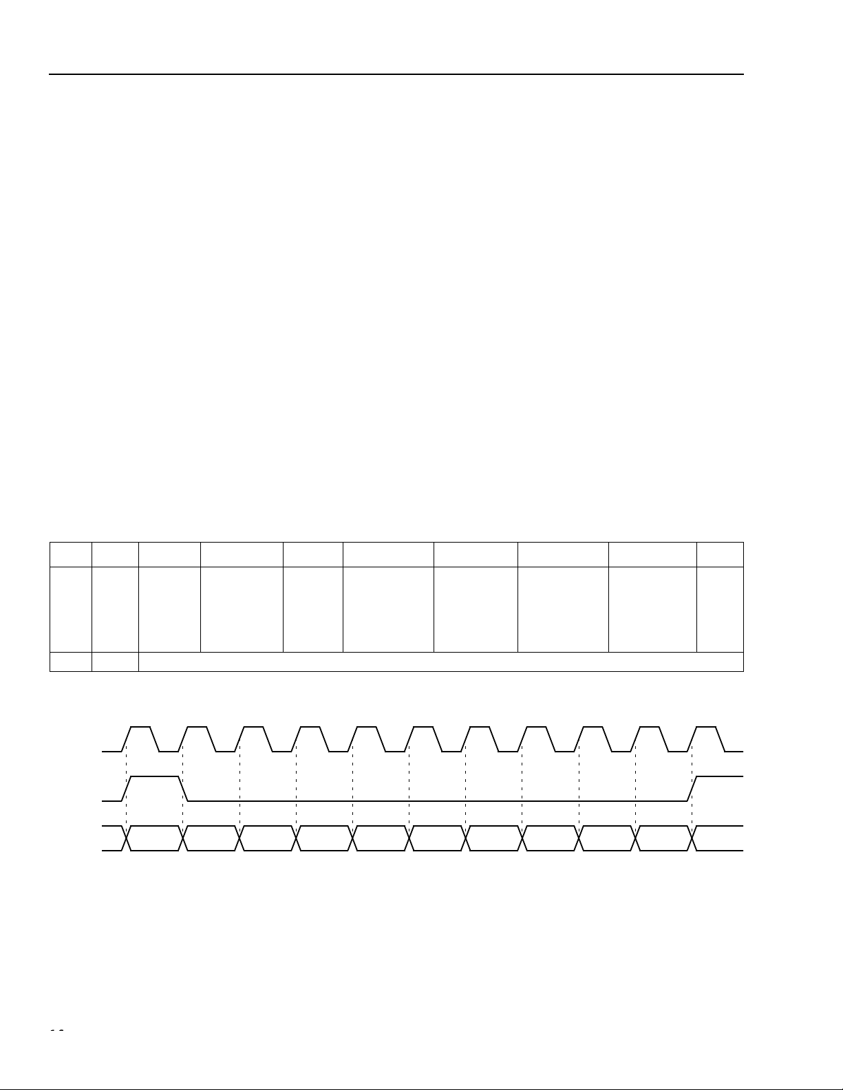
RXCLK (at the internal MII) is derived from the incoming data and, hence, does not maintain a phase relationship with REF_CLK. Therefore, an elasticity buffer
is required on the receive path. An 8-nibble deep elasticity buffer is required based on the ppm variation of
the clocks. CRS_DV is asserted asynchronously. Preamble is output onto the RMII once the internal signal
RX_DV is asserted (on the rising edge of the
REF_CLK). CRS_DV is deasserted asynchronously
with the fall of RX_DV, but CRS_DV keeps toggling as
long as data is being flushed out of the elasticity buffer.
RX 10 Mbits/s Mode
After the assertion of CRS_DV, the receive data signals, RXD[1:0], will be 00 until the 10Base-T PHY has
recovered the clock and decoded the receive data.
Since REF_CLK is 10 times the data rate in this mode,
the value on RXD[1:0] will be valid such that it can be
sampled every tenth cycle, regardless of the starting
cycle within the group.
RX 100 Mbits/s Mode
After the assertion of CRS_DV, the receive data signals, RXD[1:0] will be 00 until the start-of-stream (SSD)
delimiter has been detected.
Collision Detection
The RMII does not have a collision signal, so all collisions are detected internal to the MAC. This is an AND
function of TXEN and CRS derived from CRS_DV.
CRS_DV cannot be directly ANDed with TXEN,
because CRS_DV may toggle at the end of a frame to
provide separation between CRS and RXDV.
Receiver Error
The RX_ER signal is asserted for one or more
REF_CLK periods to indicate that an error was
detected within the current receive frame.
REF_CLK
CRS
RX_DV
CRS_DV
CRS
RMII_RXD[1:0] 00 01 01 00
5-7506(F).r2
Figure 5. RMII Receive Timing from Internal MII Signals
1414 Lucent Technologies Inc.
Page 15
Preliminary Data Sheet LU3X34FTR
July 2000 Quad 3 V 10/100 Ethernet Transceiver TX/FX
Functional Description
(continued)
Loopback
During normal operation, TXD[1:0] and TX_EN will not be looped back to CRS_DV and RXD[1:0].
Serial Media Independent Interface (SMII)
The SMII allows a further reduction in the number of signals that are required to interface a PHY to a MAC. There
are two global signals, CLK125 and SYNC, and two per-port signals, RXD, TXD. All signals are synchronous to the
125 MHz clock.
MULTI-MAC
SMII_TXD0
SMII_RXD0
SMII_TXD1
SMII_RXD1
SMII_TXD2
SMII_RXD2
SMII_TXD3
SMII_RXD3
LU3X34FTR
PORT 0
PORT 1
PORT 2
PORT 3
REF_CLK
SMII_SYNC
SMII_RXD
SMII_SYNC
REF_CLK
125 MHz
REFERENCE CLOCK
5-7507(F).r4
Figure 6. SMII Connection Diagram
1234567891011
CRS RXDV RXD0 RXD1 RXD2 RXD3 RXD4 RXD5 RXD6 RXD7
5-7507(F).r4
Figure 7. Receive Sequence Diagram
Lucent Technologies Inc. 15
Page 16
LU3X34FTR Preliminary Data Sheet
Quad 3 V 10/100 Ethernet Transceiver TX/FX July 2000
Functional Description
(continued)
Receive Path
Receive data and control information are signaled in
10-bit segments. These 10-bit boundaries are delimited
by the SYNC signal. The connected MAC should generate these SYNC pulses every ten clocks. In
100 Mbits/s mode, each segment represents a new
byte of data. In 10 Mbits/s mode, each segment is
repeated ten times, so every ten segments represents
a new byte of data.
The receive sequence contains all of the information
found on the standard MII receive path. RXD[7:0] convey packet data whenever the RXDV bit is set. During
an interframe gap, RXDV bit is set to 0 and RXD[7:0]
indicate receiver status. Bit RXD5 indicates the validity
of the upper nibble of the last byte of data of the previous frame. Bit RXD0 indicates an error detected by the
PHY in the previous frame. Both of these bits will be
valid in the segment immediately following a frame, and
will remain valid until the first data segment of the next
frame.
Transmit Data Path
Transmit data and control information are signaled in
10-bit segments similar to the receive path. These
10-bit boundaries are delimited by the SYNC signal.
The connected MAC should generate these SYNC
pulses every ten clocks. In 100 Mbits/s mode, each
new segment represents a new byte of data. In
10 Mbits/s mode, each segment is repeated ten times;
therefore, ev ery ten segments represents a new byte of
data. The PHY can sample one of every ten segments.
The PHY is concerned only with packet data, so there
is no status information passed from the MAC to the
PHY during the interframe gap; this is unlike the
receive side.
Collision Detection
The PHY does not directly indicate that a collision has
occurred. It is left up to the MAC to detect the assertion
of both CRS and TXEN.
Table 10. Receive Data/Status Encoding
CRS RXDV RXD0 RXD1 RXD2 RXD3 RXD4 RXD5 RXD6 RXD7
X0Rcvr
error in
the pre-
10 Mbits/s
vious
frame.
100 Mbits/s
Speed:
0 =
1 =
Duplex:
0 = half
1 = full
Link:
0 = no link
1 = good link
Jabber:
0 = OK
1 = detected
Upper nibble:
0 = invalid
1 = valid
False carrier:
0 = OK
1 = detected
X 1 One Data Byte (two MII nibbles)
1234567891011
SMII_CLK
SYNC
TXD
TXER TXEN TXD0 TXD1 TXD2 TXD3 TXD4 TXD5 TXD6 TXD7
5-7508(F).r1
Figure 8. Transmit Sequence Diagram
1
1616 Lucent Technologies Inc.
Page 17

Preliminary Data Sheet LU3X34FTR
July 2000 Quad 3 V 10/100 Ethernet Transceiver TX/FX
Functional Description
(continued)
Media Independent Interface (MII)—Internal
The LU3X34FTR implements
compliant MII interface which connects to the MII-RMII
module. This module converts the 4-bit MII receive
data to 2-bit RMII receive data. Similarly, it conv erts the
2-bit RMII transmit data (received from the MAC) to
4-bit MII transmit data. The following describes the
internal MII functions.
Transmit Data Interface
Each internal MII transmit data interface comprises
seven signals: TXD[3:0] are the nibble size data path,
TXEN signals the presence of data on TXD, TXER indicates substitution of data with the HALT symbol, and
TXCLK carries the transmit clock that synchronizes all
the transmit signals. TXCLK is usually supplied by the
on-chip clock synthesizer.
Receive Data Interface
Each internal MII receive data interface also comprises
seven signals: RXD[3:0] are the nibble size data path,
RXDV signals the presence of data on RXD, RXER
indicates the validity of data, and RXCLK carries the
receive clock. Depending upon the operation mode,
RXCLK signal is generated by the clock recovery module of either the 100Base-X or 10Base-T receiver.
Status Interface
Two internal MII status signals, COL and CRS, are generated in each of the four channels to indicate collision
status and carrier sense status. COL is asserted asynchronously whenever the respective channel of
LU3X34FTR is transmitting and receiving at the same
time in a half-duplex operation mode. CRS is asserted
asynchronously whenever there is activity on either the
transmitter or the receiver. In repeater or full-duplex
mode, CRS is asserted only when there is activity on
the receiver.
Operation Modes
Each channel of the LU3X34FTR supports two operation modes and an isolate mode as described below.
100 Mbits/s Mode
internal MII operates in nibble mode with a clock rate of
25 MHz. In normal operation, the internal MII data at
RXD[3:0] and TXD[3:0] are 4 bits wide.
10 Mbits/s Mode
tion, the TXCLK and RXCLK operate at 2.5 MHz. The
. For 100 Mbits/s operation, the
. For 10 Mbits/s nibble mode opera-
IEEE
802.3u Clause 22
data paths are 4 bits wide using TXD[3:0] and
RXD[3:0] signal lines.
MII Isolate Mode
isolate mode that is controlled by bit 10 of each one of
the four control registers (register 0h). At reset,
LU3X34FTR will initialize this bit to the logic level transition of the ISOLA TE pin. Setting the bit to a 1 will also
put the port in MII isolate mode.
When in isolate mode, the specified port on the
LU3X34FTR does not respond to packet data present
at TXD[3:0], TXEN, and TXER inputs and presents a
high impedance on the TXCLK, RXCLK, RXDV, RXER,
RXD[3:0], COL, and CRS outputs. The LU3X34FTR
will continue to respond to all management transactions while the PHY is in isolate mode.
Serial Management Interface (SMI)
The serial management interface is used to obtain status and to configure the PHY. This mechanism corresponds to the MII specifications for 100Base-X (Clause
22), and supports registers 0 through 6. Additional vendor-specific registers are implemented within the range
of 16 to 31. All the registers are described in the MII
Registers section.
Management Register Access
The SMI consists of two pins, management data clock
(MDC) and management data input/output (MDIO).
The LU3X34FTR is designed to support an MDC frequency specified in the
2.5 MHz. The MDIO line is bidirectional and may be
shared by up to 32 devices.
The MDIO pin requires a 1.5 kΩ pull-up resistor which,
during idle and turnaround periods, will pull MDIO to a
logic one state. Each MII management data frame is
64 bits long. The first 32 bits are preamble consisting of
32 contiguous logic one bits on MDIO and 32 corresponding cycles on MDC. Following preamble is the
start-of-frame field indicated by a <01> pattern. The
next field signals the operation code (OP): <10> indicates read from MII management register operation,
and <01> indicates write to MII management register
operation. The next two fields are PHY device address
and MII management register address. Both of them
are 5 bits wide, and the most significant bit is transferred first.
During read operation, a 2-bit turnaround (TA) time
spacing between the register address field and data
field is provided for the MDIO to avoid contention. Following the turnaround time, a 16-bit data stream is read
from or written into the MII management registers of
the LU3X34FTR.
. The LU3X34FTR implements an MII
IEEE
specification of up to
Lucent Technologies Inc. 17
Page 18

LU3X34FTR Preliminary Data Sheet
Quad 3 V 10/100 Ethernet Transceiver TX/FX July 2000
Functional Description
The LU3X34FTR supports a preamble suppression
mode as indicated by a 1 in bit 6 of the basic mode status register (BMSR, address 01h). If the station management entity (i.e., MAC or other management
controller) determines that all PHYs in the system support preamble suppression by reading a 1 in this bit,
then the station management entity need not generate
preamble for each management transaction. The
LU3X34FTR requires a single initialization sequence of
32 bits of preamble following powerup/hardware reset.
This requirement is generally met by the mandatory
pull-up resistor on MDIO or the management access
made to determine whether preamble suppression is
supported. While the LU3X34FTR will respond to management accesses without preamble, a minimum of
one idle bit between management transactions is
required as specified in
The PHY device address is stored in bits [4:0] of the
PHY address register (register address 19h). During
powerup or hardware reset, the upper 3 bits of this field
IEEE
(continued)
802.3u.
are initialized by the three I/O pins designated as
PHY[4:2] and can be subsequently changed by writing
into this register address (19h). The lower 2 bits are initialized to 00, and represent the PHY address for port
1. All subsequent ports have their PHY address increment from this base address (i.e., PHY address for port
1 = 10h, PHY address for port 2 = 11h, PHY address
for port 3 = 12h, PHY address for port 4 = 13h).
MDIO Interrupt
The LU3X34FTR implements interrupt capability that
can be used to notify the management station of certain events. Interrupt requested by any of the four PHYs
is combined in this pin. It generates an active-low interrupt pulse of 80 ns wide on the INTZ output pin whenever one of the interrupt status registers (register
address 1Eh) becomes set while its corresponding
interrupt mask register (register address 1Dh) is unmasked. Reading the interrupt status register (register
1Eh) shows the source of the interrupt and clears the
interrupt output signal.
18 Lucent Technologies Inc.
Page 19

Preliminary Data Sheet LU3X34FTR
July 2000 Quad 3 V 10/100 Ethernet Transceiver TX/FX
Functional Description
(continued)
100Base-X Module
The LU3X34FTR implements 100Base-X compliant PCS and PMA and 100Base-TX compliant TP-PMD as illustrated in Figure 9. Bypass options for each of the major functional blocks within the 100Base-X PCS provides flexibility for various applications. 100 Mbits/s PHY loopback is included for diagnostic purposes.
RXD[1:0]
CRS_DV
REF_CLK
MII-TO-RMII/SMII CONVERSION
RXCLK
RXD[3:0]
BYP_ALIGN
CRS
RXDV
RXEN
4B/5B
DECODE
BYP_4B5B
RX STATE MACHINE
DESCRAMBLER
RYP_SCR
100BASE-X RECEIVER
SERIAL-TO-PARALLEL
CLOCK RECOVERY
100M PHY LOOPBACK
FORX±
FOSD±
EQUALIZER
TPRX±
TXEN
TXD[1:0]
RMII/SMII-TO-MII CONVERSION
COL
TXCLK
TXEN
TXER
BYP_4B5B BYP_SCR
TXD[3:0]
4B/5B DECODE
TX STATE MACHINE
BYP_ALIGN MLI-3
SCRAMBLER
STATE
MACHINE
PARALLEL-TO-SERIAL
100BASE-X TRANSMITTER
10/100
TX
DRIVER
FIBER
OPTIC
DRIVER
TPTX±
FOTX±
5-7519(F)
Figure 9. 100Base-X Data Path
Lucent Technologies Inc. 19
Page 20

LU3X34FTR Preliminary Data Sheet
Quad 3 V 10/100 Ethernet Transceiver TX/FX July 2000
Functional Description
(continued)
100Base-X Transmitter
The 100Base-X transmitter consists of functional
blocks which convert synchronous 4-bit nibble data, as
provided by the internal MII, to a 125 Mbits/s serial
data stream. This data stream may be routed either to
the on-chip twisted-pair PMD for 100Base-TX signaling, or to an external fiber-optic PMD for 100Base-FX
applications. The LU3X34FTR implements the
100Base-X transmit state machine as specified in the
IEEE
802.3u Standard, Clause 24 and comprises the
following functional blocks in its data path:
■
Symbol encoder.
■
Scrambler block.
■
Parallel/serial converter and NRZ/NRZI encoder
block.
Symbol Encoder
The symbol encoder converts 4-bit (4B) nibble data
generated by the RMII-MII module into 5-bit (5B) symbols for transmission. This conversion is required to
allow control symbols to be combined with data symbols. Refer to Table 11 for 4B to 5B symbol mapping.
Following onset of the TXEN signal, the 4B/5B symbol
encoder replaces the first two nibbles of the preamble
from the MAC frame with a /J/K code-group pair (11000
10001) start-of-stream delimiter (SSD). The symbol
encoder then replaces subsequent 4B codes with corresponding 5B symbols. Following negation of the
TXEN signal, the encoder substitutes the first two idle
symbols with a /T/R code-group pair (01101 00111)
end-of-stream delimiter (ESD) then continuously injects
idle symbols into the transmit data stream until the next
transmit packet is detected.
20 Lucent Technologies Inc.
Page 21

Preliminary Data Sheet LU3X34FTR
July 2000 Quad 3 V 10/100 Ethernet Transceiver TX/FX
Functional Description
Table 11. Symbol Code Scrambler
Symbol
Name
0 11110 0000 Data 0.
1 01001 0001 Data 1.
2 10100 0010 Data 2.
3 10101 0011 Data 3.
4 01010 0100 Data 4.
5 01011 0101 Data 5.
6 01110 0110 Data 6.
7 01111 0111 Data 7.
8 10010 1000 Data 8.
9 10011 1001 Data 9.
A 10110 1010 Data A.
B 10111 1011 Data B.
C 11010 1100 Data C.
D 11011 1101 Data D.
E 11100 1110 Data E.
F 11101 1111 Data F.
I 11111 undefined Idle: interstream fill code.
J 11000 0101 First start-of-stream delimiter.
K 10001 0101 Second start-of-stream delimiter.
T 01101 undefined First end-of-stream delimiter.
R 00111 undefined Second end-of-stream delimiter.
H 00100 undefined Halt: transfer error.
V 00000 undefined Invalid code.
V 00001 undefined Invalid code.
V 00010 undefined Invalid code.
V 00011 undefined Invalid code.
V 00101 undefined Invalid code.
V 00110 undefined Invalid code.
V 01000 undefined Invalid code.
V 01100 undefined Invalid code.
V 10000 undefined Invalid code.
V 11001 undefined Invalid code.
5B Code
[4:0]
(continued)
4B Code
[3:0]
Interpretation
Lucent Technologies Inc. 21
Page 22

LU3X34FTR Preliminary Data Sheet
Quad 3 V 10/100 Ethernet Transceiver TX/FX July 2000
Functional Description
(continued)
Scrambler Block
For 100Base-TX applications, the scrambler is required
to control the radiated emissions at the media connector and on the twisted-pair cable.
The LU3X34FTR implements a data scrambler as
defined by the TP-PMD stream cipher function. The
scrambler uses an 11-bit ciphering linear feedback shift
register (LFSR) with the following recursive linear function:
X[n] = X[n – 11] + X[n – 9] (modulo 2)
The output of the LFSR is combined with data from the
encoder via an exclusive-OR logic function. By scrambling the data, the total energy launched onto the cable
is randomly distributed over a wide frequency range.
A seed value for the scrambler function can be loaded
by setting bit 4 of register 18h. When this bit is set, the
contents of bits [10:0] of register 19h (that are composed of the 5-bit PHY address and a 6-bit user seed)
will be loaded into the LFSR. By specifying unique
seed value for each PHY in a system, the total EMI
energy produced by a repeater application can be
reduced.
Parallel-to-Serial and NRZ-to-NRZI Conversion
After the transmit data stream is scrambled, data is
loaded into a shift register and clocked out with a
125 MHz clock into a serial bit stream. The serialized
data is further converted from NRZ-to-NRZI format,
which produces a transition on every logic one and no
transition on logic zero.
125 Mbits/s receive data stream may originate from the
on-chip twisted-pair transceiver in a 100Base-TX application. Alternatively, the receive data stream may be
generated by an external optical receiver as in a
100Base-FX application.
The receiver block consists of the following functional
blocks:
■
Equalizer.
■
Clock recovery module.
■
NRZI/NRZ and serial/parallel decoder.
■
Descrambler.
■
Symbol alignment block.
■
Symbol decoder.
■
Collision detect block.
■
Carrier sense block.
■
Stream decoder block.
Clock Recovery
The clock recovery module accepts 125 Mbits/s scrambled NRZI data stream from either the on-chip
100Base-TX receiver or from an external 100Base-FX
transceiver. The LU3X34FTR uses an onboard digital
phase-locked loop (PLL) to extract clock information of
the incoming NRZI data, which is then used to retime
the data stream and set data boundaries.
After power-on or reset, the PLL locks to a free-running
25 MHz clock derived from the external clock source.
When initial lock is achieved, the PLL switches to lock
to the data stream, extracts a 125 MHz clock from the
data, and uses it for bit framing of the recovered data.
Collision Detect
During 100 Mbits/s half-duplex operation, collision condition is detected if the transmitter and receiver become
active simultaneously. Collision detection is indicated
NRZI-to-NRZ and Serial-to-Parallel Conversion
The recovered data is converted from NRZI to NRZ.
The data is not necessarily aligned to 4B/5B codegroup’s boundary.
by the COL signal of the internal MII. For full-duplex
applications, the COL signal is never asserted.
100Base-X Receiver
Data Descrambling
The descrambler acquires synchronization with the
data stream by recognizing idle bursts of 40 or more
The 100Base-X receiver consists of functional blocks
required to recover and condition the 125 Mbits/s
receive data stream. The LU3X34FTR implements the
100Base-X receive state machine diagram as given in
ANSI/
IEEE
Standard 802.3u, Clause 24. The
bits and locking its deciphering linear feedback shift
register (LFSR) to the state of the scrambling LFSR.
Upon achieving synchronization, the incoming data is
XORed by the deciphering LFSR and descrambled.
22 Lucent Technologies Inc.
Page 23

Preliminary Data Sheet LU3X34FTR
July 2000 Quad 3 V 10/100 Ethernet Transceiver TX/FX
Functional Description
In order to maintain synchronization, the descrambler
continuously monitors the validity of the unscrambled
data that it generates. To ensure this, a link state monitor and a hold timer are used to constantly monitor the
synchronization status. Upon synchronization of the
descrambler, the hold timer starts a 722 µs countdown.
Upon detection of sufficient idle symbols within the
722 µs period, the hold timer will reset and begin a new
countdown. This monitoring operation will continue
indefinitely given a properly operating network connection with good signal integrity. If the link state monitor
does not recognize sufficient unscrambled idle symbols
within the 722 µs period, the desc ramb le r will be f or ced
out of the current state of synchronization and reset in
order to reacquire synchronization. Register 18h, bit 3,
can be used to extend the timer to 2 ms.
Symbol Alignment
The symbol alignment circuit in the LU3X34FTR determines code word alignment by recognizing the /J/K
delimiter pair. This circuit operates on unaligned data
from the descrambler. Once the /J/K symbol pair
(11000 10001) is detected, subsequent data is aligned
on a fixed boundary.
Symbol Decoding
The symbol decoder functions as a look-up table that
translates incoming 5B symbols into 4B nibbles. The
symbol decoder first detects the /J/K symbol pair preceded by idle symbols and replaces the symbol with
MAC preamble. All subsequent 5B symbols are converted to the corresponding 4B nibbles for the duration
of the entire packet. This conversion ceases upon the
detection of the /T/R symbol pair denoting the end-ofstream delimiter (ESD). The translated data is presented on the RXD[3:0] signal lines with RXD[0] represents the least significant bit of the translated nibble.
Valid Data Signal
The valid data signal (RXDV) indicates that recovered
and decoded nibbles are being presented on the
RXD[3:0] outputs synchronous to RXCLK. RXDV is
asserted when the first nibble of translated /J/K is
ready for transfer ov er the internal MII. It remains active
until either the /T/R delimiter is recognized, link test
indicates failure, or no signal is detected. On any of
these conditions, RXDV is deasserted.
Receiver Errors
The RXER signal is used to communicate receiver
error conditions. While the receiver is in a state of hold-
(continued)
ing RXDV asserted, the RXER will be asserted for each
code word that does not map to a valid code-group.
100Base-X Link Monitor
The 100Base-X link monitor function allows the
receiver to ensure that reliable data is being received.
Without reliable data reception, the link monitor will halt
both transmit and receive operations until such time
that a valid link is detected.
The LU3X34FTR performs the link integrity test as outlined in
diagram. The link status is multiplexed with 10 Mbits/s
link status to form the reportable link status bit in serial
management register 1 and driven to the LNKLED
pins.
When persistent signal energy is detected on the network, the logic moves into a link-ready state after
approximately 500 µs and waits for an enable from the
autonegotiation module. When received, the link-up
state is entered, and the transmit and receive logic
blocks become active. Should autonegotiation be disabled, the link integrity logic moves immediately to the
link-up state after entering the link-ready state.
Carrier Sense
Carrier sense (CRS) for 100 Mbits/s operation is
asserted upon the detection of two noncontiguous
zeros occurring within any 10-bit boundary of the
receive data stream.
The carrier sense function is independent of symbol
alignment. In switch mode, CRS is asserted during
either packet transmission or reception. For repeater
mode, CRS is asserted only during packet reception.
When the idle symbol pair is detected in the receive
data stream, CRS is deasserted. In repeater mode,
CRS is only asserted due to receive activity. CRS is
intended to encapsulate RXDV.
Bad SSD Detection
A bad start-of-stream delimiter (bad SSD) is an error
condition that occurs in the 100Base-X receiver if carrier is detected (CRS asserted) and a valid /J/K set of
code-groups (SSD) is not received.
If this condition is detected, then the LU3X34FTR will
assert RXER and present RXD[3:0] = 1110 to the internal MII for the cycles that correspond to received 5B
code-groups until at least two idle code-groups are
detected. In addition, the false carrier counter (address
13h) will be incremented by one. Once at least two idle
code-groups are detected, RXER and CRS become
deasserted.
IEEE
100Base-X (Clause 24) link monitor state
Lucent Technologies Inc. 23
Page 24

LU3X34FTR Preliminary Data Sheet
Quad 3 V 10/100 Ethernet Transceiver TX/FX July 2000
Functional Description
Far-End Fault Indication
Autonegotiation provides a mechanism for transferring
information from the local station to the link partner that
a remote fault has occurred for 100Base-TX. As autonegotiation is not currently specified for operation over
fiber, the far-end fault indication function (FEFI) provides this capability for 100Base-FX applications.
A remote fault is an error in the link that one station can
detect while the other cannot. An example of this is a
disconnected wire at a station’s transmitter . This station
will be receiving valid data and detect that the link is
good via the link integrity monitor, but will not be able to
detect that its transmission is not propagating to the
other station.
A 100Base-FX station that detects such a remote fault
may modify its transmitted idle stream from all ones to
a group of 84 ones followed by a single 0. This is
referred to as the FEFI idle pattern.
The FEFI function is controlled by bit 11 of register 18h.
It is initialized to 1 (enabled) if the FOSEL pin is at logic
high level during powerup or reset. If the FEFI function
is enabled, the LU3X34FTR will halt all current operations and transmit the FEFI idle pattern when FOSD
signal is deasserted following a good link indication
from the link integrity monitor. FOSD signal is generated internally from the FORX± circuit. Transmissi on of
the FEFI idle pattern will continue until FORX± signal is
asserted. If three or more FEFI idle patterns are
detected by the LU3X34FTR, then bit 4 of the basic
mode status register (address 01h) is set to one until
read by management. Additionally, upon detection of
far-end fault, all receive and transmit MII activity is disabled/ignored.
(continued)
100Base-TX Transceiver
LU3X34FTR implements a TP-PMD compliant transceiver for 100Base-TX operation. The differential transmit driver is shared by the 10Base-T and 100Base-TX
subsystems. This arrangement results in one device
that uses the same external magnetics for both the
10Base-T and the 100Base-TX transmission with simple RC component connections. The individually waveshaped 10Base-T and 100Base-TX transmit signals
are multiplexed in the transmit output driver section.
Transmit Drivers
The LU3X34FTR 100Base-TX transmit driver implements MLT-3 translation and wave-shaping functions.
The rise/fall time of the output signal is closely controlled to conform to the target range specified in the
ANSI TP-PMD standard.
Twisted-Pair Receiver
For 100Base-TX operation, the incoming signal is
detected by the on-chip twisted-pair receiver that comprises the differential line receiver, an adaptive equalizer, and baseline wander compensation circuits.
The LU3X34FTR uses an adaptive equalizer which
changes filter frequency response in accordance with
cable length. The cable length is estimated based on
the incoming signal strength. The equalizer tunes itself
automatically for any cable length to compensate for
the amplitude and phase distortions incurred from the
cable.
24 Lucent Technologies Inc.
Page 25

Preliminary Data Sheet LU3X34FTR
July 2000 Quad 3 V 10/100 Ethernet Transceiver TX/FX
Functional Description
(continued)
10Base-T Module
The 10Base-T transceiver module is
pliant. It includes the receiver, tr ansmitter, collision,
heartbeat, loopback, jabber, waveshaper, and link
integrity functions, as defined in the standard. Figure 10
provides an overview for the 10Base-T module.
TPRX±
RECEIVE
FILTER
FILTER
IEEE
SMART
SQUELCH
802.3 com-
CLOCK
RECOVERY
The LU3X34FTR 10Base-T module is comprised of
the following functional blocks:
■
Manchester encoder and decoder.
■
Collision detector.
■
Link test function.
■
Transmit driver and receiver.
■
Serial and parallel interface.
■
Jabber and SQE test functions.
■
Polarity detection and correction.
RXCLK
CRS_DV
RXD[1:0]
REF_CLK
10BASE-T
RECEIVE
PCS
CRS
RXD[3:0]
RXDV
COL
MII-TO-RMII/SMII
CONVERTER
TPTX±
10/100
TX DRIVER
WAVE
SHAPER
10BASE-T
RECEIVE
PCS
TXD[3:0]
TXCLK
Figure 10. 10Base-T Module Data Path
TXEN
TXER
RMII/SMII-TO-MII
CONVERTER
TXEN
TXD[1:0]
TXCLK
5-7521(F)
Lucent Technologies Inc. 25
Page 26

LU3X34FTR Preliminary Data Sheet
Quad 3 V 10/100 Ethernet Transceiver TX/FX July 2000
Functional Description
Operation Modes
The LU3X34FTR 10Base-T module is capable of operating in either half-duplex mode or full-duplex mode. In
half-duplex mode, the LU3X34FTR functions as an
IEEE
802.3 compliant transceiver with fully integrated
filtering. The COL signal is asserted during collisions or
jabber events, and the CRS signal is asserted during
transmit and receive. In full-duplex mode, the
LU3X34FTR can simultaneously transmit and receive
data.
Manchester Encoder/Decoder.
transmission begins when the transmit enable input
(TXEN) goes high and continues as long as the transceiver is in good link state. Transmission ends when the
transmit enable input goes low. The last transition
occurs at the center of the bit cell if the last bit is a 1, or
at the boundary of the bit cell if the last bit is 0.
Decoding is accomplished by a differential input
receiver circuit and a phase-locked loop that separates
the Manchester-encoded data stream into clock signals
and NRZ data. The decoder detects the end of a frame
when no more midbit transitions are detected. Within
one and a half bit times after the last bit, carrier sense
is deasserted.
Transmit Driver and Receiver.
grates all the required signal conditioning functions in
its 10Base-T block such that external filters are not
required. Only an isolation transformer and impedancematching resistors are needed for the 10Base-T transmit and receive interface. The internal transmit filtering
ensures that all the harmonics in the transmit signal are
attenuated properly.
Smart Squelch.
ble for determining when valid data is present on the
differential receive. The LU3X34FTR implements an
intelligent receive squelch on the TPRX+/– differential
inputs to ensure that impulse noise on the receive
inputs will not be mistaken for a valid signal. The
squelch circuitry employs a combination of amplitude
and timing measurements (as specified in the
802.3 10Base-T standard) to determine the validity of
data on the twisted-pair inputs.
The signal at the start of the packet is checked by the
analog squelch circuit and any pulses not exceeding
the squelch level (either positive or negative, depending upon polarity) will be rejected. Once this first
squelch level is overcome correctly, the opposite
squelch level must then be exceeded within 150 ns.
Finally, the signal must exceed the original squelch
level within an additional 150 ns to ensure that the input
waveform will not be rejected.
The smart squelch circuit is responsi-
(continued)
Data encoding and
The LU3X34FTR inte-
IEEE
Only after all of these conditions have been satisfied
will a control signal be generated to indicate to the
remainder of the circuitry that valid data is present.
V alid data is considered to be present until the squelch
level has not been generated for a time longer than
200 ns, indicating end of packet. Once good data has
been detected, the squelch levels are reduced to minimize the effect of noise, causing premature end-ofpacket detection. The receive squelch threshold level
can be lowered for use in longer cable applications.
This is achieved by setting bit 11 of register address
1Ah.
Carrier Sense.
receive activity once valid data is detected via the
smart squelch function.
For 10 Mbits/s half-duplex operation, CRS is asserted
during either packet transmission or reception.
For 10 Mbits/s full-duplex operation, the CRS is
asserted only due to receive activity.
In repeater mode, CRS is only asserted due to receive
activity. CRS is deasserted following an end of packet.
Collision Detection.
sion pin. Collision is detected internal to the MAC,
which is generated by an AND function of TXEN and
CRS derived from CRS_DV. CRS_DV cannot be
directly ANDed with TXEN because CRS_DV may toggle at the end of a frame to provide separation between
CRS and RXDV. The internal MII will still generate the
COL signal, but this information is not passed to the
MAC via the RMII.
Jabber Function.
LU3X34FTR's output and disables the transmitter if it
attempts to transmit a longer than legal-sized packet. If
TXEN is high for greater than 24 ms, the 10Base-T
transmitter will be disabled. Once disabled by the jabber function, the transmitter stays disabled for the
entire time that the TXEN signal is asserted. This signal has to be deasserted for approximately 256 ms (the
unjab time) before the jabber function re-enables the
transmit outputs. The jabber function can be disabled
by setting bit 10 of register 1Ah.
Link Test Function.
integrity of the connection with the remote end. If valid
link pulses are not received, the link detector disables
the 10Base-T twisted-pair transmitter, receiver, and collision detection functions.
The link pulse generator produces pulses as defined in
the
IEEE
802.3 10Base-T standard. Each link pulse is
nominally 100 ns in duration and is transmitted every
16 ms, in the absence of transmit data.
Carrier sens e (CRS ) is as serted due to
The RMII does not have a colli-
The jabber function monitors the
A link pulse is used to check the
26 Lucent Technologies Inc.
Page 27

Preliminary Data Sheet LU3X34FTR
July 2000 Quad 3 V 10/100 Ethernet Transceiver TX/FX
Functional Description
Automatic Link Polarity Detection.
LU3X34FTR's 10Base-T transceiver module incorporates an automatic link polarity detection circuit. The
inverted polarity is determined when seven consecutive
link pulses of inverted polarity or three consecutive
packets are received with inverted end-of-packet
pulses. If the input polarity is reversed, the error condition will be automatically corrected and reported in
bit 15 of register 1Ch.
The automatic link polarity detection function can be
disabled by setting bit 3 of register 1Ah.
Clock Synthesizer
The LU3X34FTR implements a clock synthesizer that
generates all the reference clocks needed from a single
external frequency source. The clock source must be a
TTL level signal at 25 MHz ± 50 ppm.
Autonegotiation
The autonegotiation function provides a mechanism for
exchanging configuration information between two
ends of a link segment and automatically selecting the
highest-performance mode of operation supported by
both devices. Fast link pulse (FLP) bursts provide the
signaling used to communicate autonegotiation abilities
between two devices at each end of a link segment. For
further detail regarding autonegotiation, refer to
Clause 28 of the
LU3X34FTR supports four different Ethernet protocols,
so the inclusion of autonegotiation ensures that the
highest-performance protocol will be selected based on
the ability of the link partner.
The autonegotiation function within the LU3X34FTR
can be controlled either by internal register access or
by the use of configuration pins. At powerup and at
device reset, the configuration pins are sampled. If disabled, autonegotiation will not occur until software
enables bit 12 in register 0. If autonegotiation is
enabled, the negotiation process will commence immediately.
When autonegotiation is enabled, the LU3X34FTR
transmits the abilities programmed into the autonegotiation advertisement register at address 4h via FLP
bursts. Any combination of 10 Mbits/s, 100 Mbits/s,
half-duplex, and full-duplex modes may be selected.
Autonegotiation controls the exchange of configuration
information. Upon successful autonegotiation, the abilities reported by the link partner are stored in the autonegotiation link partner ability register at address 5h.
IEEE
802.3u specification. The
(continued)
The
The contents of the autonegotiation link partner ability
register are used to automatically configure to the
highest-performance protocol between the local and
far-end nodes. Software can determine which mode
has been configured by autonegotiation by comparing
the contents of register 04h and 05h and then selecting
the technology whose bit is set in both registers of highest priority relative to the following list.
1. 100Base-TX full duplex (highest priority).
2. 100Base-TX half duplex.
3. 10Base-T full duplex.
4. 10Base-T half duplex (lowest priority).
The basic mode control register at address 00h pr o-
vides control of enabling, disabling, and restarting of
the autonegotiation function. When autonegotiation is
disabled, the speed selection bit (bit 13) controls
switching between 10 Mbits/s or 100 Mbits/s operation,
while the duplex mode bit (bit 8) controls switching
between full-duplex operation and half-duplex operation. The speed selection and duplex mode bits have
no effect on the mode of operation when the autonegotiation enable bit (bit 12) is set.
The basic mode status register at address 01h indicates the set of available abilities for technology types
(bits 15 to 11), autonegotiation ability (bit 3), and
extended register capability (bit 0). These bits are hardwired to indicate the full functionality of the
LU3X34FTR. The BMSR also provides status on:
1. Whether autonegotiation is comp lete (bit 5).
2. Whether the link partner is advertising that a remote
fault has occurred (bit 4).
3. Whether a valid link has been established (bit 2).
The autonegotiation advertisement register at address
04h indicates the autonegotiation abilities to be advertised by the LU3X34FTR. All available abilities are
transmitted by default, but any ability can be suppressed by writing to this register or configuring external pins.
The autonegotiation link partner ability register at
address 05h indicates the abilities of the link partner as
indicated by autonegotiation communication. The contents of this register are considered valid when the
autonegotiation complete bit (bit 5, register address
01h) is set.
Lucent Technologies Inc. 27
Page 28

LU3X34FTR Preliminary Data Sheet
Quad 3 V 10/100 Ethernet Transceiver TX/FX July 2000
Functional Description
(continued)
Reset Operation
The LU3X34FTR can be reset either by hardware or
software. A hardware reset is accomplished by applying a negative pulse, with a duration of at least 1 ms to
the RSTZ pin of the LU3X34FTR during normal operation. A software reset is activated by setting the reset
bit in the basic mode control register (bit 15, register
00h). This bit is self-clearing and, when set, will return
a value of 1 until the software reset operation has completed.
Hardware reset operation samples the pins and initializes all registers to their default values. This process
includes re-evaluation of all hardware-configurable registers. A hardware reset affects all four PHYs in the
device.
A software reset can reset an individual PHY, and it
does not latch the external pins or reset the registers to
their respective default values.
Logic levels on several I/O pins are detected during a
hardware reset to determine the initial functionality of
LU3X34FTR. Some of these pins are used as output
ports after reset operation.
Care must be taken to ensure that the configuration
setup will not interfere with normal operation. Dedicated configuration pins can be tied to Vcc or ground
directly. Configuration pins multiplexed with logic level
output functions should be either weakly pulled up or
weakly pulled down through resistors. Configuration
pins multiplexed with LED outputs should be set up
with one of the following circuits shown in Figure 11.
The 10 kΩ resistor is required only for nondefault configuartion.
Pins ANEN, FD10, FD100, and HD100 have internal
pull-up resistors, making their default value a 1 without
any external components. Pins FOSEL, SMII_EN, and
PHYAD[2:4] have internal pull-down resistors, making
their default value a 0 without any external components.
Note:
The MDIO pin is pulled low during reset.
I/O PIN
Ω
10 k
I/O PIN
LOGIC 1 CONFIGURATION LOGIC 0 CONFIGURATION
10 k
Ω
5-6783(F).a
Figure 11. LED Configuration
PHY Address
The PHY device address is stored in bits [4:0] of the PHY address register (register address 19h). The upper 3 bits
of this field are initialized by the three I/O pins designated as PHY[4:2] during powerup or hardware reset and can
be changed afterward by writing into this register address (19h). The lower 2 bits are initialized to 00 and represent
the PHY address for port 0. The PHY address for all subsequent ports are increments from this base address (i.e.,
PHY address for port 0 = 10h, PHY address for port 1 = 11h, PHY address for port 2 = 12h, PHY address for
port 3 = 13h). These unique 5-bit addresses are used during serial management interface communication.
2828 Lucent Technologies Inc.
Page 29

Preliminary Data Sheet LU3X34FTR
July 2000 Quad 3 V 10/100 Ethernet Transceiver TX/FX
Functional Description
Autonegotiation and Speed Configuration
The four sets of five pins listed in Table 13 configure the speed capability of each channel of LU3X34FTR. The
logic state of these pins, at powerup or reset, is latched into the advertisement register (register address 04h) for
autonegotiation purposes. These pins are also used for evaluating the default value in the base mode control register (register 00h) according to Table 12.
Table 12. Autonego tiation
Configuration Pins at Reset Registers Initial Value
ANEN FD100
(bit 4.8)
01XXX 0 11
0011X0 11
0010X0 10
0001X0 01
00001 0 00
1XXXX 1 0 0
LED Configuration
The LU3X34FTR provides four LED output pins for each of its four ports. In addition to the default functions associated with their pin names, there are several registers that allow users to customize LED operations.
(continued)
HD100
(bit 4.7)
FD10
(bit 4.6)
HD10
(bit 4.5)
AUTONEG
reg 0.12
SPEED
reg 0.13
DUPLEX
reg 0.8
Register 11h (programmable LED register) at PHY address 2 implements even more flexible LED configurations.
Register 11h at PHY address 4 controls all even-numbered ports, and register 11h at address 5 controls all oddnumbered ports. Via the programmable LED register, each of the LEDs may be configured to operate in one of the
following modes: link, speed, duplex, receive, transmit, solid when link is up and blinks during activity, remote fault,
and collision. Bits [0:3] in these registers allow the user to invert the on/off logic for each of these four programmable LEDs individually.
Note that all LED circuits are switched under the control of the programmable LED register whenever the content of
register 11h differs from its default value.
Register 17h implements more LED configuration functions. With these registers, unused LED can be individually
turned off to reduce power consumption.
Fiber Mode Select
A logic one level on pins FOSEL[0:3] sets each channel in fiber mode individually. These pins are latched during
reset operation.
MII Registers
The LU3X34FTR has four independent PHYs in it. Each PHY has its own identical set of registers as tabulated
below. The PHY address differentiates which PHY to be read or written into. The following tables of registers are
applicable to each register.
Lucent Technologies Inc. 29
Page 30

LU3X34FTR Preliminary Data Sheet
Quad 3 V 10/100 Ethernet Transceiver TX/FX July 2000
MII Registers
Table 13. MII Management Registers
Address Register Name Basic/Extended
0h Control Regist er B
1h Status Register B
2h—3h PHY Identifier Register E
4h Autonegotiation Advertisement Register E
5h Autonegotiation Link Partner Ability Register E
6h Autonegotiation Expansion Register E
7h—Fh
12h Isolate Counter E
13h False Carrier Counter E
15h Receive Error Counter E
17h PHY Control/Status Register E
18h Config 100 Register E
19h PHY Address Register E
1Ah Config 10 Register E
1Bh Status 100 Register E
1Ch Status 10 Register E
1Dh Interrupt Mask Register E
1Eh Interrupt Status Register E
IEEE
Reserved E
Legend:
RO Read only.
R/W Read and write capable.
SC Self-clearing.
LL Latching low, unlatch on read.
LH Latching high, unlatch on read.
COR Clear on read.
Table 14. Control Register (Register 0h)
Bit(s) Name Description R/W Default
15 Reset 1—PHY reset
0—Normal operation
Setting this bit initiates the software reset
function that resets the selected port,
except for the phase-locked loop circuit. It
will not relatch in all hardware configuration pin values, but it will set all registers to
their default values. The software reset
process takes 25 µs to complete. This bit,
which is self-clearing, returns a value of 1
until the reset process is complete.
R/W
SC
0h
30 Lucent Technologies Inc.
Page 31

Preliminary Data Sheet LU3X34FTR
July 2000 Quad 3 V 10/100 Ethernet Transceiver TX/FX
MII Registers
Table 14. Control Register (Register 0h)
Bit(s) Name Description R/W Default
14 Loopback 1—Enable loopback mode
13 Speed Selection 1—100 Mbits/s
12 Autonegotiation Enable 1—Enable autonegotiation process
11 Powerdown 1—Powerdown
10 Isolate 1—Isolate PHY from MII
(continued)
(continued)
0—Disable loopback mode
This bit controls the PHY loopback operation that isolates the network transmitter
outputs (TPTX+/– and FOTX+/–) and
routes the MII transmit data to the MII
receive data path. This function should
only be used when autonegotiation is disabled (bit 12 = 0). The specific PHY
(10Base-T or 100Base-X) used for this
operation is determined by bits 12 and 13
of this register.
0—10 Mbits/s
Link speed is selected by this bit or by
autonegotiation if bit 12 of this register is
set (in which case, the value of this bit is
ignored). At powerup or reset, this bit will
be set unless ANEN, FD100, and HD100
pins are all in logic low state.
0—Disable autonegotiation process
This bit determines whether the link speed
should be set up by the autonegotiation
process. It is set at powerup or reset if the
ANEN pin detects a logic 1 input level.
0—Normal operation
Setting this bit puts the LU3X34FTR into
powerdown mode. During the powerdown
mode, TPTX+/– and all LED outputs are
3-stated, FOTX+/– outputs are turned off,
and the MII interface is isolated. RESETZ
is used to c lear register.
Note:
Powerdown is an optional function
and is not implemented in this device. Setting this bit does not significantly impact
the power consumption.
0—Normal operation
Setting this control bit isolates the part
from the MII, with the exception of the
serial management interface. When this
bit is asserted, the LU3X34FTR does not
respond to TXD[3:0], TXEN, and TXER
inputs, and it presents a high impedance
on its TXCLK, RXCLK, RXDV, RXER,
RXD[3:0], COL, and CRS outputs.
R/W 0h
R/W Pin
R/W Pin
R/W 0h
R/W Pin
Lucent Technologies Inc. 31
Page 32

LU3X34FTR Preliminary Data Sheet
Quad 3 V 10/100 Ethernet Transceiver TX/FX July 2000
MII Registers
Table 14. Control Register (Register 0h)
Bit(s) Name Description R/W Default
9 Restart Autonegotiation 1—Restart autonegotiation process
8 Duplex Mode 1—Full-duplex mode
7 Collision Test (only
6:0 Reserved Not used. RO 0h
Note: While maintaining a good link, modifying any bit in the control register (register 0) will cause the link to drop.
(continued)
applicable while in PHY
loopback mode)
(continued)
0—Normal operation
Setting this bit while autonegotiation is
enabled forces a new autonegotiation process to start. This bit is self-clearing and
returns to 0 after the autonegotiation process has commenced.
0—Half-duplex mode
If autonegotiation is disabled, this bit
determines the duplex mode for the link.
At powerup or reset, this bit is set to 0 if
the SW_RPTRZ input is low . This bit is set
to 1, if ANEN pin detects a logic 0 and
either FD100 or FD10 pin detects a logic
1.
1—Enable COL signal test
0—Disable COL signal test
When set, this bit will cause the COL signal of MII interface to be asserted in
response to the assertion of TXEN.
R/W, SC 0h
R/W Pin
R/W 0h
Table 15. Status Register Bit Definitions (Register 1h)
Bit(s) Name Description R/W Default
15 100Base-T4 1—Capable of 100Base-T4
0—Not capable of 100Base-T4
This bit is hardwired to 0, indicating that
the LU3X34FTR does not support
100Base-T4.
14 100Base-X Full Duplex 1—Capable of 100Base-X full-duplex
mode
0—Not capable of 100Base-X full-duplex
mode
This bit is hardwired to 1, indicating that
the LU3X34FTR supports 100Base-X
full-duplex mode.
13 100Base-X Half Duplex 1—Capable of 100Base-X half-duplex
mode
0—Not capable of 100Base-X half-duplex
mode
This bit is hardwired to 1, indicating that
the LU3X34FTR supports 100Base-X
half-duplex mode.
RO 0h
RO 1h
RO 1h
32 Lucent Technologies Inc.
Page 33

Preliminary Data Sheet LU3X34FTR
July 2000 Quad 3 V 10/100 Ethernet Transceiver TX/FX
MII Registers
Table 15. Status Register Bit Definitions (Register 1h)
Bit(s) Name Description R/W Default
12 10 Mbits/s Full Duplex 1—Capable of 10 Mbits/s full-duplex
11 10 Mbits/s Half Duplex 1—Capable of 10 Mbits/s half-duplex
10 100Base- T2 1—Capable of 100Base-T2
9:7 Reserved Ignore when read. RO 0h
6 MF Preamble Suppression 1—Accepts management frames with
5 Autonegotiation Complete 1—Autonegotiation process completed
4 Remote Fault 1—Remote fault detected
(continued)
(continued)
mode
0—Not capable of 10 Mbits/s full-duplex
mode
This bit is hardwired to 1, indicating that
the LU3X34FTR supports 10Base-T
full-duplex mode.
mode
0—Not capable of 10 Mbits/s half-duplex
mode
This bit is hardwired to 1, indicating that
the LU3X34FTR supports 10Base-T
half-duplex mode.
0—Not capable of 100Base-T2
This bit is hardwired to 0, indicating that
the LU3X34FTR does not support
100Base-T2.
preamble suppressed
0—Will not accept management frames
with preamble suppressed
This bit is hardwired to 1, indicating that
the LU3X34FTR accepts management
frame wit hout pr eambl e. A mini mum of 3 2
preamble bits are required following
power-on or hardware reset. One idle bit
is required between any two management transactions as per
specification.
0—Autonegotiation process not completed
If autonegotiation is enabled, this bit indicates whether the autonegotiation process has been completed.
0—Remote fault not detected
This bit is latched to 1 if the RF bit in the
autonegotiation link partner ability register (bit 13, register address 05h) is set or
the receive channel meets the far-end
fault indication function criteria. It is
unlatched when this register is read.
IEEE
802.3u
RO 1h
RO 1h
RO 0h
RO 1h
RO 0h
RO, LH 0h
Lucent Technologies Inc. 33
Page 34

LU3X34FTR Preliminary Data Sheet
Quad 3 V 10/100 Ethernet Transceiver TX/FX July 2000
MII Registers
Table 15. Status Register Bit Definitions (Register 1h)
Bit(s) Name Description R/W Default
3 Autonegotiation Ability 1—Capable of autonegotiation
2 Link Status 1—Link is up
1 Jabber Detect 1—Jabber condition detected
0 Extended Capability 1—Extended register set
(continued)
(continued)
0—Not capable of autonegotiation
This bit defaults to 1, indicating that
LU3X34FTR is capable of autonegotiation.
0—Link is down
This bit reflects the current state of the
link-test-fail state machine. Loss of a valid
link causes a 0 latched into this bit. It
remains 0 until this register is read by the
serial management interface.
0—Jabber condition not detected
During 10Base-T operation, this bit indicates the occurrence of a jabber condition. It is implemented with a latching
function so that it becomes set until it is
cleared by a read.
0—No extended register set
This bit defaults to 1, indicating that the
LU3X34FTR implements extended registers.
RO 1h
RO,
LL
RO,
LH
RO 1h
0h
0h
Table 16. PHY Identifier (Register 2h)
Bit(s) Name Description R/W Default
15:0 PHY-ID[15:0]
Table 17. PHY Identifier (Register 3h)
Bit(s) Name Description R/W Default
15:0 PHY-ID[15:0]
IEEE
address RO 0043h
IEEE
address/Model
No./ Rev. No.
RO 7440h
34 Lucent Technologies Inc.
Page 35

Preliminary Data Sheet LU3X34FTR
July 2000 Quad 3 V 10/100 Ethernet Transceiver TX/FX
MII Registers
Table 18. Advertisement (Register 4h)
Bit(s) Name Description R/W Default
15 Next Page 1—Capable of next page function
14 Reserved Reserved. RO 0h
13 Remote Fault 1—Remote fault has been detected
12:11
10 Flow Control 1—MAC sublayer is capable of pause-
9 Technology Ability Field for
8:5 Technology Ability Field This 4-bit field contains the advertised
4:0 Selector Field These 5 bits are hardwired to 00001h,
(continued)
RO 0h
0—Not capable of next page function
This bit is defaults to 0, indicating that
LU3X34FTR is not next page capable.
R/W 0h
0—No remote fault has been detected
This bit is written by serial management
interface for the purpose of communicating the remote fault condition to the autonegotiation link partner.
IEEE
Reserved These bits default to 0. R/W 0h
R/W Pin
based flow control
0—MAC sublayer not capable of pausebased flow control
This bit advertises the MAC sublayer has
pause/flow control capability of operation
when set in full-duplex mode. This must
be set only when the PHY is advertising
10FD/100FD modes. At hardware reset,
this bit is set to 1, if the PAUSE pin
detects logic 1.
Note:
It is the user’s responsibility to
ensure that the flow control bit is set only
when the PHY is advertising
10FD/100FD modes.
100Base-T4
This bit defaults to 0, indicating that the
LU3X34FTR does not support
100Base-T4.
ability of this PHY. At powerup or reset,
the logic level of 100FDEN, 100HDEN,
10FDEN, and 10HDEN pins are latched
into bits 8 through 5, respectively.
indicating that the LU3X34FTR supports
IEEE
802.3 CSMA/CD.
RO 0h
R/W Pin
RO 01h
Lucent Technologies Inc. 35
Page 36

LU3X34FTR Preliminary Data Sheet
Quad 3 V 10/100 Ethernet Transceiver TX/FX July 2000
MII Registers
Table 19. Autonegotiation Link Partner Ability (Register 5h)
Bit(s) Name Description R/W Default
15 Next Page 1—Capable of next page function
14 Acknowledge 1—Link partner acknowledges reception
13 Remote Fault 1—Remote fault has been detected
12:5 Technology Ability Field Supported technologies. RO 0h
4:0 Selector Field Encoding definitions. RO 0h
Table 20. Autonegotiation Expansion Register (Register 6h)
Bit(s) Name Description R/W Default
15:5 Reserved Reserved. RO 0h
4 Parallel Detection Fault 1—Fault has been detected
3 Link Partner Next Page Capa-
2 Next Page Able 1—Local device is next page capable
1 Page Received 1—A new page has been received
0 Link Partner Autonegotiable 1—Link partner is autonegotiable
(continued)
ble
0—Not capable of next page function
of the ability data word
0—Not acknowledged
0—No remote fault has been detected
0—No fault detected
This bit is set if the parallel detection fault
state of the autonegotiation arbitration
state machine is polled during the autonegotiation process. It will remain set until
this register is read.
1—Link partner is next page capable
0—Link partner is not next page capable
This bit indicates whether the link partner
is next page capable. It is meaningful only
when the autonegotiation complete bit (bit
5, register 1) is set.
0—Local device is not next page capable
This bit defaults to 0, indicating that
LU3X34FTR is not next page capable.
0—No new page has been received
This bit is latched to 1 when a new link
code word page has been received. This
bit is automatically cleared when the
autonegotiation link partner ability register (register 05h) is read by management
interface.
0—Link partner is not autonegotiable
RO 0h
RO 0h
RO 0h
RO, LH 0h
RO 0h
RO 0h
RO, LH 0h
RO 0h
36 Lucent Technologies Inc.
Page 37

Preliminary Data Sheet LU3X34FTR
July 2000 Quad 3 V 10/100 Ethernet Transceiver TX/FX
MII Registers
Table 21. Programable LED (Register 11h)
Bit(s) Name Description R/W Default
15:13 Activity LED Function Programable LED output with the follow-
12:10 Full-Duplex LED Function Programable LED output with the follow-
9:7 Speed 100 LED Function Programable LED output with the follow-
6:4 Link LED Function Programable LED output with the follow-
3:0 LED Inversion Mode Inversion option for the LEDs for each
(continued)
R/W 100
ing settings:
011: link
010: speed
001: duplex
000: receive
111: activity/transm it
110: solid when link is up, blinks during
activity
101: remote fault
100: collision
R/W 010
ing settings:
000: link
001: speed
010: duplex
011: receive
100: activity/transmit
101: solid when link is up, blinks during
activity
110: remote fault
111: collision
R/W 001
ing settings:
101: link
100: speed
111: duplex
110: receive
001: activity/transm it
000: solid when link is up, blinks during
activity
011: remote fault
010: collision
R/W 000
ing settings:
000: link
001: speed
010: duplex
011: receive
100: activity/transmit
101: solid when link is up, blinks during
activity
110: remote fault
111: collision
R/W 0000
port [0:3]. For example, if set to 1, LED is
on when activity is not present, and off
during activity.
Notes: The following bit sequence will restore the old LED functionality: 1110100001010000.
PHY address 2 will set the LED functionality for all ports. Howev er, the individual port’s LED functionality can be set on a PHY address by
PHY address basis. (i.e., PHY 0’s LEDs can be set to be different from PHY 1, PHY 2, and PHY 3.
Lucent Technologies Inc. 37
Page 38

LU3X34FTR Preliminary Data Sheet
Quad 3 V 10/100 Ethernet Transceiver TX/FX July 2000
MII Registers
Table 22. False Carrier Counter (Register 13h)
Bit(s) Name Description R/W Default
15:0 False Carrier Count Number of false carrier conditions since
Table 23. Receive Error Counter (Register 15h)
Bit(s) Name Description R/W Default
15:0 RX Error Count Number of receive errors since last reset.
Table 24. PHY Cont rol/Status Regi ster (Register 17h)
(continued)
reset or read. The counter is incriminated
once for each packet that has false carrier
condition detected. This counter may roll
over depending on value of CSMODE bit
(bit 13 of register 17h).
The counter is incriminated once for each
packet that has receive error condition
detected. This counter may roll over
depending on value of the CSMODE bit
(bit 13 of register 17h).
RO,
COR
RO,
COR
0h
0h
Bit(s) Name Description R/W Default
15 Reserved Reserved. RO 0h
14 FOSEL 1— Fibe r mod e
0—TX mode
For 100Base-X operation, this bit determines whether LU3X34FTR interfaces
with the network through the internal
100Base-TX transceiver or using external
fiber-optic transceiver. It is initialized to the
logic level of FOSEL pin (pin 124, 117, 46,
and 52 for four PHYs) at powerup or reset.
13 CSMODE 1—Counter sticks at FFFFh
0—Counters roll over
This bit controls the operation of isolate
counter, false carrier counter, and receive
error counters.
12 TPTXTR 1—3-state transmit pairs
0—Normal operation
When this bit is set, the twisted-pair transmitter outputs if all four ports are 3-stated.
Note that the twisted-pair transmit driver
can be 3-stated by either this bit or the
TPTXTR pin (pin 41).
11 ThunderLAN Interrupt Enable 1—MDIO ThunderLAN interrupt enabled
0—MDIO ThunderLAN interrupt disabled
This bit enables/disables the TI ThunderLAN interrupt mechanism.
RO Pin
R/W 0h
R/W Pin
R/W 0h
38 Lucent Technologies Inc.
Page 39

Preliminary Data Sheet LU3X34FTR
July 2000 Quad 3 V 10/100 Ethernet Transceiver TX/FX
MII Registers
Table 24. PHY Control/Status Register (Register 17h)
Bit(s) Name D escr iption R/W Default
10 MF Preamble Suppression
9 Speed Status 1—Part is in 100 Mbit mode
8 Duplex Status 1—Part is in full-duplex mode
7 Reserved Reserved. R/W 1h
6 Reserved Reserved. R/W 1h
5 ACTLED Off 1—3-state ACTLED output
4 LEDLNK Off 1—3-state LEDLNK output
3 Reserved Reserved. R/W 1h
2 LEDFD Off 1—3-state LEDFD output
1 LEDSP Off 1—3-state LEDSP output
0 LED Pulse Stretching Disable 1—LED pulse stretching disabled
(continued)
Enable
(continued)
1—MDIO preamble suppression enabled
0—MDIO preamble suppression disabled
LU3X34FTR can accept management
frames without preamble as described in
bit 6 of register 1h. This bit allows the user
to enable or disable the preamble suppression function.
0—Part is in 10 Mbit mode
This value is not defined during the autonegotiation period.
0—Part is in half-duplex mode
This value is not defined during the autonegotiation period.
0—Normal operation
0—Normal operation
0—Normal operation
0—Normal operation
0—LED pulse stretching enabled
When set to 1 all LED outputs are
stretched 48 ms—72 ms.
R/W 1h
RO 0h
RO 0h
R/W 0
R/W 0
R/W 0
R/W 0
R/W 0
Table 25. Config 100 Register (Register 18h)
Bit(s) Name Description R/W Default
15 BPSCR 1—Disable scrambler/descrambler
0—Enable scrambler/descrambler
14 Re served Reserved. RO 0h
13 Re served Reserved. RO 0h
12 Re served Reserved. RO 0h
Lucent Technologies Inc. 39
R/W FOSEL
Page 40

LU3X34FTR Preliminary Data Sheet
Quad 3 V 10/100 Ethernet Transceiver TX/FX July 2000
MII Registers
Table 25. Config 100 Register (Register 18h)
Bit(s) Name Description R/W Default
11 Enable FEFI 1—Enable FEFI
10 Reserved Reserved. RO 0h
9 Force Good Link 100 1—Force good link in 100 Mbit mode
8:6 Reserved Reserved. RO 1h
5 Accept Halt 1—Passes halt symbols to the MII
4 Load Seed 1—Loads the scrambler seed
3 Burst Mode 1—Burst mode
2:0 Reserved Reserved. RO 0h
(continued)
(continued)
R/W Pin
0—Disable FEFI
This bit enables/disables far-end fault indicator function for 100Base-FX and
10Base-T operation. It is initialized to the
logic level of FOSEL pin (pin 124, 117, 52,
and 46) at powerup or reset. After reset,
this bit is writable if and only if the FOSEL
register (bit 14 of register 17h) is set.
R/W 0h
0—Normal operation
R/W 0h
0—Normal operation
R/W, SC 0h
0—Normal operation
Setting this bit loads the user seed stored
in register 19h into the 100Base-X scrambler. The content of this bit returns to 0
after the loading process is completed and
no transmit is active.
R/W 0h
0—Normal operation
Setting this bit expands the 722 µs scrambler time-out period to 2,000 µs.
Table 26. PHY Address Register (Register 19h)
Bit(s) Name Description R/W Default
15:11 Reserved Reserved. RO 0h
10:5 User Seed User-modifiable seed data. When the
load seed bit (bit 4 of register 18h) is set,
bits 10 through 0 of this register are
loaded into the 100Base-X scrambler.
4:0 PHY Address These 5 bits store the part address used
by the serial management interface. Top
three of these bits are latched from the
pins during powerup of hard reset. Lower
2 bits are assigned automatically.
40 Lucent Technologies Inc.
R/W 21h
R/W Pin
Page 41

Preliminary Data Sheet LU3X34FTR
y
y
July 2000 Quad 3 V 10/100 Ethernet Transceiver TX/FX
MII Registers
Table 27. Config 10 Register (Register 1Ah)
Bit(s) Name Description R/W Default
15 SMII Mode 1—SMII mode
14 Force 10 Mbit Good Link 1—Force 10 Mbit good link
13 Reserved Reserved. RO 0h
12 SQE_EN 1—Signal quality error test enabled
11 Low Squelch Select 1—Low squelch level selected
10 Jabber Disable 1—Jabber function disabled
9 100Meg_Detect 1 —Re sta rt autonegotiatio n when
8 Reserved Reserved. RO 0h
7 Digital Fil ter Disable 1—Disable digital filter
6:4
3 Autopolarit
2:0
(continued)
RO Pin
0—SMII mode
This bit is initilized to the logic level of pin
101 at powerup or reset.
R/W 0h
0—Normal operation
R/W 0h
0—Default SQE is disabled
R/W 0h
0—Normal squelch level selected
R/W 0h
0—Normal operation
R/W 0h
LU3X34FTR is in 10 Mbit mode and
detects 100 Mbit data
0—Normal operation
R/W 0h
0—Normal operation
Reserved Reserved. RO 0h
Disable 1—Disable autopolarity function
0—Enable autopolar it
Reserved Reserved. RO 0h
function
R/W 0h
Table 28. Status 100 Register (Register 1Bh)
Bit(s) Name Description R/W Default
15:14 Reserved Reserved. RO 0h
13 PLL Lock Status 1—100 Mbit PLL locked
0—100 Mbit PLL not locked
12 False Carrier Status 1—False carrier detected
0—Normal operation
11:0 Reserved Reserved. RO 0h
Table 29. Status 10 Register (Register 1Ch)
Bit(s) Name Description R/W Default
15 Polarity 1—Polarity of cable is swapped
0—P olarity of cables is correct
14:0 Reserved Reserved. RO 0h
RO 0h
RO,
LH
RO 0h
0h
Lucent Technologies Inc. 41
Page 42

LU3X34FTR Preliminary Data Sheet
Quad 3 V 10/100 Ethernet Transceiver TX/FX July 2000
MII Registers
Table 30. Interrupt Mask Register (Register 1Dh)
Bit(s) Name Description R/W Default
15 False Carrier Status 0—Enable interrupt
14 Receiver Error Counter
13 Reserved Reserved. R/W 0h
12 Remote Fault 0—Enable interrupt
11 Autonegotiation Com-
10 Link Up 0—Enable interrupt
9 Link Down 0—Enable interrupt
8 Data Recovery 100 Lock Up0—Enable interrupt
7 Data Recovery Lock
6:0 Reserved Reserved. RO 0h
(continued)
Full
plete
Down
1—Disable interrupt
0—Enable interrupt
1—Disable interrupt
1—Disable interrupt
0—Enable interrupt
1—Disable interrupt
1—Disable interrupt
1—Disable interrupt
1—Disable interrupt
0—Enable interrupt
1—Disable interrupt
R/W 0h
R/W 0h
R/W 0h
R/W 0h
R/W 0h
R/W 0h
R/W 0h
R/W 0h
Table 31. Interrupt Status Register (Register 1Eh)
Bit(s) Name Description R/W Default
15 False Carrier Counter
Full
14 Receiver Error Counter
Full
13 Reserved Reserved. RO, LH 0h
12 Remote Fault 1—Remote fault observed by PHY
11 Autonegotiation Com-
plete
10 Link Up 1—Link is up
9 Link Down 1—Link has gone down
8 Data Recovery 100 Lock Up1—Data recovery has locked
7 Data Recovery 100 Lock
Down
6:0 Reserved Reserved RO 0h
1—False carrier counter has rolled over
0—False carrier counter has not rolled
over
1—Receive error counter has rolled over
0—Receive error counter has not rolled
over
0—Remote fault not observed by PHY
1—Autonegotiation has completed
0—Autonegotiation has not completed
0—No change on link status
0—No change on link status
0—Data recovery is not locked
1—Data recovery is not locked
0—Data recovery has locked
RO, LH 0h
RO, LH 0h
RO, LH 0h
RO, LH 0h
RO, LH 0h
RO, LH 0h
RO, LH 0h
RO, LH 0h
42 Lucent Technologies Inc.
Page 43

Preliminary Data Sheet LU3X34FTR
July 2000 Quad 3 V 10/100 Ethernet Transceiver TX/FX
dc and ac Specifications
Absolute Maximum Ratings
Stresses in excess of the absolute maximum ratings can cause permanent damage to the device. These are absolute stress ratings only. Functional operation of the device is not implied at these or any other conditions in excess
of those given in the operational sections of the data sheet. Exposure to absolute maximum ratings for extended
periods can adversely affect device reliability.
Table 32. Absolute Maximum Ratings
Parameter Symbol Min Max Unit
Ambient Operating Temperature T
Storage Temperature T
A
stg
Voltage on Any Pin with Respect to Ground — –0.5 5 V
Maximum Supply Voltage — — 5 V
Table 33. Operating Conditions
070°C
–65 150 °C
Parameter Symbol Min Typ
*
Max Unit
Operating Supply Voltage — 3.135 3.3 3.46 V
Power Dissipation:
D
100 Mbits/s TX with LEDs
100 Mbits/s FX with LEDs
10 Mbits/s w ith LEDs
Autonegotiating with LEDs
* Typical power dissipations are specified at 3.3 V and 25 °C. This is the power dissipated by the LU3X34FTR.
P
D
P
D
P
D
P
—
—
—
—
—
—
—
—
480
450
480
200
Table 34. dc Characteristics
Parameter Symbol Conditions Min Max Unit
LED
IN/XOUT
X
OH
MII
OH
IH
IL
OL
IH
IL
OL
IN
VDD = 3.3 V, VSS = 0.0 V 2.0 — V
VDD = 3.3 V, VSS = 0.0 V — 0.8 V
VDD = 3.3 V, VSS = 0.0 V 2.4 — V
VDD = 3.3 V, VSS = 0.0 V — 0.4 V
— — 10 mA
——4mA
—V
—V
—V
DD
– 1.16 V
DD
– 1.81 V
DD
– 1.02 — V
——V
DD
– 0.88 V
DD
– 1.47 V
DD
– 1.62 V
— –50 50 ppm
— –50 50 ppm
TTL Input High Voltage V
TTL Input Low Voltage V
TTL Output High Voltage V
TTL Output Low Voltage V
LED Output Current I
MII Output Current I
PECL Input High Voltage V
PECL Input Low Voltage V
PECL Output High Voltage V
PECL Output Low Voltage V
Oscillator Input (25 MHz) X
Crystal Freq. Stability
(25 MHz)
Input Capacitance MII C
IN
——8pF
mA
mA
mA
mA
Lucent Technologies Inc. 43
Page 44

LU3X34FTR Preliminary Data Sheet
Quad 3 V 10/100 Ethernet Transceiver TX/FX July 2000
Clock Timing
Table 35. Management Clock
Symbol Parameter Min Max Unit
t1 MDC High Pulse Width 200 — ns
t2 MDC Low Pulse Width 200 — ns
t3 MDC Period 400 — ns
t4 MDIO(I) Setup to MDC Rising Edge 10 — ns
t5 MDIO(O) Hold Time from MDC Rising Edge 10 — ns
t6 MDIO( O) Valid from MDC Rising Edge 0 300 ns
MDC
MDIO(I)
MDIO(O)
t1
t4
t2
t5
t6
t3
5-6786(F).a
Figure 12. Management Clock
44 Lucent Technologies Inc.
Page 45

Preliminary Data Sheet LU3X34FTR
July 2000 Quad 3 V 10/100 Ethernet Transceiver TX/FX
Clock Timing
(continued)
Table 36. RMII Receive Timing
Symbol Parameter Min Typ Max Unit
t1 RXER, CRS_DV, RXD[3:0] Setup to RXCLK
4——ns
Rise
t2 RXER, CRS_DV, RXD[3:0] Hold After RXCLK
2——ns
Rise
t3 REF_CLK Period (±50 ppm) 20 — 20 ns
t4 REF_CLK Duty Cycle 35 — 65 %
t3
t4
REF_CLK
RXER, CRS_DV,
RXD[1:0]
t1
t4
t2
Figure 13. RMII Receive Timing
5-6787(F).a.r1
Table 37. RMII Transmit Timing
Symbol Parameter Min Max Unit
t1 TXEN, TXD[1:0] Setup to REF_CLK Rise 4 — ns
t2 TXER, TXEN, TXD[3:0] Hold After TXCLK
2—ns
Rise
t1
REF_CLK
TXEN,
TXD[1:0]
t2
Figure 14. RMII Transmit Timing
5-6788(F).a
Lucent Technologies Inc. 45
Page 46

LU3X34FTR Preliminary Data Sheet
Quad 3 V 10/100 Ethernet Transceiver TX/FX July 2000
Clock Timing
(continued)
Table 38. Transmit Timing
Symbol Parameter Min Max Unit
t1 Transmit Latency (100 Mbit) 6 14 Mbits/s
Transmit Latency (10 Mbit) 4 — Mbits/s
t2 Sampled TXEN Inactive to End of Frame
—17Mbits/s
(100 Mbit)
Sampled TXEN Inactive to End of Frame
—5Mbits/s
(10 Mbit)
RXCLK
TXEN
t1 t2
TPTX
PREAMBLE
Figure 15. Transmit Timing
5-6789(F).a.r1
Table 39. Receive Timing
Symbol Parameter Min Max Unit
t1 Receive Fr ame to CRS_DV High (100 Mbit) — 20 Mbits/s
Receive Frame to CRS_DV High (10 Mbit) — 22 Mbits/s
t2 End of Receive Frame to CRS_DV Low
13 24 Mbits/s
(100 Mbit)
End of Receive Frame to CRS_DV Low
—4.5Mbits/s
(10 Mbit)
REF_CLK
t1
CRS_DV
t2
TPRX
DATA
Figure 16. Receive Timing
5-6790(F).a
46 Lucent Technologies Inc.
Page 47

Preliminary Data Sheet LU3X34FTR
July 2000 Quad 3 V 10/100 Ethernet Transceiver TX/FX
Clock Timing
(continued)
Table 40. SMII Timing
Symbol Parameter Min Max Unit
t1 REF_CLK Period (±50 ppm) 8 8 ns
t2 Output Delay 2 5 ns
t3 Input Delay 1.5 — ns
t4 Input Hold 1 — ns
t2 t3 t4 t1
1234 56789 1011
REF_CLK
SYNC
Rx
CRS RXDV RXD0 RXD1 RXD2 RXD3 RXD4 RXD5 RXD6 RXD7
Tx
TXER TXEN TXD0 TXD1 TXD2 TXD3 TXD4 TXD5 TXD6 TXD7
5-7508(F).ar1
Figure 17. SMII Timing
Lucent Technologies Inc. 47
Page 48

LU3X34FTR Preliminary Data Sheet
Quad 3 V 10/100 Ethernet Transceiver TX/FX July 2000
Clock Timing
(continued)
Table 41. Reset and Configuration Timing
Symbol Parameter Min Max Unit
t1 Power On to Reset High 0.5 — ms
t2 Reset Pulse Width 0.5 — ms
t3 Configuration Pin Setup 0.5 — ms
t4 Configuration Pin Hold 0.5 — ms
CC
V
t2
RSTZ
CONFIG
t1
t3
t4
Figure 18. Reset and Configuration Timing
5-6791(F).a
Table 42. PMD Characteristics
Symbol Parameter Min Max Unit
t1 TPTX+/TPTX– Rise Time 3 5 ns
t2 TPTX+/TPTX– Fall Time 3 5 ns
t3 TP Skew — 0.5 ns
t4 FOTX+/FOTX– Rise Time — — ns
t5 FOTX+/FOTX– Fall Time — — ns
t6 FO Skew — — ns
t1
TPTX+
t3
TPTX–
t4
FOTX+
t6
t2
t5
FOTX–
5-6792(F)
Figure 19. PMD Characteristics
48 Lucent Technologies Inc.
Page 49

Preliminary Data Sheet LU3X34FTR
July 2000 Quad 3 V 10/100 Ethernet Transceiver TX/FX
Clock Timing
DIGITAL_V
(continued)
DD
DD
TX_V
DD
RX_V
CSVCC
TPTX+
TPTX–
TPRX+
TPRX–
1000 pF 0.1 µF
50
50
54
54
DD
V
fb
fb
Ω
Ω
Ω
Ω
0.1 µF 22 µF
Ω
1
4.7 µF
0.1 µF
DD
V
1:1
MAGNETICS
75
Ω
75 Ω75
R145
TX+
TX–
RX+
NC
NC
RX–
NC
NC
Ω
75
Ω
REF100
REF10
TX_GND
RX_GND
DIGITAL_GND
R1
R2
680 pF—1000 pF 2 kV
CHASSIS_GND
Figure 20. Connection Diagrams (Single-Channel 10/100BTX Operation)
CHASSIS_GND
5-7510(F).r4
Lucent Technologies Inc. 49
Page 50

LU3X34FTR Preliminary Data Sheet
Quad 3 V 10/100 Ethernet Transceiver TX/FX July 2000
Outline Diagram
128-Pin SQFP
Dimensions are in millimeters.
17.20 ± 0.25
14.00 ± 0.20
PIN #1
128
IDENTIFIER ZONE
103
1
38
39 64
DETAIL A
DETAIL B
102
20.00
± 0.20
23.20
± 0.25
65
2.72 ± 0.15
3.40 MAX
SEATING PLANE
0.08
0.13/0.23
0.12
M
5-3759(F)
GAGE PLANE
SEATING PLANE
1.60 REF
0.25
DETAIL A
0.50 TYP
0.25 MIN
0.13/0.28
0.73/1.03
DETAIL B
50 Lucent Technologies Inc.
Page 51

Preliminary Data Sheet LU3X34FTR
July 2000 Quad 3 V 10/100 Ethernet Transceiver TX/FX
Ordering Information
Device Code Package Temperature ComCode
LU3X34FTR-HS128-DB 128-Pin SQFP with
heat spreader
0 °C to 70 °C 1085571900
Lucent Technologies Inc. 51
Page 52

For additional information, contact your Microelectronics Group Account Manager or the following:
INTERNET:
E-MAIL:
http://www.lucent.com/micro
docmaster@micro.lucent.com
N. AMERICA: Microelectronics Group, Lucent Technologies Inc., 555 Union Boulevard, Room 30L-15P-BA, Allentown, PA 18109-3286
1-800-372-2447
, FAX 610-712-4106 (In CANADA:
1-800-553-2448
, FAX 610-712-4106)
ASIA PACIFIC: Microelectronics Group, Lucent Technolo g ie s Singapore Pte. Ltd., 77 Science Park Drive, #03-18 Cintech III, Singapore 118256
Tel. (65) 778 8833
, FAX (65) 777 7495
CHINA: Microelectr onics Group, Lucent Technologies (China) Co., Lt d . , A - F 2, 23/F, Zao Fong Univ erse Buildin g, 1800 Zhong Shan Xi Road, Shanghai
200233 P. R. China
Tel . ( 86) 21 6440 0468, ext. 325
, F A X ( 86) 21 6440 0652
JAPAN: Microelectronics Group, Lucent Technologies Japan Ltd., 7-18, Higashi-Gotanda 2-chome, Shinagawa-ku, Tokyo 141, Japan
EUROPE: Data Requests: MICROELECTRONICS GROUP DATALINE:
Tel. (81) 3 5421 1600
Technical Inquiries:GERMANY:
Lucent Technologies Inc. reserves the right to make changes to the product(s) or information contained herein without notice. No liability is assumed as a result of their use or application. No
rights under any patent accompany the sale of any such product(s) or information.
Copyright © 2000 Lucent Technologies Inc.
All Rights Reserved
, FAX (81) 3 5421 1700
(49) 89 95086 0
FRANCE:
ITALY:
(33) 1 40 83 68 00
(39) 02 6608131
(Munich), UNITED KINGDOM:
Tel. (44) 7000 582 368
(Paris), SWEDEN:
(Milan), SPAIN:
(34) 1 807 1441
, FAX (44) 1189 328 148
(44) 1344 865 900
(46) 8 594 607 00
(Madrid)
(Stockholm), FINLAND:
(Ascot),
(358) 9 4354 2800
(Helsinki),
July 2000
DS00-215LAN (Replaces DS99-247LAN)
 Loading...