

Page 1

DISCRETE SEMICONDUCTORS
DATA SH EET
LTE42005S
NPN microwave power transistor
Product specification
Supersedes data of June 1992
1997 Feb 21
Page 2
Philips Semiconductors Product specification
NPN microwave power transistor LTE42005S
FEATURES
• Diffused emitter ballasting resistors provide excellent
current sharing and withstanding a high VSWR
• Gold metallization realizes very stable characteristics
and excellent lifetime
• Input matching cell improves input impedance and
allows an easier design of circuits
APPLICATION
• Common emitter class-A linear power amplifiers up
to 4.2 GHz.
DESCRIPTION
NPN silicon planar epitaxial microwave power transistor in
a SOT440A metal ceramic flange package with the emitter
connected to the flange.
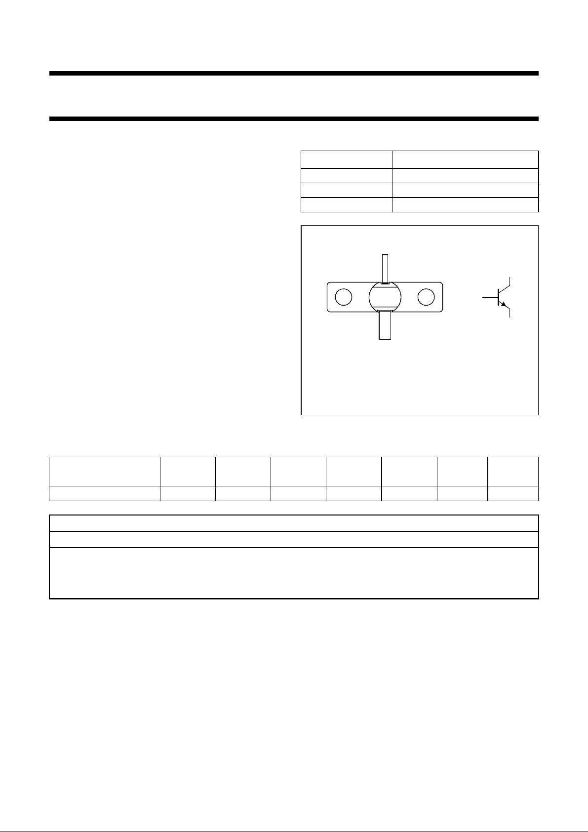
PINNING - SOT440A
PIN DESCRIPTION
1 collector
2 base
3 emitter connected to flange
olumns
Top view
Marking code: 502
Fig.1 Simplified outline and symbol.
1
c
b
3
2
MAM131
e
QUICK REFERENCE DATA
Microwave performance up to T
MODE OF OPERATION
=25°C in a common emitter class-A amplifier.
mb
f
(GHz)
V
(V)
CE
I
C
(mA)
P
L1
(mW)
G
po
(dB)
Z
(Ω)
i
Z
(Ω)
Class-A (CW) linear 4.2 18 110 ≥450 ≥6.6 100 + j40 4 + j4
WARNING
Product and environmental safety - toxic materials
This product contains beryllium oxide. The product is entirely safe provided that the BeO slab is not damaged.
All persons who handle, use or dispose of this product should be aware of its nature and of the necessary safety
precautions. After use, dispose of as chemical or special waste according to the regulations applying at the location of
the user. It must never be thrown out with the general or domestic waste.
L
1997 Feb 21 2
Page 3
Philips Semiconductors Product specification
NPN microwave power transistor LTE42005S
LIMITING VALUES
In accordance with the Absolute Maximum Rating System (IEC 134).
SYMBOL PARAMETER CONDITIONS MIN. MAX. UNIT
V
CBO
V
CER
V
CEO
V
EBO
I
C
P
tot
T
stg
T
j
T
sld
collector-base voltage open emitter − 40 V
collector-emitter voltage RBE= 100 Ω−35 V
collector-emitter voltage open base − 16 V
emitter-base voltage open collector − 3V
collector current (DC) − 250 mA
total power dissipation Tmb≤ 75 °C − 4W
storage temperature −65 +200 °C
operating junction temperature − 200 °C
soldering temperature at 0.3 mm from case; t = 10 s − 235 °C
3
10
handbook, halfpage
I
C
(mA)
(3)
2
10
10
(1) (2)
CEO
V
15 20 25 30 35
VCE (V)
10
1
Tmb≤ 75°C.
(1) Region of permissible DC operation.
(2) Permissible extension provided RBE≤ 100 Ω.
(3) Second breakdown limit (independent of temperature).
Fig.2 DC SOAR.
MBH902
handbook, halfpage
5
P
tot
(W)
4
3
2
1
0
−50 200
0 50 100 150
MGD966
Tmb (°C)
Fig.3 Power dissipation derating as a function of
mounting-base temperature.
1997 Feb 21 3
Page 4

Philips Semiconductors Product specification
NPN microwave power transistor LTE42005S
THERMAL CHARACTERISTICS
SYMBOL PARAMETER CONDITIONS MAX. UNIT
R
th j-mb
R
th mb-h
Note
1. See “
CHARACTERISTICS
=25°C unless otherwise specified
T
mb
SYMBOL PARAMETER CONDITIONS MIN. TYP. MAX. UNIT
I
CBO
I
CER
I
EBO
h
FE
C
cb
C
ce
C
eb
thermal resistance from junction to mounting-base Tj=75°C 36 K/W
thermal resistance from mounting-base to heatsink Tj=75°C; note 1 0.7 K/W
Mounting recommendations in the General part of handbook SC19a”
.
collector cut-off current VCB= 20 V; IE=0 −−0.1 µA
V
= 40 V; IE=0 −−0.25 mA
CB
emitter cut-off current VCE= 35 V; RBE= 100 Ω− − 1mA
emitter cut-off current VEB= 1.5 V; IC=0 −−0.2 µA
DC current gain VCE=5V; IC= 110 mA 15 − 150
collector-base capacitance VCB= 20 V; VEB= 1.5 V;
− 0.5 − pF
IE=IC= 0; f = 1 MHz
collector-emitter capacitance VCE= 20 V; VEB= 1.5 V;
− 1.5 − pF
IE=IC= 0; f = 1 MHz
emitter-base capacitance VCB= 10 V; VEB=1V;
− 6.5 − pF
IC=IE= 0; f = 1 MHz
1997 Feb 21 4
Page 5

Philips Semiconductors Product specification
NPN microwave power transistor LTE42005S
Table 1 Scattering parameters: VCE= 18 V; IC= 110 mA (VCE and IC regulated); Tmb=25°C; Zo=50Ω; typical
values. (The figures given between brackets are values in dB).
f
(MHz)
s
11
MAGNITUDE
(ratio)
ANGLE
(deg)
s
21
MAGNITUDE
(ratio)
ANGLE
(deg)
MAGNITUDE
(ratio)
s
12
ANGLE
MAGNITUDE
(deg)
(ratio)
s
22
ANGLE
(deg)
500 0.76 −176 0.022 (−33.2) 37 8.13 (18.2) 85 0.35 −62
600 0.75 180 0.023 (−32.8) 37 6.95 (16.8) 78 0.34 −66
700 0.76 177 0.023 (−32.8) 40 5.95 (15.5) 73 0.34 −71
800 0.76 174 0.024 (−32.5) 41 5.25 (14.4) 67 0.35 −75
900 0.76 171 0.024 (−32.3) 42 4.69 (13.4) 62 0.35 −79
1000 0.75 168 0.026 (−31.8) 43 4.23 (12.5) 57 0.36 −83
1100 0.75 165 0.028 (−31.0) 43 3.88 (11.8) 53 0.37 −87
1200 0.74 163 0.031 (−30.1) 43 3.61 (11.2) 49 0.39 −90
1300 0.75 160 0.035 (−29.2) 43 3.36 (10.5) 44 0.40 −95
1400 0.74 162 0.037 (−28.5) 44 3.12 (9.9) 41 0.43 −98
1500 0.73 157 0.041 (−27.8) 46 2.95 (9.4) 37 0.43 −101
1600 0.73 155 0.045 (−27.0) 46 2.83 (9.0) 32 0.45 −104
1700 0.71 154 0.047 (−26.5) 44 2.70 (8.6) 28 0.47 −107
1800 0.70 151 0.049 (−26.1) 43 2.56 (8.2) 23 0.48 −110
1900 0.69 148 0.050 (−25.9) 42 2.44 (7.7) 19 0.50 −114
2000 0.68 143 0.051 (−25.9) 39 2.34 (7.4) 14 0.51 −116
2200 0.67 138 0.058 (−24.7) 36 2.16 (6.7) 4 0.55 −124
2400 0.65 134 0.067 (−23.5 34 2.02(6.1) −2 0.59 −129
2600 0.62 129 0.077 (−22.3) 31 1.95 (5.8) −12 0.64 −134
2800 0.57 122 0.082 (−21.7) 25 1.84 (5.3) −21 0.68 −138
3000 0.52 113 0.086 (−21.3) 21 1.78 (5.0) −32 0.72 −143
3200 0.49 104 0.093 (−20.6) 16 1.67 (4.5) −42 0.74 −150
3400 0.45 99 0.102 (−19.8) 13 1.62 (4.2) −52 0.80 −157
3600 0.38 92 0.113 (−18.9) 8 1.52 (3.6) −64 0.80 −163
3800 0.29 83 0.119 (−18.5) 6 1.43 (3.1) −76 0.82 −170
4000 0.24 69 0.137 (−17.3) 2 1.27 (2.1) −88 0.80 −179
4200 0.20 54 0.165 (−15.7) −5 1.08 (0.7) −98 0.68 171
4400 0.15 28 0.202 (−13.9) −20 0.92 (0.8 −100 0.51 172
4600 0.12 −36 0.206 (−13.7) −38 0.93 (0.6) −102 0.52 −174
4800 0.17 −86 0.195 (−14.2) −52 0.97 (−0.3) −110 0.63 −171
5000 0.24 −114 0.177 (−15.0) −65 0.97 (−0.3) −122 0.73 −174
5200 0.31 −137 0.164 (−15.7 −73 0.93 (−0.6) −133 0.79 −180
5400 0.41 −152 0.154 (−16.2) −83 0.88 (−1.1) −145 0.83 174
5600 0.48 −161 0.134 (−17.4) −90 0.81 (−1.8) −156 0.85 166
5800 0.53 −168 0.122 (−18.2) −97 0.77 (−2.3) −167 0.87 160
6000 0.56 −179 0.105 (−19.6) −104 0.70 (−3.1) −178 0.89 154
1997 Feb 21 5
Page 6

Philips Semiconductors Product specification
NPN microwave power transistor LTE42005S
APPLICATION INFORMATION
Microwave performance up to T
=25°C in a common emitter class-A test circuit; note 1.
mb
MODE OF OPERATION
f
(GHz)
Class-A (CW) 4.2 18 110 ≥450 (26.5)
V
(V)
CE
(2)
I
(mA)
C
(2)
P
(mW)
L1
(3)
typ. 550 (27.4)
G
po
(4)
(dB)
≥6.6
typ. 7.2
Z
(Ω)
i
Z
(Ω)
100 + j40 4 + j4
Notes
1. Circuit consists of prematching circuit boards in combination with complementary input and output slug tuners.
and VCE regulated.
2. I
C
3. Load power for 1 dB compressed power gain.
4. Low level power gain associated with PL1.
4.5
10.4
5
10
30
15.5
1
output
VSWR <3
z0 = 50 Ω
MSA097
handbook, full pagewidth
input
VSWR <3
z0 = 50 Ω
0.8
4
2.8
11.5 13 5.5
30
3
2
L
Dimensions in mm.
Input striplines on a double copper-clad printed-circuit board with PTFE fibreglass dielectric (εr= 2.54); thickness: 1.6 mm.
Output striplines on a double copper-clad Rexolite printed-circuit board with dielectric (εr= 2.4); thickness: 0.25 mm.
Fig.4 Prematching test circuit board.
1997 Feb 21 6
Page 7

Philips Semiconductors Product specification
NPN microwave power transistor LTE42005S
600
handbook, halfpage
P
L
(mW)
400
200
0
0
f = 4.2 GHz; Tmb=25°C.
VCE= 18 V; IC= 110 mA (both regulated).
(1) Gpo= 7.2 dB.
50 100 150
(1)
typ
Pi (mW)
Fig.5 Load power as a function of input power.
MGL012
P
L1
1997 Feb 21 7
Page 8

Philips Semiconductors Product specification
NPN microwave power transistor LTE42005S
PACKAGE OUTLINE
ndbook, full pagewidth
3.45
2.90
3.2
2.9
0.1
seating plane
0.25
M
O
3
1.0
7.1
20.5 max
2.0
14.2
1
2
0.25 M
(1)3.4
MBC888
1.7 max
5.1
4.5
max
4.5
min
5.5
max
4.5
min
Dimensions in mm.
Torque on screw: Max. 0.4 Nm
Recommended screw: M2.5
Fig.6 SOT440A.
1997 Feb 21 8
Page 9

Philips Semiconductors Product specification
NPN microwave power transistor LTE42005S
DEFINITIONS
Data Sheet Status
Objective specification This data sheet contains target or goal specifications for product development.
Preliminary specification This data sheet contains preliminary data; supplementary data may be published later.
Product specification This data sheet contains final product specifications.
Limiting values
Limiting values given are in accordance with the Absolute Maximum Rating System (IEC 134). Stress above one or
more of the limiting values may cause permanent damage to the device. These are stress ratings only and operation
of the device at these or at any other conditions above those given in the Characteristics sections of the specification
is not implied. Exposure to limiting values for extended periods may affect device reliability.
Application information
Where application information is given, it is advisory and does not form part of the specification.
LIFE SUPPORT APPLICATIONS
These products are not designed for use in life support appliances, devices, or systems where malfunction of these
products can reasonably be expected to result in personal injury. Philips customers using or selling these products for
use in such applications do so at their own risk and agree to fully indemnify Philips for any damages resulting from such
improper use or sale.
1997 Feb 21 9
Page 10

Philips Semiconductors Product specification
NPN microwave power transistor LTE42005S
NOTES
1997 Feb 21 10
 Loading...