

Page 1
FEATURES
■
Guaranteed
■
Guaranteed
■
Typ Offset Drift: 0.01µV/°C
■
Excellent Long Term Stability: 100nV/√Month
■
Guaranteed
■
Over Operating Temperature Range:
Guaranteed
Guaranteed
Guaranteed
■
Single Supply Operation: 4.75V to 16V
Max Offset: 5µV
Max Offset Drift: 0.05µV/°C
Max Input Bias Current: 30pA
Min Gain: 120dB
Min CMRR: 120dB
Min PSRR: 120dB
(Input Voltage Range Extends to Ground)
■
External Capacitors can be Returned to V– with No
Noise Degradation
U
APPLICATIO S
■
Thermocouple Amplifiers
■
Strain Gauge Amplifiers
■
Low Level Signal Processing
■
Medical Instrumentation
LTC1052/LTC7652
Zero-Drift
Operational Amplifier
U
DESCRIPTIO
The LTC®1052 and LTC7652 are low noise zero-drift op
amps manufactured using Linear Technology’s enhanced
LTCMOSTM silicon gate process. Chopper-stabilization
constantly corrects offset voltage errors. Both initial offset
and changes in the offset due to time, temperature and
common mode voltage are corrected. This, coupled with
picoampere input currents, gives these amplifiers
unmatched performance.
Low frequency (1/f) noise is also improved by the
chopping technique. Instead of increasing continuously
at a 3dB/octave rate, the internal chopping causes noise to
decrease at low frequencies.
The chopper circuitry is entirely internal and completely
transparent to the user. Only two external capacitors
are required to alternately sample-and-hold the offset
correction voltage and the amplified input signal. Control
circuitry is brought out on the 14-pin and 16-pin versions
to allow the sampling of the LTC1052 to be synchronized
with an external frequency source.
, LTC and LT are registered trademarks of Linear Technology Corporation.
LTCMOS is a trademark of Linear Technology Corporation.
TYPICAL APPLICATIO
Ultralow Noise, Low Drift Amplifier Noise Spectrum
5V
INPUT
3
2
0.1µF
100k
V
OS = 3µV
V
OS∆T = 50nV/°C
NOISE = 0.06µV
+
LTC1052
–
1
5V
7
6
8
4
0.1µF
3K
0.1Hz TO 10Hz
P-P
–5V
3
2
0.1µF
1
+
LT®1007
–
U
–5V
160
140
120
100
80
VOLTAGE NOISE DENSITY (nV/√Hz)
60
40
20
0
0
FREQUENCY (Hz)
400100 200 300 500
LTC1052/7652 • TA02
1052fa
68k
5V
7
4
1.5k
8
6
5V
OUTPUT
100k
100Ω
LTC1052/7652 • TA01
1
Page 2
LTC1052/LTC7652
WWWU
ABSOLUTE AXI U RATI GS
(Notes 1 and 2)
Total Supply Voltage (V+ to V–) ............................... 18V
+
Input Voltage ........................ (V
+ 0.3V) to (V– – 0.3V)
Output Short Circuit Duration .......................... Indefinite
Storage Temperature Range .................. –55°C to 150°C
UU
W
PACKAGE/ORDER I FOR ATIO
TOP VIEW
C
EXTB
C
1
EXTA
2
–IN
3
+IN
METAL CAN H PACKAGE
OBSOLETE PACKAGE
ORDER PART NUMBER
8
–
+
4
–
V
+
V
/CASE
7
OUTPUT
6
5
LTC1052 OUTPUT CLAMP
LTC7652 C
RETURN
REPLACES
Operating Temperature Range
LTC1052C/LTC7652C ..........................–40°C to 85°C
LTC1052M (OBSOLETE).....................–55°C to 125°C
Lead Temperature (Soldering, 10 sec).................. 300°C
TOP VIEW
C
EXTB
C
EXTA
NC (GUARD)
–IN
+IN
NC (GUARD)
V–
1
2
3
4
–
5
+
6
7
N PACKAGE, 14-LEAD CERDIP
T
= 110°C, θJA = 130°C/W
JMAX
J PACKAGE, 14-LEAD CERDIP
INT/EXT
14
CLK IN
13
12
CLK OUT
V+
11
OUTPUT
10
OUTPUT CLAMP
9
C
RETURN
8
OBSOLETE PACKAGE
Consider the N14 Package for Alternate SourceConsider the N8 Package for Alternate Source
ORDER PART NUMBER
REPLACES
LTC7652CH
ICL7652CTV
ICL7652ITV
ICL7650CTV-1
ICL7650ITV-1
LTC1052CH
ICL7650CTV
ICL7650ITV
LTC1052MH
C
EXTA
–
IN
+N
–
V
T
J8 PACKAGE, 8-LEAD CERDIP
TOP VIEW
1
–
2
3
+
4
N8 PACKAGE
8-LEAD PDIP
= 110°C, θJA = 150°C/W
JMAX
ICL7650MTV
C
EXTB
8
+
V
7
6
OUTPUT
OUTPUT
5
CLAMP
OBSOLETE PACKAGE
Consider the N8 Package for Alternate Source
ORDER PART NUMBER
LTC1052CN8
LTC1052CJ8
LTC1052MJ8
Consult LTC Marketing for parts specified with wider operating temperature ranges.
REPLACES
ICL7650CPA
ICL7650IJA
ORDER PART NUMBER
LTC1052CN
LTC1052CJ
LTC1052MJ
C
1
EXTB
2
C
EXTA
NC (GUARD)
NC (GUARD)
3
4
–IN
5
+IN
6
7
V–
8
NC
16-LEAD PLASTIC (WIDE) SO
T
JMAX
LTC1052CSW
TOP VIEW
16
15
14
13
12
11
10
SW PACKAGE
= 110°C, θJA = 150°C/W
ICL7652CPD
ICL7650CPD
ICL7652IJD
ICL7650IJD
ICL7650MJD
INT/EXT
CLK IN
CLK OUT
V+
OUTPUT
OUTPUT CLAMP
C
RETURN
9
NC
REPLACES
LTC1052CS
1052fa
2
Page 3
LTC1052/LTC7652
ELECTRICAL CHARACTERISTICS
The ● denotes the specifications which apply over the full operating
temperature range, otherwise specifications are at TA = 25°C. VS = ±5V, test circuit TC1, unless otherwise noted.
LTC1052M LTC1052C/LTC7652C
SYMBOL PARAMETER CONDITIONS MIN TYP MAX MIN TYP MAX UNITS
V
OS
∆VOS/∆Temp Average Input Offset Drift (Note 3) ● ± 0.01 ±0.05 ±0.01 ±0.05 µV/°C
∆VOS/∆Time Long-Term Offset Voltage Stability 100 100 nV/√Month
I
OS
I
B
e
nP-P
I
n
CMRR Common Mode Rejection Ratio VCM = V– to 2.7V ● 120 140 120 140 dB
PSRR Power Supply Rejection Ratio V
A
VOL
V
OUT
SR Slew Rate RL = 10k, CL = 50pF 4 4 V/µs
GBW Gain Bandwidth Product 1.2 1.2 MHz
I
S
f
S
Note 1: Absolute Maximum Ratings are those values beyond which the life
of a device may be impaired.
Note 2: Connecting any terminal to voltages greater than V
–
, may cause destructive latch-up. It is recommended that no sources
V
operating from external supplies be applied prior to power-up of the
LTC1052/LTC7652.
Note 3: These parameters are guaranteed by design. Thermocouple effects
preclude measurement of the voltage levels in high speed automatic
Input Offset Voltage (Note 3) ±0.5 ± 5 ±0.5 ± 5 µV
Input Offset Current ±30 ±90 ±30 ±90 pA
● ±2000 ±350 pA
Input Bias Current ±1 ±30 ±1 ±30 pA
● ±1000 ±175 pA
Input Noise Voltage RS = 100Ω, DC to 10HZ, TC3 1.5 1.5 µV
RS = 100Ω, DC to 1HZ, TC3 0.5 0.5 µV
P-P
P-P
Input Noise Current f = 10Hz (Note 5) 0.6 0.6 fA/√Hz
= ±2.375V to ±8V ● 120 150 120 150 dB
SUPPLY
Large-Signal Voltage Gain RL = 10k, V
= ±4V ● 120 150 120 150 dB
OUT
Maximum Output Voltage Swing RL = 10k ● ±4.7 ±4.85 ±4.7 ±4.85 V
(Note 4) R
= 100k ±4.95 ±4.95 V
L
Supply Current No Load 1.7 2.0 1.7 2.0 mA
● 3.0 3.0 mA
Internal Sampling Frequency 330 330 Hz
Clamp On Current RL = 100k ● 25 100 25 100 µA
Clamp Off Current –4V < V
< 4V 10 100 10 100 pA
OUT
+
, or less than
● 21nA
testing. V
capability. Voltages on C
is measured to a limit determined by test equipment
OS
EXTA
and C
EXTB
, A
, CMRR and PSRR are
VOL
measured to insure proper operation of the nulling loop to ensure meeting
the V
and V
OS
drift specifications. See Package-Induced VOS in the
OS
Applications Information section.
Note 4: Output clamp not connected.
Note 5: Current noise is calculated from the formula: i
q = 1.6 • 10
–19
coulomb.
n
= (2q IB)
1/2
, where
UW
TYPICAL PERFOR A CE CHARACTERISTICS
Input Noise Voltage
5µV
0
5µV
0
10 SEC.
VS = ±5V, TEST CIRCUIT (TC3)
DC TO 1Hz
DC TO 10Hz
1052fa
3
Page 4
LTC1052/LTC7652
UW
TYPICAL PERFOR A CE CHARACTERISTICS
Offset Voltage vs Sampling
Frequency
12
V
SUPPLY= ±5V
10
8
(µV)
6
OS
V
4
2
0
0
500 1000 1500 2000
SAMPLING FREQUENCY, fS (Hz)
Aliasing Error
VS = ±5V
AV = –1
TEST CIRCUIT TC2
(3Hz BANDWIDTH)
OUTPUT SPECTRUM (dB)
fI–f
S
50Hz/DIV
LTC1052/7652 • TPC01
f
S
1OHz
Frequency
5
4
3
2
1
10Hz PEAK-TO-PEAK NOISE (µV)
0
100
Common Mode Input Range vs
Supply Voltage
8
6
4
2
0
–2
–4
COMMON MODE RANGE (V)
f
I
–6
–8
0
Noise vs Sampling
P-P
V
SUPPLY= ± 5V
SAMPLING FREQUENCY, fS (Hz)
1
2
1k 10k
4
3
SUPPLY VOLTAGE (±V)
VCM = V
5
LTC1052/7652 • TPC02
–
6
7
Input Bias Current vs
Temperature
1000
900
800
(pA)
B
700
600
500
400
300
200
INPUT BIAS CURRENT, I
100
0
–50
0
–25
AMBIENT TEMPERATURE, TA(°C)
GUARANTEED
25
50
GUARANTEED
75
100
LTC1052/7652 • TPC03
125
Overload Recovery
(Output Clamp Not Used)
VS = ±5V
IV/DIV
OVERDRIVE
REMOVED
AV = –100
8
50ms/DIV
LTC1052/7652 • TPC04
Small-Signal Transient Response* Gain Phase vs Frequency
OUTPUT VOLTAGE (20mV/DIV)
AV = 1
RL = 10k
CL = 100pF
VS = ±5V
*RESPONSE IS NOT DEPENDENT ON PHASE OF CLOCK
2µs/DIV
Large-Signal Transient Response*
OUTPUT VOLTAGE (2mV/DIV)
AV = 1
RL = 10k
CL = 100pF
VS = ±5V
2µs/DIV
120
100
80
60
40
20
VOLTAGE GAIN (dB)
0
–20
–40
100 10
3
10
GAIN
4
FREQUENCY (Hz)
4
10
PHASE
5
VS= ±5V
= 100pF
C
L
6
10
LTC1052/LTC7652 • TPC06
60
80
PHASE SHIFT (DEGREES)
100
120
140
160
180
200
220
7
10
1052fa
Page 5
UW
0.1µF
0.1µF
1k
V
REF
*
3
2
7
6
8
4
1
–5V
1k
5V
+
–
LTC1052
LTC1052/7652 • TPC13
V
IN
* – 5V ≤ V
REF
≤ 2.7V
5
TYPICAL PERFOR A CE CHARACTERISTICS
LTC1052/LTC7652
Broadband Noise, C
(5µV/DIV)
INPUT REFERRED NOISE
AV = –1000 1ms/DIV
EXT
= 0.1µF
Supply Current vs Supply Voltage
2.5
2.0
(mA)
S
1.5
1.0
SUPPLY CURRENT, I
0.5
0
6581012
4
TOTAL SUPPLY VOLTAGE, V+ TO V– (V)
LTC1052/LTC7652 • TPC08
14 16
Broadband Noise, C
(5µV/DIV)
INPUT REFERRED NOISE
AV = –1000 1ms/DIV
3.0
SUPPLY VOLTAGE = ± 5V
(mA)
S
2.0
1.0
SUPPLY CURRENT, I
0
–50
–25 0
AMBIENT TEMPERATURE, TA (°C)
= 1.0µF Broadband Noise Test Circuit (TC2)
EXT
50 100 125
25 75
LTC1052/LTC7652 • TPC09
R2
1M
R1
1k
R3
1k
C
EXTA
2
3
5V
–
LTC1052
+
1
–5V
Output Short-Circuit Current vs
Supply VoltageSupply Current vs Temperature
8
6
OUT (mA)
4
2
0
–10
–20
SHORT-CIRCUIT OUTPUT CURRENT, I
–30
5
4
68
TOTAL SUPPLY VOLTAGE, V+ TO V– (V)
I
SOURCE VOUT
I
SINK VOUT
10 14
7
6
8
4
C
EXTB
LTC1052/7652 • TPC07
–
= V
+
= V
12 16
LTC1052/LTC7652 • TPC10
Sampling Frequency vs Voltage Comparator Operation
600
500
(Hz)
S
400
300
200
SAMPLING FREQUENCY, f
100
0
4
TA = 25°C
5
681012
TOTAL SUPPLY VOLTAGE, V+ TO V– (V)
LTC1052/LTC7652 • TPC11
14 16
Sampling Frequency vs
Temperature
600
SUPPLY VOLTAGE = ± 5V
500
(Hz)
S
400
300
200
SAMPLING FREQUENCY, f
100
0
–50
–25 0
AMBIENT TEMPERATURE, TA (°C)
50 100 125
25 75
LT1052/LTC7652 • TPC12
1052fa
5
Page 6
LTC1052/LTC7652
UW
TYPICAL PERFOR A CE CHARACTERISTICS
Response Time vs Overdrive
V
+ OVERDRIVE
REF
INPUT
{
OUTPUT
– 1mV
V
REF
10µV
5µV
20ms/DIV
{
–5V
5V
50µV
TEST CIRCUITS
Electrical Characteristics Test Circuit (TC1) DC to 10Hz and DC to 1HZ Noise Test Circuit (TC3)
C2
R2
1M
R1
0.1µF
2
3
10Hz
1Hz
R2
–
LTC1052
+
1
V
V
+
7
4
–
16.2Ω
16.2Ω
2
3
–
LTC1052
+
1
+
V
7
6
8
4
0.1µF
–
V
OUTPUT
R
L
LTC1052/7652 • TC01
BANDWIDTH
R1
1k
0.1µF
C3
R4
R3
6
8
0.1µF
R1
R2
162k
162k
R3
16.2k
162k
3
+
C4
LT1001
2
–
34k
R4
16.2k
162k
34k
C2
0.1µF
1.0µF
6
OUTPUT
(NOISE x 20,000)
C3
1.0µF
1.0µF
C4
1.0µF
1.0µF
LTC1052/7652 • TC02
U
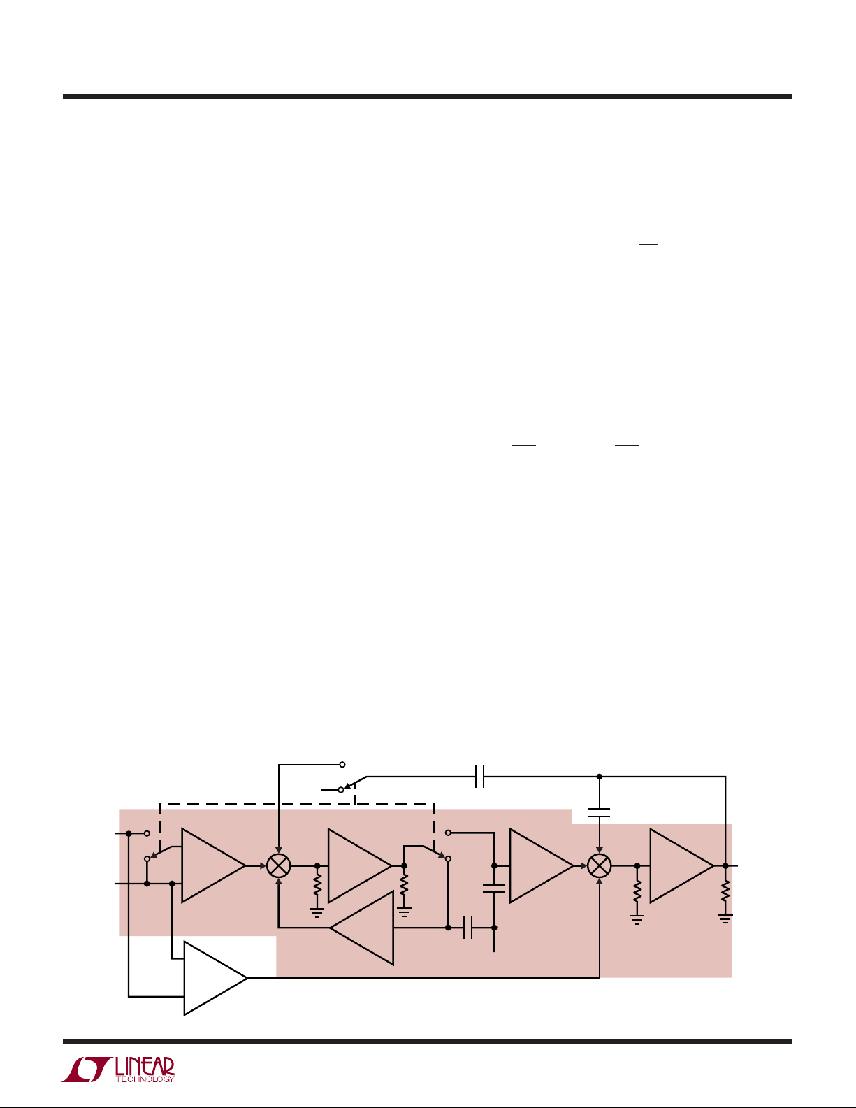
THEORY OF OPERATIO
DC OPERATION
The shaded portion of the LTC1052 block diagram
(Figure 1a) entirely determines the amplifier’s DC
characteristics. During the auto zero portion of the cycle,
the g
inputs are shorted together and a feedback path is
m1
closed around the input stage to null its offset. Switch S2
and capacitor C
act as a sample-and-hold to store the
EXTA
nulling voltage during the next step—the sampling cycle.
In the sampling cycle, the zeroed amplifier is used to
amplify the differential input voltage. Switch S2 connects
the amplified input voltage to C
and the output gain
EXTB
6
stage. C
and S2 act as a sample-and-hold to store the
EXTB
amplified input signal during the auto zero cycle.
By switching between these two states at a frequency
much higher than the signal frequency, a continuous
output results.
Notice that during the auto zero cycle the g
inputs are
m1
not only shorted together, but are also shorted to the
inverting input. This forces nulling with the common mode
voltage present and accounts for the extremely high
CMRR of the LTC1052. In the same fashion, variations in
1052fa
Page 7
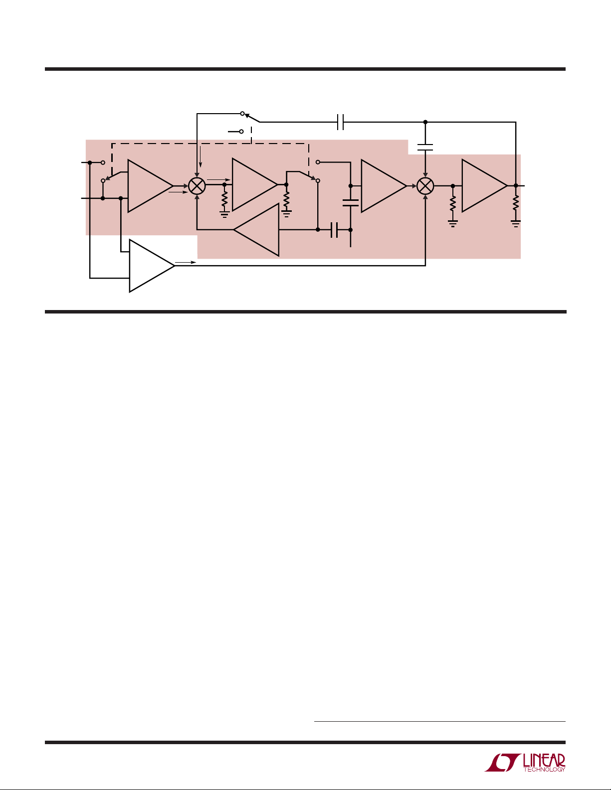
THEORY OF OPERATIO
LTC1052/LTC7652
U
power supply are also nulled. For nulling to take place, the
offset voltage, common mode voltage and power supply
must not change at a frequency which is high compared to
the frequency response of the nulling loop.
AC OPERATION AND ALIASING ERRORS
So far, the DC performance of the LTC1052 has been
explained. As the input signal frequency increases, the
problem of aliasing must be addressed. Aliasing is the
spurious formation of low and high frequency signals
caused by the mixing of the input signal with the sampling
frequency, fS. The frequency of the error signals, fE, is:
fE = fS ±f
I
where fI = input signal frequency.
Normally it is the difference frequency (fS – fI ) which is of
concern because the high frequency (fS + fI) can be easily
filtered. As the input frequency approaches the sampling
frequency, the difference frequency approaches zero and
will cause DC errors—the exact problem that the zero-drift
amplifier is meant to eliminate.
The solution is simple; filter the input so the sampling loop
never sees any frequency near the sampling frequency.
At a frequency well below the sampling frequency, the
LTC1052 forces I1 to equal I2 (see Figure 1b). This makes
δ l zero, thus the gain of the sampling loop zero at this and
higher frequencies (i.e., a low pass filter). The corner
frequency of this low pass filter is set by the output stage
pole (1/RL4 gm5 RL5 C2).
S3
V
REF
+IN
–IN
S1
+
g
m1
–
–
+
–
R
L1
g
m2
R
L2
V
g
m3
NULL
For frequencies above this pole, I2 is:
I2 = VIN gm6 •
1
• SC1
SC2
and
I1 – I2 = VIN gm1 – VIN gm6 •
The LTC1052 is very carefully designed so that gm1 = g
C1
C2
m6
and C1 = C2. Substituting these values in the above equation shows I1 – I2 = 0.
The gm6 input stage, with Cl and C2, not only filters the
input to the sampling loop, but also acts as a high
frequency path to give the LTC1052 good high frequency
response. The unity-gain cross frequencies for both the
DC path and high frequency path are identical
[f3dB =
1
(gm1/C1) =
2π
1
(gm6/C2)]
2π
thereby making the frequency response smooth and continuous while eliminating sampling noise in the output as
the loop transitions from the high gain DC loop to the high
frequency loop.
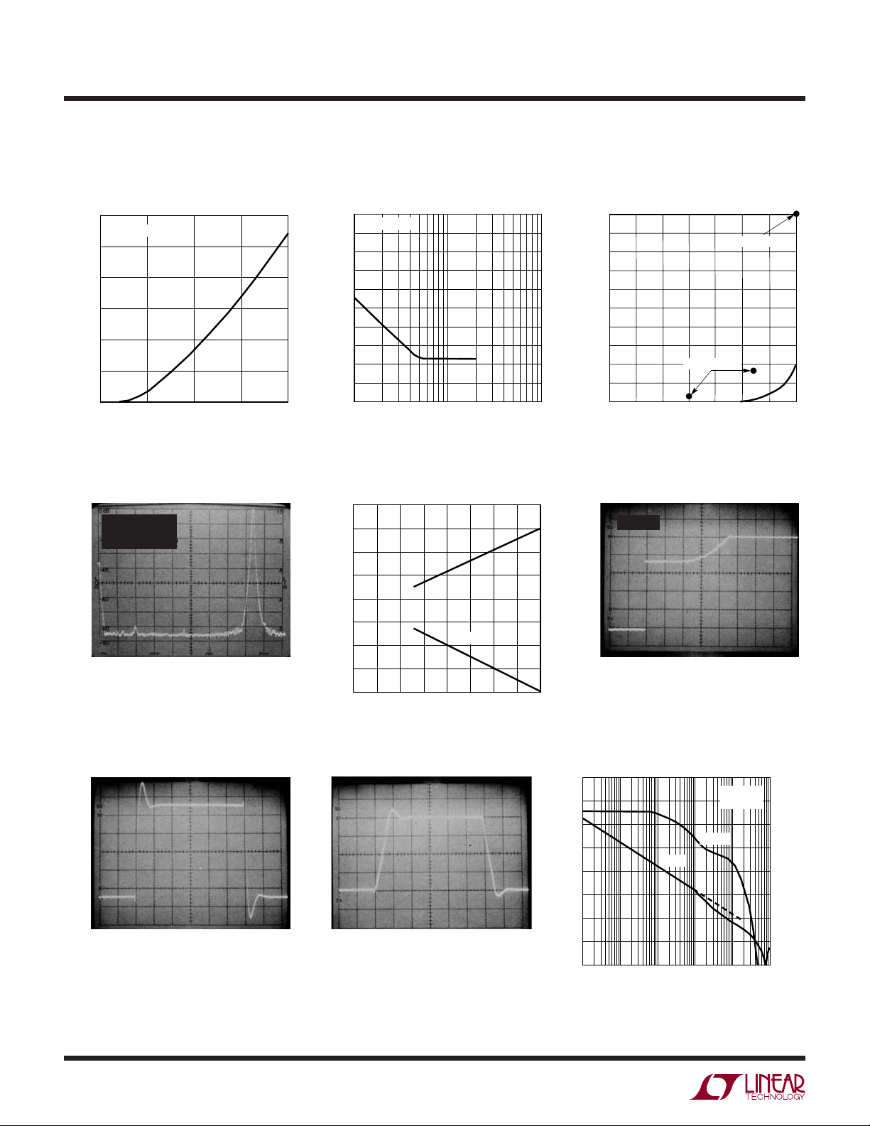
The typical curves show just how well the amplifier works.
The output spectrum shows that the difference frequency
(fI–fS = 100Hz) is down by 80dB and the frequency
response curve shows no abnormalities or perturbations.
Also note the well-behaved small and large-signal step
responses and the absence of the sampling frequency in
the output spectrum. If the dynamics of the amplifier
(i.e., slew rate and overshoot), depend on the sampling
clock, the sampling frequency will appear in the output
spectrum.
C1
C2
S2
g
m4
C
EXT B
C
EXT A
–
+
+
R
L4
g
m5
V
OUT
R
L5
–
g
m6
+
Figure 1a. LTC1052 Block Diagram
Auto Zero Cycle
V–
LTC1052/7652 • TPC13
1052fa
7
Page 8
LTC1052/LTC7652
U
THEORY OF OPERATIO
S3
V
REF
l
+IN
–IN
S1
+
g
m1
–
–
g
m6
+
2
δl
–
+
–
l
1
R
L1
l
3
Figure 1b. LTC1052 Block Diagram
WUUU
APPLICATIO S I FOR ATIO
g
m2
g
m3
Sampling Cycle
C1
C2
S2
g
m4
R
L2
C
EXT B
C
EXT A
–
V
–
+
+
R
L4
g
m5
LTC1052/7652 • TO02
V
OUT
R
L5
EXTERNAL CAPACITORS
C
EXTA
and C
are the holding elements of a sample-
EXTB
and-hold circuit. The important capacitor characteristics
are leakage current and dielectric absorption. A high
quality film-type capacitor such as mylar or polypropylene
provides excellent performance. However, low grade
capacitors such as ceramic are suitable in many
applications.
Capacitors with very high dielectric absorption (ceramic)
can take several seconds to settle after power is first
turned on. This settling appears as clock ripple on the
output and, as the capacitor settles, the ripple gradually
disappears. If fast settling after power turn-on is
important, mylar or polypropylene is recommended.
Above 85°C, leakage, both from the holding capacitors
and the printed circuit board, becomes important. To
maintain the capabilities of the LTC1052 it may be
necessary to use PTFE capacitors and PTFE standoffs
when operating at 125°C (see Achieving Picoampere/
Microvolt Performance).
C
EXTA
and C
are normally in the range of 0.1µF
EXTB
to 1.0µF. All specifications are guaranteed with 0.1µF and
the broadband noise (refer to Typical Performance Characteristics) is only very slightly degraded with 0.1µF.
Output clock ripple is not present for capacitors of 0.1µF
or greater at any temperature.
On competitive devices, connecting C
EXTA
and C
EXTB
to
V– causes an increase in amplifier noise. Design changes
have eliminated this problem on the LTC1052. On the
14-pin LTC1052 and 8-pin LTC7652, the capacitors can
be returned to V– or C
RETURN
with no change in noise
performance.
ACHIEVING PICOAMPERE/MICROVOLT PERFORMANCE
Picoamperes
In order to realize the picoampere level of accuracy of the
LTC1052, proper care must be exercised. Leakage
currents in circuitry external to the amplifier can
significantly degrade performance. High quality insulation
should be used (e.g., PTFE, Kel-F); cleaning of all
insulating surfaces to remove fluxes and other residues
will probably be necessary—particularly for high
temperature performance. Surface coating may be
necessary to provide a moisture barrier in high humidity
environments.
Board leakage can be minimized by encircling the input
connections with a guard ring operated at a potential
close to that of the inputs: in inverting configurations, the
guard ring should be tied to ground; in noninverting
1052fa
8
Page 9

WUUU
APPLICATIO S I FOR ATIO
LTC1052/LTC7652
connections, to the inverting input. Guarding both sides
of the printed circuit board is required. Bulk leakage
reduction depends on the guard ring width.
Microvolts
Thermocouple effects must be considered if the LTC1052’s
ultralow drift is to be fully utilized. Any connection
of dissimilar metals forms a thermoelectric junction
producing an electric potential which varies with
temperature (Seebeck effect). As temperature sensors,
thermocouples exploit this phenomenon to produce
useful information. In low drift amplifier circuits the effect
is a primary source of error.
Figure 2 is an example of the introduction of an
unnecessary resistor to promote differential thermal
balance. Maintaining compensating junctions in close
physical proximity will keep them at the same temperature
and reduce thermal EMF errors.
NOMINALLY UNNECESSARY
RESISTOR USED TO
THERMALLY BALANCE OTHER
INPUT RESISTOR
RESISTOR LEAD, SOLDER,
COPPER TRACE JUNCTION
Figure 2
LEAD WIRE/SOLDER/COPPER
TRACE JUNCTION
+
LTC1052
–
OUTPUT
LTC1052/7652 • AI03
When connectors, switches, relays and/or sockets are
necessary they should be selected for low thermal EMF
activity. The same techniques of thermally balancing and
coupling the matching junctions are effective in reducing
the thermal EMF errors of these components.
Connectors, switches, relay contacts, sockets, resistors,
solder, and even copper wire are all candidates for
thermal EMF generation. Junctions of copper wire from
different manufacturers can generate thermal EMFs of
200nV/°C—4 times the maximum drift specification of
the LTC1052. The copper/kovar junction, formed when
wire or printed circuit traces contact a package lead, has
a thermal EMF of approximately 35µV/°C–700 times the
maximum drift specification of the LTC1052.
Minimizing thermal EMF-induced errors is possible if
judicious attention is given to circuit board layout and
component selection. It is good practice to minimize the
number of junctions in the amplifier’s input signal path.
Avoid connectors, sockets, switches and relays where
possible. In instances where this is not possible, attempt
to balance the number and type of junctions so that
differential cancellation occurs. Doing this may involve
deliberately introducing junctions to offset unavoidable
junctions.
Resistors are another source of thermal EMF errors.
Table 1 shows the thermal EMF generated for different
resistors. The temperature gradient across the resistor is
important, not the ambient temperature. There are two
junctions formed at each end of the resistor and if these
junctions are at the same temperature, their thermal EMFs
will cancel each other. The thermal EMF numbers are
approximate and vary with resistor value. High values give
higher thermal EMF.
Table 1. Resistor Thermal EMF
RESISTOR TYPE THERMAL EMF/°C GRADIENT
Tin Oxide ~mV/’C
Carbon Composition ~450µV/°C
Metal Film ~20µV/°C
Wire Wound
Evenohm ~2µV/°C
Manganin ~2µV/°C
1052fa
9
Page 10

LTC1052/LTC7652
WUUU
APPLICATIO S I FOR ATIO
When all of these errors are considered, it may seem
impossible to take advantage of the extremely low drift
specifications of the LTC1052. To show that this is not the
case, examine the temperature test circuit of Figure 3. The
lead lengths of the resistors connected to the amplifier’s
inputs are identical. The thermal capacity and thermal
resistance each input sees is balanced because of the
symmetrical connection of resistors and their identical
size. Thermal EMF-induced shifts are equal in phase and
amplitude, thus cancellation occurs.
50k
–
LTC1052
+
5V
7
6
8
4
V
• 1000
1
OS
0.1µF
LTC1052/7652 • AI04
2
0.1µF
100Ω
50k
3
0.1µF
–5V
Figure 3. Offset Drift Test Circuit
Figure 4 shows the response of this circuit under
temperature transient conditions. Metal film resistors and
an 8-pin DIP socket were used. Care was taken in the
construction to thermally balance the inputs to the
amplifier. The units were placed in an oven and allowed to
stabilize at 25°C. The recording was started and after
100 seconds the oven, preset to 125°C, was switched on.
The test was first performed on an 8-pin plastic package
and then was repeated for a TO-5 package plugged into the
same test board. It is significant that the change in VOS,
even under these severe thermal transient conditions,
is quite good. As temperature stabilizes, note that the
steady-state change of VOS is well within the maximum
±0.05µV/°C drift specification.
Very slight air currents can still affect even this
arrangement. Figure 5 shows strip charts of output noise
both with the circuit covered and with no cover in “still” air.
This data illustrates why it is often prudent to enclose the
LTC1052 and its attendant components inside some form
of thermal baffle.
0 MIN 25 MIN20 MIN5 MIN
10
25°C TO 125°C
0
(10µV/DIV)
OS
10
OFFSET VOLTAGE, V
0
OVEN SWITCHED
ON (25°C)
PLASTIC
25°C TO 125°C
METAL CAN
OVEN STABILIZED
AT 12 MIN
100 SECONDS/IN
±0.05µV/°C
±0.05µV/°C
Figure 4. Transient Response of Offset Drift Test Circuit with 100°C Temperature Step
10
1052fa
Page 11

WUUU
APPLICATIO S I FOR ATIO
#1 COVERED
1µV
Figure 5. DC to 1Hz (Test Circuit TC3)
LTC1052/LTC7652
#1 UNCOVERED
#2 UNCOVERED
20 SEC
PACKAGE-INDUCED OFFSET VOLTAGE
Since the LTC1052 is constantly fixing its own offset, it
may be asked why there is any error at all, even under
transient temperature conditions. The answer is simple.
The LTC1052 can only fix offsets inside its own nulling
loop. There are many thermal junctions outside this loop
that cannot be distinguished from legitimate signals.
Some have been discussed previously, but the package
thermal EMF effects are an important source of errors.
Notice the difference in the thermal response curves of
Figure 4. This can only be attributed to the package since
everything else is identical. In fact, the VOS specification is
set by the package-induced warm-up drift, not by the
LTC1052. TO-99 metal cans exhibit the worst warm-up
drift and Linear Technology sample tests TO-99 lots to
minimize this problem.
Two things make 100% screening costly: (1) The extreme
precision required on the LTC1052 and (2) the thermal
time constant of the package is 0.5 to 3 minutes, depending on package type. The first precludes the use of automatic handling equipment and the second takes a long
time. Bench test equipment is available to 100% test for
warmed-up drift if offsets of less than ±5µV are required.
CLOCK
The LTC1052 has an internal clock, setting the nominal
sampling frequency at 330Hz. On 8-pin devices, there is
no way to control the clock externally. In some applications it may be desirable to control the sampling clock and
this is the function of the 14-pin device.
CLK IN, CLK OUT and INT/EXT are provided to accomplish
this. With no external connection, an internal pull-up holds
INT/EXT at the V+ supply and the 14-pin device selfoscillates at 330Hz. In this mode there is a signal on the
CLK IN pin of 660Hz (2 times sampling frequency) with a
30% duty cycle. A divide-by-two drives the CLK OUT pin
and sets the sampling frequency.
To use an external clock, connect INT/EXT to V– and the
external clock to CLK IN. The logic threshold of CLK IN is
2.5V below the positive supply; this allows CMOS logic to
drive it directly with logic supplies of V+ and ground. CLK
IN can be driven from V+ to V– if desired. The duty cycle of
the external clock is not particularly critical but should be
kept between 30% and 60%.
Capacitance between CLK IN and CLK OUT (pins 13 and
12) can cause the divide-by-two circuit to malfunction. To
avoid this, keep this capacitance below 5pF.
1052fa
11
Page 12

LTC1052/LTC7652
WUUU
APPLICATIO S I FOR ATIO
OUTPUT CLAMP
If the LTC1052 is driven into saturation, the nulling loop,
attempting to force the differential input voltage to zero,
will drive C
EXTA
and C
to a supply rail. After the
EXTB
saturating drive is removed, the capacitors take a finite
time to recover—this is the overload recovery time. The
overload recovery is longest when the capacitors are
driven to the negative rail (refer to Overload Recovery in
the Typical Performance Characteristics section). The
overload recovery time in this case is typically 225ms. In
the opposite direction (i.e., C
EXTA
and C
at positive
EXTB
rail), it is about ten times faster (25ms). The overload
recovery time for the LTC1052 is much faster than competitive devices; however, if a faster overload recovery
time is necessary, the output clamp function can be used.
When the output clamp is connected to the negative input
it prevents the amplifier from saturating, thus keeping
C
EXTA
and C
at their nominal voltages. The output
EXTB
clamp is a switch that turns on when the output gets to
within approximately 1V of either supply rail. This switch
is in parallel with the amplifier’s feedback resistor. As the
output moves closer to the rail, the switch on
resistance decreases, reducing the closed loop gain. The
output swing is reduced when the clamp function is used.
How much current the output clamp leaks when off
is important because, when used, it is connected to the
amplifier’s negative input. Any current acts like input bias
current and will degrade accuracy. At the other extreme,
the maximum current the clamp conducts when on determines how much overdrive the clamp will take, and still
keep the amplifier from saturating. Both of these numbers
are guaranteed in the Electrical Characteristics section.
LOW SUPPLY OPERATION
The minimum supply voltage for proper operation of the
LTC1052 is typically 4.0V (±2.0V). In single supply
applications, PSRR is guaranteed down to 4.7V (±2.35V).
This assures proper operation down to the minimum TTL
specified voltage of 4.75V.
U
TYPICAL APPLICATIO S
5V Powered Ultraprecision Instrumentation Amplifier Fast Precision Inverter
+IN
–IN
5V
4
11
12
LTC1043
2
3
0.0047µF
8
C1
C3
1µF
C2
1µF1µF
R1
14
5
15
16
100
+
C4
1µF
CIRCUITRY WITHIN DASHED LINES MAY BE DELETED IF OUTPUT
DOES NOT HAVE TO SWING ALL THE WAY TO GROUND
DRIFT = 50nV/°C
V
= 3µV
OS
R2
GAIN =
+ 1
R1
CMRR = >120dB DC – 20kHz
BANDWIDTH =10Hz
7
13
5V
43k
1N914
6
18
17
3
2
0.1µF
≈ – 0.5V
R2
100k
+
LTC1052
–
4
5V
1
0.22µF
10k*
7
6
8
0.1µF
10k
V
OUT
LTC1052/7652 • TA03
INPUT
10k
0.1µF
10k
1N4148
300pF
5V
2
7
+
LTC1052
3
8
–
4
1
–5V
*1% METAL FILM
FULL POWER BANDWIDTH = 2MHz
SLEW RATE = 40V/µs
SETTLING (10V STEP) = 12µs TO 0.01%
BIAS CURRENT DC = 30pA
OFFSET DRIFT = 50nV/°C
OFFSET VOLTAGE = 5µV
6
0.1µF
10k
1000pF
2
+
3
–
10k*
8pF
5V
LT318A
–5V
7
6
OUTPUT
4
LTC1052/7652 • TA04
1052fa
12
Page 13

TYPICAL APPLICATIO S
+
COMPARATOR
INPUTS
GROUND OR
INPUT COMMON-
MODE VOLTAGE
–
U
14 13
8
LTC1043
5
Offset Stabilized Comparator
5V
4
12
11
7
1M
6
2
3
0.1µF
2
3
2
3
+
LTC1052
–
1
1µF
5V
+
–
–5V
7
4
5V
8
LT1011
4
8
1
6
0.1µF
LTC1052/LTC7652
150Ω330Ω
2k
6
7
5
10k
COMPARATOR
OUTPUT (± 5V)
5V
ZERO COMMAND
5V =ZERO
–5V=COMPARE
1HZ to 1.25MHz Voltage-to-Frequency Converter (5V Supply)
5V
3
7
+
LTC1052
2
–
0.1µF 0.1µF
FULL-SCALE TRIM
30.1k*
V
IN
OV TO 5V
TRW MTR–5/ +1200ppm/°C
*
POLYSTYRENE–WESCO #32–P/ – 120ppm/°C
**
±0.05%
>120dB
0.01Hz/°C
20ppm/°C
LINEARITY
DYNAMIC RANGE
ZERO POINT DRIFT
GAIN DRIFT
4
1
10k
(1.25MHz)
6
8
0.22µF
15 18
16
17
–5V
3.3k
0.01µF
2k
8
14 13
10k
470Ω
330pF
1/2
470Ω
Q1
2N2907
5V
4
11
100pF**
12
LTC1043
17
–5V
0.01µF
5V
10k
7
LT1004-1.2V
16
74C04
5V
3.3pF
10k
0.1µF
STATUS OUTPUT
OV = ZERO
5V = COMPARE
LTC1052/7652 • TA05
LTC1052/7652 • TA06
NC
2N3904
OUTPUT
1H to 1.25MHz
1052fa
13
Page 14

LTC1052/LTC7652
TYPICAL APPLICATIO S
No VOS Adjust* CMOS DAC Buffer—Single Supply Air Flow Detector
15V
R
FB
12–BIT CMOS DAC
43k
6 5
1N914
15
1pF
16
l
OUT2
l
OUT1
1/2
15V
4
11
+
12
LTC1043
17
C
0.1µF
*
F
1k
15
5
2
+
LTC1052
3
–
1
0.1µF
1µF
NON POLARIZED
≈ – 0.5V
15V
4
U
7
8
LTC1052/7652 • TA07
6
0.1µF
V
OUT
FOR HIGHER SPEED, REFER TO
“FAST PRECISION INVERTER”
UNDER TYPICAL APPLICATIONS
10k
*OFFSET VOLTAGE CAUSES
NONLINEARITY ERRORS.
SEE: “APPLICATION GUIDE
TO CMOS MULTIPLYING D/A
CONVERTERS,”
ANALOG DEVICES, INC.
100k
± 1%
LT1004-1.2
43.2Ω
± 1%
AMBIENT
TEMPERATURE
STILL AIR
10k
1k
0.1µF
–
+
3
2
+
LTC1052
–
1
5V
5
7
6
5V = NO AIR FLOW
0V = AIR FLOW
8
4
0.1µF
–
TYPE K
LTC1052/7652 • TA08
+
AIR FLOW
240Ω
OV TO 3V
1Hz TRIM
IN
STABILIZING
AMP
3
2
0.1µF
16.2k*
5V
10k
–5V
+
LTC1052
–
100k
100k
1
2k
30MHz
TRIM
1000M
–5V
1Hz to 30MHz Voltage-to-Frequency Converter
5V
120Ω
CURRENT
7
6
8
4
0.1µF
0.0.1µF
10k
0.22µF
CHARGE
8
†
100pF
14
1/2
SOURCE
7.5k
PUMP
11
12
LTC1043
12k
2N3906
7
0.22µF
10
13
16
120Ω
100pF
5V
11
0.1µF
2k
LT1004–1.2V
5V
5
7490
10
1
1
12
FET BUFFER
2N5486
50Ω
2N5486
50Ω
–5V
14
5
5V
74S741/2
74S132
14
7
5V
TRIGGER
HP5082-2810
3
NC
RESET DIODE
2N3904
*TRW MTR-5/ + 120ppm/°C
†WESCO #32-P/ – 120ppm/°C
0.3Hz/°C ZERO-DRIFT
±0.08% LINEARITY
20ppm/°C GAIN DRIFT
150dB DYNAMIC RANGE
1Hz TO 30MHz
OUTPUT
LTC1052/7652 • TA09
OUT
14
1052fa
Page 15

100k
LOAD
5k
2.5k
1k
220Ω
6
7
2
8
4
2000pF
1
3
5V
100Ω
LTC1052/7652 • TA11
OUTPUT
INPUT
10k
+
–
LTC1052
OUTPUT SWING
± 4.92V
± 4.84V
± 4.65V
± 3.65V
5V
220pF
74C04
10k
0.1µF 0.1µF
TYPICAL APPLICATIO S
±100mA Output Drive Increasing Output Current
100k
V
IN
0.1µF
5V
2
7
3
–
LTC1052
+
1
6
8
4
0.1µF
–5V
VOS=5µV
/∆T=50µV/°C
V
OS
GAIN =10
FULL POWER BANDWIDTH =1kHz
100pF
LTC1010
Single 5V Thermocouple Amplifier with Cold Junction Compensation
U
–5V
LTC1052/LTC7652
5V
1M
V
OUT
±100mA
R
L
LTC1052/7652 • TA10
5V
100k
LT1004-1.2
1690Ω
187Ω
43k
5V
R1
1820Ω
IN914
0.0047µF
5k AT 25°C
7
13
6
18
16
5V
†
11
12
+
LTC1043
17
+
V
T
–
4
8
1µF
14
5
2
1µF
3
15
1k
5V
3
7
–
LTC1052
2
+
1
1µF
1µF
†
*CHOOSE C
0.1µF
NONPOLARIZED
≈– 0.5V
YELLOW SPRINGS INST. CO. PART #44007
10k
TO FILTER NOISE
F
8
4
LTC1052/7652 • TA12
6
0.1µF
R
F
R
V
OUT
CF*
l
THERMOCOUPLE
TYPE
J
K
T
S
R
F
= VT1+
()
R
l
R1
232k
301k
301k
2.1M
1052fa
15
Page 16

LTC1052/LTC7652
TYPICAL APPLICATIO S
U
Increasing Output Current and Voltage (V
7V
2N3904
INPUT
3k
STABLE FOR ALL GAINS, INVERTING
AND NONINVERTING, OBSERVE
LTC1052 COMMON MODE INPUT LIMITS
2
3
–
LTC1052
+
1
–7V
0.1µF
7
4
0.1µF
NC
3
6
8
0.1µF0.1µF
2N3904
NC
+
LT318A
2
–
Precision Multiplexed Differential Thermocouple Amplifier
COLD JUNCTION
COMPENSATOR
LT1004–1.2V
1690Ω
187Ω
100k
R1
1820Ω
5k AT
25°C
†
SUPPLY
15V
30k 33pF
7
6
4
–15V
= ±15V) DC Stabilized FET Probe
INPUT CAPACITANCE BOOTSTRAP
5V
FAST SOURCE
FOLLOWER
OUTPUT
±12V AT 20mA | LIMIT
3k
1k
LTC1052/7652 • TA13
4
7
11
12
1µF
INPUT
0.1µF
3
0.1µF
2
–
LTC1052
+
8
1µF
10M
Q2
2N2222
100Ω
–5V
DC STABILIZATION
5V
7
4
1
–5V
Q1
2N5486
1N4148
DRAIN CURRENT SINK
10k
0.01µF
2000pF
1k
6
8
0.1µF
1M
LT1010
–5V
V
OUT
0.1µF
5V
0.1µF
6
8
BANDWIDTH: 20MHz
†
DELAY: 5ns
= 1001 • V
+
V
7
+
LTC1052
–
4
1
: 100ns
RISE
THERMOCOUPLE
OUTPUT
10M
3
0.1µF
2
0.1µF
LTC1052/7652 • TA14
16
5V
16
12
1
14
5
15
2
11
4
78
–5V
13
3
9
10
CD4052B
13
6
18
LTC1043
16
0.0047µF
–5V
ADDRESS
14
TYPE
K
T
S
1k
J
R1
232k
301k
301k
2.1M
LTC1052/7652 • TA15
1052fa
5
2
1µF
3
15
17
1µF
†
YELLOW SPRINGS INST. CO. PART #44007
THERMOCOUPLE
Page 17

TYPICAL APPLICATIO S
–
+
FILTER-AND-OVERLOAD
TYPE K
THERMOCOUPLE 41.4µV/°C
CLAMP
50k
60°C TRIM
A
187Ω*
†
1N914
COLD JUNCTION BIAS
100k
1µF
OPTIONAL INPUT
STABILIZING AMP
150k**
33k**
1µF
487Ω*
3
2
0.1µF
301k*
U
Direct Thermocouple-to-Frequency Converter
R
+
LTC1052
–
1
5
100pF
5V
7
4
–5V
3300pF
LTC1043
T
1.8k*
33k
6
8
0.1µF
16
6
0.1µF
2
COLD JUNCTION TEMPERATURE TRACKING
1N4148
A
74C04
0.68µF
5V
74C04
F
–5V
4.75k*
1k*
LT1004–1.2V
LTC1052/LTC7652
470Ω
C10k B
820pF
5V
3k
0.01% FILM-TRW MAR-6
*
TRW/MTR/5/ + 120
**
= YELLOW SPRINGS INST. #44007
R
T
100pF = POLYSTYRENE
†
FOR GENERAL PURPOSE (1mV FULL-SCALE)
10-BIT A-TO-D, REMOVE THERMOCOUPLE—
COLD JUNCTION NETWORK, GROUND POINT A,
AND DRIVE LTC1052 POSITIVE INPUT
E
D
5V
74C903
OUTPUT
0Hz TO 600Hz
0°C TO 60°C
LTC1052/7652 • TA16
3
2
1000pF
1
+
LM301A
–
5V
8
4
7
–5V
BRIDGE DRIVE
Direct 10-Bit Strain Gauge Digitizer
5V
5V
20Ω
STRAIN GAUGE
1N4148
1N4148
TRANSDUCER
= 350Ω
Z
IN
= 350Ω
Z
OUT
7
3.3M
13
22.3k*
470k*
1/2 LTC1043
SW1
SW2
20Ω
1k
6
2N2905
–5V
28k
1000pF
3.3MΩ*
11
16
12
14
–5V
INTEGRATOR
2
–
LTC1052
3
+
0.01µF
8
1k*
74C00
14k
CLOCK
5V
7
6
8
4
1
0.01µF
–5V
CONNECT DIRECTLY
ACROSS BRIDGE
DRIVE POINTS
+
33µF
2
0.003µF
5V
1/2 74C74
7
–5V
4114
10k
5V
10k
3
5
6
*0.1% METAL FILM TRW MAR-5
100k
1/2 74C903
5V
–5V
OUTPUT
GATING
OUT A
DATA OUTPUT =
SW1 =MAIN CURRENT SWITCH
SW2 =CURRENT LOADING COMPENSATION SWITCH
CONNECT TO BRIDGE
END OF 470k RESISTOR
TRANSDUCER ZERO NETWORK
= 1000 COUNTS FULL-SCALE
OUT B
(OPTIONAL)
LTC1052/7652 • TA17
FREQUENCY
OUT B
FREQUENCY
OUT A
1052fa
17
Page 18

LTC1052/LTC7652
TYPICAL APPLICATIO S
U
16-Bit A/D Converter
74C00
E
OV TO 5V
IN
10k
FULL-SCALE
TRIM
95k*
0.1µF
2
3
28k
0.01µF
–
LTC 1052
+
1
2N4338
5V
4
–5V
7
A2
8
INTEGRATOR
75k*
14k
CLOCK
6
2
1/2
0.1µF
5V
7
6
LTC1052
8
4
–5V
CURRENT SINK
5V
24114
74C74
5
76
3
+
2
–
1
0.1µF0.1µF
820pF
10pF
1k
LT1009
5V
B
OUT
10k
1/3
74C903
5V
A
OUT
–5V
5V
16
13
1µF39pF
20k
–5V
0.01µF
LINEARITY
TRIM
7
18
4
14
12
11
8
15
18
A
DATA OUTPUT =
100,000 COUNTS FULL-SCALE
NO ZERO TRIM
20ppm/°C GAIN DRIFT
*VISHAY S-102 RESISTOR
OUT
B
OUT
CURRENT SWITCH
3
LTC1043
17
–5V
LTC1052/7652 • TA18
1052fa
Page 19

TYPICAL APPLICATIO S
LTC1052/LTC7652
U
Precision Isolation Amplifier
INPUT
FLOATING
SUPPLY
OUTPUTS
100k
– 15V
25mA
15V
25mA
NC
4
–
5
+
11
NC
2N3904
+
2.2µF
FLOATING COMMON
LTC1052
14–PIN
13
10
2
7
1
14
11
74C90 74C90
2N3904
2.2µF
+
0.1µF0.1µF
55
14
11
1
1N4148
100k*
1010
1k*
10k
2N5434
14
÷10÷10
2k
1212
1
2k
1N4148 1N4148
11k
DALE TC–10–11
4.3k
10k
L1
4
5
7
8
OUTPUT SIDEINPUT SIDE
1
2N5434
2
L2
STANCOR PCT-39
2N54342N5434
36
15V
1.8k
1
2N2222
POWER
DRIVER
15V
2
2N2222
39
10k
68pF
1k
74C04
10k
100pF
68pF
– 15V
1000pF
74C04
330Ω
ZERO TRIM
100k
74C04
1000pF
20k
20k
22M
15V
3
2
IN4148
10M
(SELECT)
1
+
LTC1052
–
15V
– 15V
30pF
7
– 15V
20k
4
8
6
1k GAIN TRIM
13.3k*
10k*
OUT
250V ISOLATION
0.03% ACCURACY
*1% FILM RESISTOR
1.8k
15V
1k
LTC1052/7652 • TA19
1052fa
19
Page 20

LTC1052/LTC7652
PACKAGE DESCRIPTIO
SEATING
PLANE
(0.254 – 1.143)
45°TYP
U
H Package
8-Lead TO-5 Metal Can (.200 Inch PCD)
(Reference LTC DWG # 05-08-1320)
.335 – .370
(8.509 – 9.398)
DIA
.305 – .335
(7.747 – 8.509)
.016 – .021**
(0.406 – 0.533)
PIN 1
.010 – .045*
.028 – .034
(0.711 – 0.864)
.040
(1.016)
MAX
.050
(1.270)
MAX
.027 – .045
(0.686 – 1.143)
GAUGE
PLANE
.200
(5.080)
TYP
.165 – .185
(4.191 – 4.699)
.500 – .750
(12.700 – 19.050)
REFERENCE
PLANE
.110 – .160
(2.794 – 4.064)
INSULATING
STANDOFF
*
LEAD DIAMETER IS UNCONTROLLED BETWEEN THE REFERENCE PLANE
AND THE SEATING PLANE
**
FOR SOLDER DIP LEAD FINISH, LEAD DIAMETER IS
.016 – .024
(0.406 – 0.610)
OBSOLETE PACKAGE
H8(TO-5) 0.200 PCD 0801
20
1052fa
Page 21

PACKAGE DESCRIPTIO
U
J Package
14-Lead CERDIP (Narrow .300 Inch, Hermetic)
(Reference LTC DWG # 05-08-1110)
.785
12
(19.939)
MAX
11 891013
.005
(0.127)
MIN
14
LTC1052/LTC7652
.025
(0.635)
RAD TYP
.300 BSC
(7.62 BSC)
.008 – .018
(0.203 – 0.457)
NOTE: LEAD DIMENSIONS APPLY TO SOLDER DIP/PLATE
OR TIN PLATE LEADS
0° – 15°
1
.045 – .065
(1.143 – 1.651)
OBSOLETE PACKAGE
234
.014 – .026
(0.360 – 0.660)
56
7
.100
(2.54)
BSC
.220 – .310
(5.588 – 7.874)
.200
(5.080)
MAX
.015 – .060
(0.381 – 1.524)
.125
(3.175)
MIN
J14 0801
1052fa
21
Page 22

LTC1052/LTC7652
PACKAGE DESCRIPTIO
U
J8 Package
8-Lead CERDIP (Narrow .300 Inch, Hermetic)
(Reference LTC DWG # 05-08-1110)
CORNER LEADS OPTION
(4 PLCS)
.023 – .045
(0.584 – 1.143)
HALF LEAD
.045 – .068
(1.143 – 1.650)
FULL LEAD
OPTION
.300 BSC
(7.62 BSC)
.008 – .018
(0.203 – 0.457)
NOTE: LEAD DIMENSIONS APPLY TO SOLDER DIP/PLATE
OR TIN PLATE LEADS
OPTION
0° – 15°
OBSOLETE PACKAGE
8-Lead PDIP (Narrow .300 Inch)
(Reference LTC DWG # 05-08-1510)
.005
(0.127)
MIN
.025
(0.635)
RAD TYP
.045 – .065
(1.143 – 1.651)
.014 – .026
(0.360 – 0.660)
N8 Package
.405
(10.287)
MAX
87
12
65
3
4
.220 – .310
(5.588 – 7.874)
.015 – .060
(0.381 – 1.524)
.100
(2.54)
BSC
.200
(5.080)
MAX
.125
3.175
MIN
J8 0801
22
87 6
.255 ± .015*
(6.477 ± 0.381)
1234
.300 – .325
(7.620 – 8.255)
.065
(1.651)
.008 – .015
(0.203 – 0.381)
+.035
.325
–.015
+0.889
8.255
()
–0.381
NOTE:
1. DIMENSIONS ARE
*THESE DIMENSIONS DO NOT INCLUDE MOLD FLASH OR PROTRUSIONS.
MOLD FLASH OR PROTRUSIONS SHALL NOT EXCEED .010 INCH (0.254mm)
INCHES
MILLIMETERS
TYP
.045 – .065
(1.143 – 1.651)
.100
(2.54)
BSC
.400*
(10.160)
MAX
5
.130 ± .005
(3.302 ± 0.127)
.120
(3.048)
MIN
.018 ± .003
(0.457 ± 0.076)
.020
(0.508)
MIN
N8 1002
1052fa
Page 23

PACKAGE DESCRIPTIO
U
N Package
14-Lead PDIP (Narrow .300 Inch)
(Reference LTC DWG # 05-08-1510)
14
.255 ± .015*
(6.477 ± 0.381)
1213
.770*
(19.558)
MAX
11
LTC1052/LTC7652
8910
.300 – .325
(7.620 – 8.255)
.008 – .015
(0.203 – 0.381)
+.035
.325
–.015
+0.889
8.255
()
–0.381
NOTE:
1. DIMENSIONS ARE
*THESE DIMENSIONS DO NOT INCLUDE MOLD FLASH OR PROTRUSIONS.
MOLD FLASH OR PROTRUSIONS SHALL NOT EXCEED .010 INCH (0.254mm)
INCHES
MILLIMETERS
.020
(0.508)
MIN
.130 ± .005
(3.302 ± 0.127)
.120
(3.048)
MIN
.005
(0.125)
MIN
2
31
.045 – .065
(1.143 – 1.651)
.100
(2.54)
BSC
6
7
.065
(1.651)
TYP
.018 ± .003
(0.457 ± 0.076)
N14 1002
5
4
Information furnished by Linear Technology Corporation is believed to be accurate and reliable.
However, no responsibility is assumed for its use. Linear Technology Corporation makes no representation that the interconnection of its circuits as described herein will not infringe on existing patent rights.
1052fa
23
Page 24

LTC1052/LTC7652
PACKAGE DESCRIPTIO
.030 ±.005
TYP
N
U
SW Package
16-Lead Plastic Small Outline (Wide .300 Inch)
(Reference LTC DWG # 05-08-1620)
.050 BSC
.045 ±.005
16
N
.398 – .413
(10.109 – 10.490)
15 14
NOTE 4
13
12
10 9
11
.420
MIN
123 N/2
RECOMMENDED SOLDER PAD LAYOUT
.291 – .299
(7.391 – 7.595)
NOTE 4
.010 – .029
.005
(0.127)
RAD MIN
.009 – .013
(0.229 – 0.330)
NOTE:
1. DIMENSIONS IN
2. DRAWING NOT TO SCALE
3. PIN 1 IDENT, NOTCH ON TOP AND CAVITIES ON THE BOTTOM OF PACKAGES ARE THE MANUFACTURING OPTIONS.
THE PART MAY BE SUPPLIED WITH OR WITHOUT ANY OF THE OPTIONS
4. THESE DIMENSIONS DO NOT INCLUDE MOLD FLASH OR PROTRUSIONS.
MOLD FLASH OR PROTRUSIONS SHALL NOT EXCEED .006" (0.15mm)
(0.254 – 0.737)
NOTE 3
INCHES
(MILLIMETERS)
× 45°
.016 – .050
(0.406 – 1.270)
.325 ±.005
0° – 8° TYP
NOTE 3
.093 – .104
(2.362 – 2.642)
(1.270)
1
.050
BSC
(0.356 – 0.482)
2345
.014 – .019
TYP
6
.394 – .419
(10.007 – 10.643)
N/2
78
.037 – .045
(0.940 – 1.143)
.004 – .012
(0.102 – 0.305)
S16 (WIDE) 0502
24
Linear Technology Corporation
1630 McCarthy Blvd., Milpitas, CA 95035-7417
(408) 432-1900 ● FAX: (408) 434-0507
●
www.linear.com
1052fa
LW/TP 1202 1K REV A • PRINTED IN USA
LINEAR TECHNOLOGY CORPORATION 1985
 Loading...