

Page 1
LTC6412
800MHz, 31dB Range
Analog-Controlled VGA
FEATURES
n
800MHz –3dB Small-Signal Bandwidth
n
Continuously-Adjustable Gain Control
n
–14dB to +17dB Linear-in-dB Gain Range
n
35dBm OIP3 at 240MHz Across All Gain Settings
n
10dB Noise Figure at Maximum Gain
n
(IIP3 – NF) = +8dBm at 240MHz Across All Gains
n
2.7nV/√Hz Input Referred Noise
n
Differential Inputs and Outputs
n
50Ω Input Impedance Across all Gains
n
Single Supply Operation from 3V to 3.6V
n
110mA Supply Current
n
4mm × 4mm × 0.75mm 24-Pin QFN Package
APPLICATIONS
n
IF Signal Chain Automatic Gain Control (AGC)
n
2.5G and 3G Cellular Basestation Transceivers
n
WiMAX, WiBro, WLAN Receivers
n
Satellite and GPS Receiver IF
DESCRIPTION
The LTC®6412 is a fully differential variable gain amplifi er
with linear-in-dB analog gain control. It is designed for
AC-coupled operation in IF receiver chains from 1MHz
to 500MHz. The part has a constant OIP3 across a wide
output amplitude range and across the 31dB gain control
range. The output noise (NF + Gain) is also fl at versus gain
to provide a uniform spurious-free dynamic range (SFDR)
>120dB over the full gain control range at 240MHz.
®
The LTC6412 is ideal for interfacing with the LT
LT5557 downconverting mixers, LTC6410-6 IF amplifi er
and the LTC6400/LTC6401/LTC6416 ADC drivers for use
in 12-, 14-, and 16-bit ADC applications.
The LTC6412 recovers quickly from an overdrive condition,
and the EN pin allows for a fast output signal disable to
protect sensitive downstream components. Asserting the
SHDN pin reduces the current consumption below 1mA
for power-down or sleep modes.
L, LT, LTC, LTM, Linear Technology and the Linear logo are registered trademarks of Linear
Technology Corporation. All other trademarks are the property of their respective owners.
5527 and
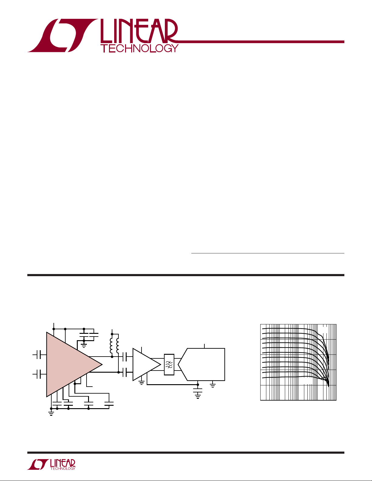
TYPICAL APPLICATION
3.3V Fully Differential 240MHz IF Receiver Chain with 31dB Gain Control
3.3V
3.3V
+OUT
G
+V
REF
V
–OUT
0.1μF
GAIN CONTROL
(+ SLOPE MODE)
0.1μF
0.1μF
180nH180nH
10nF
IF INPUT
10nF
10nF
+IN
–IN
V
GND
CC
LTC6412
CM
V
SHDN
DECL2
DECL1
1nF
–V
0.1μF
EN
G
0.1μF
0.1μF
3.3V
+
+IN
V
LTC6400-8
V
CM
–
–IN
V
+OUT
–OUT
BPF
VGA Gain vs Frequency
Over Gain Control Range
20
3.3V
V
DD
+
A
IN
LTC2208
–
A
IN
V
GND
CM
6412 TA01
2.2μF
10
0
GAIN (dB)
–10
–20
–30
1 100 1000 10000
10
FREQUENCY (MHz)
G
MAX
G
MIN
6412 G01
6412fa
1
Page 2
LTC6412
(Note 1)
Total Supply Voltage (VCC to GND) ...........................3.8V
Amplifi er Input Current (+IN, –IN) ........................±20mA
Amplifi er Output Current (+OUT, –OUT) ...............±70mA
Input Current (+V
Input Current (V
, –VG, V
G
, DECL1, DECL2) ....................±10mA
CM
RF Input Power, Continuous, 50Ω ......................+15dBm
RF Input Power, 100μs pulse, 50Ω ....................+20dBm
Operating Temperature Range (Note 2).... –40°C to 85°C
Specifi ed Temperature Range (Note 3) .... –40°C to 85°C
Storage Temperature Range ...................–65°C to 150°C
Junction Temperature ........................................... 150°C
, EN, SHDN ) .........±10mA
REF
PIN CONFIGURATION ABSOLUTE MAXIMUM RATINGS
TOP VIEW
VCCGND
SHDNENGND
24 23 22 21 20 19
1
+IN
2
–IN
3
V
4
CM
V
5
CM
6
V
CC
24-LEAD (4mm s 4mm) PLASTIC QFN
T
EXPOSED PAD (PIN 25) IS GND, MUST BE SOLDERED TO PCB
JMAX
25
7 8 9
DECL1
10 11 12
G
+V
GND
UF PACKAGE
= 150°C, θJA = 37°C/W
CC
V
GND
18GND
+OUT
17
–OUT
16
GND
15
DECL2
14
13
V
CC
G
REF
–V
GND
V
ORDER INFORMATION
LEAD FREE FINISH TAPE AND REEL PART MARKING* PACKAGE DESCRIPTION SPECIFIED TEMPERATURE RANGE
LTC6412CUF#PBF LTC6412CUF#TRPBF 6412
LTC6412IUF#PBF LTC6412IUF#TRPBF 6412
24-Lead (4mm × 4mm) Plastic QFN
24-Lead (4mm × 4mm) Plastic QFN
Consult LTC Marketing for parts specifi ed with wider operating temperature ranges. *The temperature grade is identifi ed by a label on the shipping container.
Consult LTC Marketing for information on non-standard lead based fi nish parts.
For more information on lead free part marking, go to: http://www.linear.com/leadfree/
For more information on tape and reel specifi
cations, go to: http://www.linear.com/tapeandreel/
0°C to 70°C
–40°C to 85°C
2
6412fa
Page 3
LTC6412
DC ELECTRICAL CHARACTERISTICS
The l denotes specifi cations that apply over the full operating
temperature range, otherwise specifi cations are at T
V
is defi ned as (+IN) – (–IN). V
IN(DIFF)
OUT(DIFF)
is defi ned as (+OUT) – (–OUT). V
defi ned as [(+OUT) + (–OUT)]/2. Unless noted otherwise, default operating conditions are V
to V
(negative gain slope mode), V
REF
= 3.3V. Differential power gain defi ned at Z
OUT(CM)
differential.
SYMBOL PARAMETER CONDITIONS MIN TYP MAX UNITS
Gain Characteristics
G
MAX
G
MIN
G
RANGE
TC
GAIN
G
SLOPE
G
CONF(AVE)
G
CONF(MAX)
+IN and –IN Pins
R
IN(GMAX)
R
IN(GMIN)
V
INCM(GMAX)
V
INCM(GMIN)
, –VG, and V
+V
G
R
IH(+VG)
R
IH(–VG)
I
IL(+VG)
I
IL(–VG)
V
REF
Maximum Differential Power Gain (Note 4) –VG = 0V, V
Minimum Differential Power Gain (Note 4) –VG = 1.2V, V
Differential Power Gain Range G
Temperature Coeffi cient of Gain at Fixed V
Gain Control Slope –VG = 0.2V to 1.0V, 85 Points, Slope of the
Average Conformance Error to Gain Slope Line –VG = 0.2V to 1.0V, 85 Points, Standard
Maximum Conformance Error to Gain Slope
Line
Differential Input Resistance at Maximum Gain –VG = 0V, V
Differential Input Resistance at Minimum Gain –VG = 1.2V, V
Input Common Mode Voltage at Maximum Gain –VG = 0V, DC Blocking Capacitor to Input 640 mV
Input Common Mode Voltage at Minimum Gain –VG = 1.2V, DC Blocking Capacitor to Input 640 mV
Pins
REF
+VG Input High Resistance +VG = 1.0V, –VG Tied to V
–VG Input High Resistance –VG = 1.0V, +VG Tied to V
+VG Input Low Current +VG = 0V, –VG Tied to V
–VG Input Low Current –VG = 0V, +VG Tied to V
Internal Bias Voltage –VG = 0V, +VG Tied to V
= 25°C. DC electrical performance measured using DC test circuit schematic.
A
= 100mV
IN(DIFF)
= 200mV
IN(DIFF)
MAX-GMIN
–VG = 0V to 1.2V –0.007 dB/°C
G
Least-Square Fit Line
is defi ned as [(+IN) + (–IN)]/2. V
IN(CM)
= 3.3V, EN = 0.8V, SHDN = 2.2V, +VG tied
CC
= 50Ω differential and Z
SOURCE
16.1
l
15.5
–16.2
l
–16.8
30.7
l
30.1
–34.1
l
–34.7
OUT(CM)
LOAD
17.1 18.1
18.7
–14.9 –13.6
–13.0
31.9 33.1
33.7
–32.9 –31.7
–31.1
is
= 200Ω
0.12 0.20 dB
Error to the Least-Square Fit Line
–VG = 0.2V to 1.0V, 85 points, Maximum
0.20 0.45 dB
Error to the Least-Square Fit Line
R
IN(+VG)
R
IN(–VG)
IN(DIFF)
IN(DIFF)
= 1V/Δ I
= 1V/Δ I
= 100mV
= 200mV
IL(+VG)
IL(–VG)
REF
REF
REF
REF
REF
,
,
49
l
47
49
l
47
7.8
l
7.2
7.8
l
7.2
–9
l
–10
–9
l
–10
590
l
580
57 65
67
57 65
67
9.2 10.6
11.6
9.2 10.6
11.6
–5 –1
–1
–5 –1
–1
615 640
650
dB
dB
dB
dB
dB
dB
dB/V
dB/V
kΩ
kΩ
kΩ
kΩ
μA
μA
μA
μA
mV
mV
Ω
Ω
Ω
Ω
6412fa
3
Page 4
LTC6412
DC ELECTRICAL CHARACTERISTICS
The l denotes specifi cations that apply over the full operating
temperature range, otherwise specifi cations are at T
V
is defi ned as (+IN) – (–IN). V
IN(DIFF)
OUT(DIFF)
is defi ned as (+OUT) – (–OUT). V
defi ned as [(+OUT) + (–OUT)]/2. Unless noted otherwise, default operating conditions are V
to V
(negative gain slope mode), V
REF
= 3.3V. Differential power gain defi ned at Z
OUT(CM)
differential.
SYMBOL PARAMETER CONDITIONS MIN TYP MAX UNITS
SHDN Pin
V
IL(SHDN)
V
IH(SHDN)
I
IL(SHDN)
I
IH(SHDN)
EN Pin
V
IL(EN)
V
IH(EN)
I
IL(EN)
I
IH(EN)
Power Supply
V
S
I
S(TOT)
I
S(OUT)
I
Δ(OUT)
I
S(SHDN)
PSRR
MAX
PSRR
MIN
SHDN Input Low Voltage
SHDN Input High Voltage
SHDN Input Low Current SHDN = 0.8V
SHDN Input High Current SHDN = 2.2V
EN Input Low Voltage
EN Input High Voltage
EN Input Low Current EN = 0.8V
EN Input High Current EN = 2.2V
Operating Supply Range
Total Supply Current All VCC Pins Plus +OUT and –OUT Pins
Sum of Supply Current to OUT Pins I
Delta of Supply Current to OUT Pins Current Imbalance to +OUT and –OUT
Supply Current in Shutdown I
Power Supply Rejection Ratio at Max Gain –VG = 0V, Output Referred 40 53 dB
Power Supply Rejection Ratio at Min Gain –VG = 1.2V, Output Referred 40 53 dB
= 25°C. DC electrical performance measured using DC test circuit schematic.
A
is defi ned as [(+IN) + (–IN)]/2. V
IN(CM)
= 3.3V, EN = 0.8V, SHDN = 2.2V, +VG tied
CC
= 50Ω differential and Z
SOURCE
l
l
2.2 V
l
–60 –30 –1 μA
l
–30 –15 –1 μA
l
l
2.2 V
l
–60 –30 –1 μA
l
–30 –15 –1 μA
l
3.0 3.3 3.6 V
is
OUT(CM)
= 200Ω
LOAD
0.8 V
0.8 V
110 135
S(OUT)
= I
+OUT
+ I
–OUT
l
44 55
l
140
60
0.5 1.5
at SHDN = 0.8V
S(OUT)
l
0.5 1.3
l
2.0
2.0
mA
mA
mA
mA
mA
mA
mA
mA
4
6412fa
Page 5
LTC6412
AC ELECTRICAL CHARACTERISTICS
The l denotes specifi cations that apply over the full operating
temperature range, otherwise specifi cations are at T
(Figure 3, Test Circuit A) unless otherwise noted. Default operating conditions are VCC = 3.3V, EN = 0.8V, SHDN = 2.2V, +VG tied to V
(negative gain slope mode), and Z
SYMBOL PARAMETER CONDITIONS MIN TYP MAX UNITS
Small Signal
BW
GMAX
BW
GMIN
Sdd11 Input Match at Z
Sdd22 Output Match at Z
Sdd12 Reverse Isolation –VG = 0V to 1.2V, 10MHz-500MHz,
Transient Response
t
STEP(6dB)
t
STEP(12dB)
t
STEP(20dB)
t
OVDR
t
OFF
t
ON
70MHz Signal
G
MAX
G
MIN
G
RANGE
HD2 Second Harmonic Distortion P
HD3 Third Harmonic Distortion P
IM3 Third-Order Intermodulation f
OIP3 Output Third-Order Intercept f
P1dB
NF
GMAX
NF
GMIN
140MHz Signal
G
MAX
G
MIN
G
RANGE
HD2 Second Harmonic Distortion P
HD3 Third Harmonic Distortion P
–3dB Bandwidth for Sdd21 at Maximum Gain –VG = 0V, Test Circuit B 800 MHz
–3dB Bandwidth for Sdd21 at Minimum Gain –VG = 1.2V, Test Circuit B 800 MHz
= 50Ω Differential –VG = 0V to 1.2V, 10MHz-500MHz,
SOURCE
= 200Ω Differential –VG = 0V to 1.2V, 10MHz-250MHz,
LOAD
6dB Gain Step Response Time Peak P
12dB Gain Step Response Time Peak P
20dB Gain Step Response Time Peak P
Overdrive Recovery Time at 70MHz –VG = 0V, PIN = +3dBm to –17dBm, Time to
Output Amplifi er Disable Time P
Output Amplifi er Enable Time P
Maximum Gain –VG = 0V, Test Circuit B 17 dB
Minimum Gain –VG = 1.2V, Test Circuit B –15 dB
Gain Range G
Output 1dB Compression Point at Max Gain –VG = 0V (Note 6) 13 dBm
GMAX
Noise Figure at Maximum Gain –VG = 0V (Note 5) 10 dB
Noise Figure at Minimum Gain –VG = 1.2V (Note 5) 42 dB
Maximum Gain –VG = 0V, Test Circuit B 17 dB
Minimum Gain –VG = 1.2V, Test Circuit B –15 dB
Gain Range G
SOURCE
= Z
LOAD
= 25°C. Typical AC electrical performance measured in demo board DC1464A
A
= 50Ω unless otherwise noted.
Test Circuit B
Test Circuit B
Test Circuit B
= +4dBm, –VG = 0.2V to 0.4V,
OUT
Time to Settle Within 1dB of Final P
= +4dBm, –VG = 0.2V to 0.6V,
OUT
Time to Settle Within 1dB of Final P
= +4dBm, –VG = 0.2V to 0.8V,
OUT
Time to Settle Within 1dB of Final P
Settle Within 1dB of Final P
= 0dBm at EN = 0V, –VG = 0V,
OUT
EN = 0V to 3V, Time for P
= 0dBm at EN = 0V, –VG = 0V, EN = 3V to
OUT
0V, Time for P
MAX-GMIN
OUT
OUT
= 69.5MHz, f2 = 70.5MHz,
1
P
OUT
= 69.5MHz, f2 = 70.5MHz,
1
P
OUT
MAX-GMIN
OUT
OUT
OUT
= 0dBm, –VG = 0V to 1.0V –80 dBc
= 0dBm, –VG = 0V to 1.0V –80 dBc
= –6dBm/Tone, –VG = 0V to 1.0V
= –6dBm/Tone, –VG = 0V to 1.0V
= 0dBm, –VG = 0V to 1.0V –80 dBc
= 0dBm, –VG = 0V to 1.0V –75 dBc
OUT
≥ –1dBm
OUT
OUT
OUT
OUT
≤ –20dBm
–20 dB
–10 dB
-80 dB
0.4 μs
0.4 μs
0.4 μs
25 ns
25 ns
20 ns
32 dB
–90 dBc
39 dBm
32 dB
REF
6412fa
5
Page 6
LTC6412
AC ELECTRICAL CHARACTERISTICS
The l denotes specifi cations that apply over the full operating
temperature range, otherwise specifi cations are at T
(Figure 3, Test Circuit A) unless otherwise noted. Default operating conditions are VCC = 3.3V, EN = 0.8V, SHDN = 2.2V, +VG tied to V
(negative gain slope mode), and Z
SYMBOL PARAMETER CONDITIONS MIN TYP MAX UNITS
IM3 Third-Order Intermodulation f
OIP3 Output Third-Order Intercept f
P1dB
NF
GMAX
NF
GMIN
240MHz Signal
G
MAX
G
MIN
G
RANGE
HD2 Second Harmonic Distortion P
HD3 Third Harmonic Distortion P
IM3 Third-Order Intermodulation f
OIP3 Output Third-Order Intercept f
P1dB
NF
GMAX
NF
GMIN
280MHz/320MHz Signal
G
MAX
G
MID
G
MIN
G
RANGE
IM3
GMAX
IM3
GMID
IM3
GMIN
OIP3
OIP3
OIP3
Output 1dB Compression Point at Max Gain –VG = 0V (Note 6) 13 dBm
GMAX
Noise Figure at Maximum Gain –VG = 0V (Note 5) 10 dB
Noise Figure at Minimum Gain –VG = 1.2V (Note 5) 42 dB
Maximum Gain –VG = 0V, Test Circuit B 17 dB
Minimum Gain –VG = 1.2V, Test Circuit B –14 dB
Gain Range G
Output 1dB Compression Point at Max Gain –VG = 0V (Note 6) 12 dBm
GMAX
Noise Figure at Maximum Gain –VG = 0V (Note 5) 10 dB
Noise Figure at Minimum Gain –VG = 1.2V (Note 5) 42 dB
Maximum Gain f = 320MHz, P
Medium Gain f = 320MHz, P
Minimum Gain f = 320MHz, P
Gain Range 320MHz, G
Third-Order Intermodulation at Max Gain f1 = 280MHz, f2 = 320MHz,
Third-Order Intermodulation at Mid Gain f1 = 280MHz, f2 = 320MHz,
Third-Order Intermodulation at Min Gain f1 = 280MHz, f2 = 320MHz,
Output Third-Order Intercept at Max Gain f1 = 280MHz, f2 = 320MHz,
GMAX
Output Third-Order Intercept at Mid Gain f1 = 280MHz, f2 = 320MHz,
GMID
Output Third-Order Intercept at Min Gain f1 = 280MHz, f2 = 320MHz,
GMIN
SOURCE
= Z
LOAD
= 25°C. Typical AC electrical performance measured in demo board DC1464A
A
= 50Ω unless otherwise noted.
= 139.5MHz, f2 = 140.5MHz,
1
P
= –6dBm/Tone, –VG = 0V to 1.0V
OUT
= 139.5MHz, f2 = 140.5MHz,
1
P
= –6dBm/Tone, –VG = 0V to 1.0V
OUT
MAX-GMIN
= 0dBm, –VG = 0V to 1.0V –70 dBc
OUT
= 0dBm, –VG = 0V to 1.0V –70 dBc
OUT
= 239.5MHz, f2 = 240.5MHz,
1
P
= –6dBm/Tone, –VG = 0V to 1.0V
OUT
= 239.5MHz, f2 = 240.5MHz,
1
P
= –6dBm/Tone, –VG = 0V to 1.0V
OUT
= –3dBm, –VG = 0V 16.9 dB
OUT
= –5dBm, –VG = 0.6V 1.5 dB
OUT
= –5dBm, –VG = 1.2V –14.2 dB
OUT
MAX-GMIN
P
= –3dBm/Tone, –VG = 0V
OUT
P
= –5dBm/Tone, –VG = 0.6V
OUT
P
= –5dBm/Tone, –VG = 1.2V
OUT
P
= –3dBm/Tone, –VG = 0V
OUT
29.7 31.1 32.5 dB
26.0 30.5 dBm
P
= –5dBm/Tone, –VG = 0.6V
OUT
P
= –5dBm/Tone, –VG = 1.2V
OUT
–88 dBc
38 dBm
31 dB
–82 dBc
35 dBm
–72 dBc
–71 –65 dBc
–56 dBc
31.0 dBm
23.0 dBm
REF
6
6412fa
Page 7
LTC6412
AC ELECTRICAL CHARACTERISTICS
The l denotes specifi cations that apply over the full operating
temperature range, otherwise specifi cations are at T
(Figure 3, Test Circuit A) unless otherwise noted. Default operating conditions are VCC = 3.3V, EN = 0.8V, SHDN = 2.2V, +VG tied to V
(negative gain slope mode), and Z
SYMBOL PARAMETER CONDITIONS MIN TYP MAX UNITS
380MHz Signal
G
MAX
G
MIN
G
RANGE
IM3 Third-Order Intermodulation f
OIP3 Output Third-Order Intercept f
P1dB
NF
GMAX
NF
GMIN
Maximum Gain –VG = 0V, Test Circuit B 17 dB
Minimum Gain –VG = 1.2V, Test Circuit B –14 dB
Gain Range G
Output 1dB Compression Point at Max Gain –VG = 0V (Note 6) 11 dBm
GMAX
Noise Figure at Maximum Gain –VG = 0V (Note 5) 10.5 dB
Noise Figure at Minimum Gain –VG = 1.2V (Note 5) 42 dB
SOURCE
= Z
LOAD
= 25°C. Typical AC electrical performance measured in demo board DC1464A
A
= 50Ω unless otherwise noted.
MAX-GMIN
= 379.5MHz, f2 = 380.5MHz,
1
P
= –6dBm/Tone, –VG = 0V to 1.0V
OUT
= 379.5MHz, f2 = 380.5MHz,
1
P
= –6dBm/Tone, –VG = 0V to 1.0V
OUT
31 dB
–72 dBc
30 dBm
REF
Note 1: Stresses beyond those listed under Absolute Maximum Ratings
may cause permanent damage to the device. Exposure to any Absolute
Maximum Rating condition for extended periods may affect device
reliability and lifetime. RF input power rating is guaranteed by design and
engineering characterization, but not production tested. The absolute
maximum continuous RF input power shall not exceed +15dBm
Note 2: The LTC6412C/LTC6412I are guaranteed functional over the
operating temperature range of –40°C to 85°C.
Note 3: The LTC6412C is guaranteed to meet specifi ed performance from
0°C to 70°C. It is designed, characterized and expected to meet specifi ed
performance from –40°C and 85°C but is not tested or QA sampled
at these temperatures. The LT6412I is guaranteed to meet specifi ed
performance from –40°C to 85°C.
Note 4: Power gain is defi ned at Z
Voltage gain for this test condition is 6dB higher than the stated power
gain.
SOURCE
= 50Ω and Z
LOAD
= 200Ω.
Note 5: e
e
where
e
NF = 50Ω noise fi gure in dB
k = Boltzmann’s constant = 1.38 • 10
T = Absolute temperature in °K = °C + 273
Note 6: P1dB compression of the output amplifi er cannot be achieved
in the minimum gain state while complying with the absolute maximum
rating for input RF power.
can be calculated from 50Ω NF with the formula:
n
= √{4kT(50)(10
n
= Input referred voltage noise in V/√Hz
n
NF/10
– 1)}
–23
J/°K
6412fa
7
Page 8
LTC6412
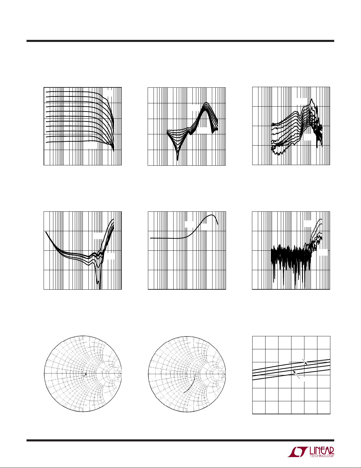
TYPICAL PERFORMANCE CHARACTERISTICS
Electrical Performance in Test Circuits A and B at TA = 25°C and VCC = 3.3V unless otherwise noted.
Differential Gain (Sdd21) vs
Frequency Over 11 Gain Settings
20
10
0
GAIN (dB)
–10
G
–20
–30
1 100 1000 10000
10
FREQUENCY (MHz)
MIN
Differential Input Match (Sdd11)
vs Frequency Over 11 Gain Settings
0
–10
G
MAX
Common Mode Gain (Scc21) vs
Frequency Over 11 Gain Settings
G
MAX
6412 G01
20
0
–20
GAIN (dB)
–40
–60
–80
1 100 1000 10000
10
FREQUENCY (MHz)
G
MAX
G
MIN
6412 G02
CM-to-DM Gain (Sdc21) vs
Frequency Over 11 Gain Settings
0
G
–20
–40
GAIN (dB)
–60
–80
1 100 1000 10000
10
FREQUENCY (MHz)
MAX
G
MIN
6412 G03
Differential Reverse Isolation
Differential Output Match (Sdd22)
vs Frequency Over 11 Gain Settings
0
G
MAX
G
–10
MIN
(Sdd12) vs Frequency Over 6 Gain
Settings
–40
G
MAX
–60
–20
RETURN LOSS (dB)
–30
–40
1 100 1000 10000
10
FREQUENCY (MHz)
Differential Input Smith Chart
(Sdd11) 10MHz to 500MHz Over 6
Gain Settings
ZO = 50Ω
G
MIN
G
MAX
6412 G07
G
MIN
6412 G04
–20
RETURN LOSS (dB)
–30
–40
1 100 1000 10000
10
FREQUENCY (MHz)
6412 G05
–80
ISOLATION (dB)
–100
–120
1 100 1000 10000
10
FREQUENCY (MHz)
G
MIN
6412 G06
Differential Output Smith Chart
(Sdd22) 10MHz to 500MHz Over 6
Gain Settings
= 200Ω
Z
O
10MHz
G
120MHz
MAX
240MHz
G
MIN
380MHz
500MHz
6412 G08
Supply Current vs Supply Voltage
Over Temperature
120
115
30°C
110
105
100
TOTAL SUPPLY CURRENT (mA)
95
90
3.0
85°C
–40°C
3.2 3.3 3.4
3.1
SUPPLY VOLTAGE (V)
0°C
3.5 3.6
6412 G09
6412fa
8
Page 9

TYPICAL PERFORMANCE CHARACTERISTICS
Electrical Performance in Test Circuits A and B at TA = 25°C and VCC = 3.3V unless otherwise noted.
Gain (Sdd21) Conformance Error
Differential Gain (Sdd21) vs
Control Voltage Over Temperature
20
15
10
5
0
GAIN (dB)
–5
–10
–15
–20
0
–VG: NEGATIVE
SLOPE MODE
FREQ = 140MHz
–40°C
25°C
85°C
0.2 0.4 0.8
+VG OR –VG VOLTAGE (V)
0.6
+VG: POSITIVE
SLOPE MODE
1.0
6412 G10
1.2
vs Control Voltage Over
Temperature
5
FREQ = 140MHz
4
3
2
0.2
–40°C
85°C
0.6 0.8
0.4
–VG VOLTAGE (V)
1
0
–1
–2
–3
GAIN CONFORMANCE ERROR (dB)
–4
G
MAX
–5
0
25°C
1.0
G
MIN
6412 G11
20
15
(DEG)
10
MAX
5
0
–5
–10
–15
sdd21 PHASE RELATIVE TO G
1.2
–20
LTC6412
Relative Phase (Sdd21)
vs Control Voltage Over Frequency
400MHz
200MHz
PHASE
ADV.
100MHz
PHASE
DELAY
G
MAX
0.2 0.4 0.8
0
–VG VOLTAGE (V)
0.6
1.0
G
MIN
6412 G12
1.2
Output IP3 at 140MHz vs Control
Voltage Over Temperature
45
40
35
P
= –6dBm/TONE
OUT
30
ΔFREQ = 1MHz
25
OIP3 (dBm)
20
15
10
–40°C
25°C
85°C
G
MAX
0.8 1.2
0
0.2
0.6 1.0
0.4
–VG VOLTAGE (V)
Output IP3 vs Control Voltage
Over Tone Spacing
45
40
35
P
= –6dBm/TONE
OUT
30
FREQ = 140MHz
SPACING =
25
OIP3 (dBm)
20
15
10
0.5MHz
1MHz
2MHz
5MHz
G
MAX
0.8 1.2
0
0.2
0.6 1.0
0.4
–VG VOLTAGE (V)
G
MIN
6412 G13
G
MIN
6412 G16
Output IP3 vs Control Voltage
Over Frequency
45
0.2
70MHz
140MHz
240MHz
380MHz
P
= –6dBm/TONE
OUT
ΔFREQ = 1MHz
0.6 1.0
0.4
–VG VOLTAGE (V)
40
35
30
25
OIP3 (dBm)
20
15
G
10
0
MAX
Output IP3 vs Control Voltage
Over Output Power per Tone
45
40
35
TEST EQUIPMENT LIMITED
30
FREQ = 140MHz
25
ΔFREQ = 1MHz
OIP3 (dBm)
=
P
OUT
20
15
10
G
0
MAX
0.2
–6dBm/TONE
–3dBm/TONE
–9dBm/TONE
0.4
–VG VOLTAGE (V)
0.6 1.0
G
0.8 1.2
INPUT
ATTENUATOR
LIMITED
G
0.8 1.2
MIN
6412 G14
MIN
6412 G17
Output IP3 at 140MHz
vs Control Voltage Over V
45
40
35
P
= –6dBm/TONE
OUT
30
ΔFREQ = 1MHz
25
OIP3 (dBm)
20
15
10
3.6V
3.3V
3V
G
MAX
0
0.2
0.4
–VG VOLTAGE (V)
3rd Harmonic Distortion
vs Control Voltage Over V
–20
FREQ = 140MHz
= 0dBm
P
OUT
–40
–60
VCC = 3V
HD3 (dBc)
–80
VCC = 3.6V
–100
G
MAX
–120
0
0.4 0.6 0.8
0.2
–VG VOLTAGE (V)
CC
0.8 1.2
0.6 1.0
CC
VCC = 3.3V
1.0 1.2
G
MIN
6412 G15
G
MIN
6412 G18
6412fa
9
Page 10

LTC6412
TYPICAL PERFORMANCE CHARACTERISTICS
Electrical Performance in Test Circuits A and B at TA = 25°C and VCC = 3.3V unless otherwise noted.
2nd Harmonic vs Distortion vs
Control Voltage Over Frequency
–20
P
= 0dBm
OUT
–40
–60
HD2 (dBc)
–80
–100
–120
G
MAX
0
0.2
FREQ = 280MHz
FREQ = 140MHz
FREQ = 70MHz
0.4 0.6 0.8
–VG VOLTAGE (V)
2nd Harmonic Distortion vs
Control Voltage Over P
–20
FREQ = 140MHz
POUT = 3dBm
OUT = 0dBm
G
0
MAX
0.2
P
OUT = –3dBm
P
0.4 0.6 0.8
–VG VOLTAGE (V)
ATTENUATOR
–40
–60
HD2 (dBc)
–80
–100
–120
OUT
LIMITED
1.0 1.2
INPUT
1.0 1.2
G
MIN
6412 G19
G
MIN
6412 G22
3rd Harmonic Distortion vs
Control Voltage Over Frequency
–20
P
= 0dBm
OUT
–40
–60
FREQ = 280MHz
HD3 (dBc)
–80
FREQ = 70MHz FREQ = 140MHz
–100
G
MAX
–120
0
0.4 0.6 0.8
0.2
–VG VOLTAGE (V)
3rd Harmonic Distortion vs
Control Voltage Over P
–20
FREQ = 140MHz
–40
–60
HD3 (dBc)
–80
–100
–120
0
P
= 3dBm
OUT
P
= –3dBm P
OUT
G
MAX
0.2
0.4 0.6 0.8
–VG VOLTAGE (V)
ATTENUATOR
OUT
OUT
LIMITED
= 0dBm
1.0 1.2
INPUT
1.0 1.2
G
MIN
6412 G20
G
MIN
6412 G23
Noise Figure at G
MAX
Frequency Over Temperature
14
12
10
8
6
NOISE FIGURE (dB)
4
2
0
50 150 350
0
100 200 400
85°C
25°C
–40°C
FREQUENCY (MHz)
140MHz Noise Figure vs Gain
Setting Over Temperature
45
40
35
30
25
20
15
NOISE FIGURE (dB)
10
5
0
–20
–15
–10
85°C
–40°C
0
–5
GAIN SETTING (dB)
vs
250
300
6412 G21
25°C
5
10
15
6412 G24
20
Output P
Over Supply Voltage
20
18
16
14
12
10
8
6
OUTPUT P1dB (dBm)
4
2
0
0
50 150
10
at G
1dB
3.6V
3.3V
3V
100
200
FREQUENCY (MHz)
vs Frequency
MAX
300
250
350
6412 G25
400
Input and Output P
Setting at 140MHz
20
INPUT P1dB
15
10
5
P1dB (dBm)
0
INPUT
ATTENUATOR
LIMITED
–5
–20
–15 –10
vs Gain
1dB
OUTPUT P1dB
OUTPUT
AMPLIFIER
LIMITED
0
–5 5 20
GAIN SETTING (dB)
10 15
6412 G26
140MHz Sideband Noise Near
G
at P
MAX
0
GAIN = G
–20
–40
–60
–80
–100
POWER DENSITY (dBc/Hz)
–120
–140
–20000 20000
= +8dBm
OUT
– 2dB
MAX
–10000 100000
OFFSET FROM 140MHz (Hz)
6412 G27
6412fa
Page 11

TYPICAL PERFORMANCE CHARACTERISTICS
Electrical Performance in Test Circuits A and B at TA = 25°C and VCC = 3.3V unless otherwise noted.
LTC6412
6dB Gain Control Step
70MHz Time Domain Response
–VG(0.25V/DIV)
RF
OUT
50Ω
VOLTAGE (V)
PEAK
RF
= 4dBm
OUT
012345
SHDN Step at G
TIME (μs)
with EN = 0V
MAX
6412 G28
70MHz Time Domain Response
SHDN (1V/DIV)
RF
OUT
50Ω
VOLTAGE (V)
PEAK RF
0 100 200 300 400 500
TIME (μs)
OUT
= 4dBm
6412 G31
10dB Gain Control Step
70MHz Time Domain Response
–VG(0.5V/DIV)
RF
OUT
50Ω
VOLTAGE (V)
012345
TIME (μs)
PEAK
RF
= 4dBm
OUT
SHDN Step at G = 3dB with EN = 0V
70MHz Time Domain Response
SHDN (1V/DIV)
RF
OUT
50Ω
VOLTAGE (V)
PEAK RF
0 100 200 300 400 500
TIME (μs)
OUT
= 4dBm
6412 G32
6412 G29
COMPRESSION
PEAK GAIN
20dB
10dB
VOLTAGE (V)
0dB
20dB Gain Control Step
70MHz Time Domain Response
–VG(0.5V/DIV)
RF
OUT
50Ω
VOLTAGE (V)
012345
TIME (μs)
Overdrive Compression at G
PEAK
RF
= 4dBm
OUT
6412 G30
MAX
70MHz Time Domain Response
RF
50Ω
OUT
020
PEAK RF
40 60 80 100
TIME (μs)
OUT
= 14dBm
6412 G33
Overdrive Recovery at G
70MHz Time Domain Response
1.2
1.0
0.8
0.6
0.4
0.2
VOLTAGE (V)
0
–0.2
–0.4
–0.6
0
EXTERNAL
RF SWITCH PULSE
RF
10dB ATTENUATED
15dB COMPRESSED
50
100
150
TIME (ns)
INTO 50Ω,
OUT
SMALL SIGNAL
200
250
RF
MAX
PEAK
OUT
300
= 14dBm
350
6412 G34
400
Output EN Step at G
MAX
140MHz Time Domain Response
2.5
2.0
1.5
1.0
0.5
VOLTAGE (V)
0
–0.5
–1.0
–1.5
0
EN
RF
OUT
50Ω
PEAK RF
40 80 120 20014020 60 100 180
TIME (ns)
OUT
= 10dBm
160
6412 G35
SHDN Supply Current
Time Domain Response
120
100
80
60
40
20
SUPPLY CURRENT (mA)
0
1.00.5
0
2.01.5
2.5
TIME (ms)
3.0 3.5 4.5
4.0
6412 G36
3.0
2.0
1.0
0
5.0
SHDN PIN VOLTAGE (V)
6412fa
11
Page 12

LTC6412
PIN FUNCTIONS
GND (Pins 1, 8, 12, 15, 18, 20, 23): Ground. Pins are
connected to each other internally. For best RF performance,
all ground pins should be connected to the printed circuit
board ground plane.
+IN (Pin 2): Positive Signal Input Pin. Has an internally generated DC Bias. A 10nF DC blocking capacitor is
recommended.
–IN (Pin 3): Negative Signal Input Pin. Has an internally generated DC Bias. A 10nF DC blocking capacitor is
recommended.
(Pins 4, 5): Input Common Mode Voltage Pins. Two
V
CM
pins are tied together internally and serve as a virtual
ground for the differential inputs, +IN and –IN. Capacitive decoupling to ground with 10nF close to the pins is
recommended to help terminate any residual common
mode input signal.
(Pins 6, 13, 19, 24): Positive Power Supply. All
V
CC
four pins must be tied to the same voltage, usually 3.3V.
Bypass each pin with 1000pF and 0.1μF capacitors close
to the pins.
DECL1 (Pin 7): Decoupling Pin. Serves to reduce internal
noise. Bypass to ground with a 0.1μF capacitor close to
the pin.
(Pin 9): Positive Gain Control Pin. Input signal pin used
+V
G
for positive mode gain control. Otherwise, pin is typically
connected to V
for negative mode gain control. Pin is
REF
internally pulled to ground with a 10k resistor. In positive
gain slope mode, the gain control slope is approximately
+32dB/V at 140MHz with a gain control range of 0.1V to
1.1V.
(Pin 10): Internal Bias Voltage Pin. Typically tied to
V
REF
pin for positive gain control or tied to +VG for nega-
–V
G
tive gain control. Determines the midpoint voltage of the
gain-vs-V
characteristic. Bypass to ground with 0.1μF
G
capacitor close to the pin. Not intended for use as an
external reference voltage.
(Pin 11): Negative Gain Control Pin. Input signal pin
–V
G
used for negative mode gain control. Otherwise, pin is
typically connected to V
for positive mode gain con-
REF
trol. Pin is internally pulled to ground with a 10k resistor.
In negative gain slope mode, the gain control slope is
approximately –32dB/V at 140MHz with a gain control
range of 0.1V to 1.1V.
DECL2 (Pin 14): Decoupling Pin. Serves to reduce internal
noise. Bypass to ground with a 1000pF capacitor close
to the pin.
–OUT (Pin 16): Negative Amplifi er Output Pin. A transformer with a center tap tied to V
or a choke inductor
CC
is recommended to conduct DC quiescent current to the
open-collector output device. For best performance, DC
bias voltage to –OUT must be within 100mV of V
CC
.
+OUT (Pin 17): Positive Amplifi er Output Pin. A transformer with a center tap tied to V
or a choke inductor
CC
is recommended to conduct DC quiescent current to the
open-collector output device. For best performance, DC
bias voltage to +OUT must be within 100mV of V
CC
.
EN (Pin 21): Output Signal Enable Pin. Pin is internally
pulled high with 100kΩ to V
. Assert pin to a low volt-
CC
age to enable the output amplifi er signal. Output amplifi er
impedance and DC current are not affected by the EN state.
Connect pin to ground if enable function is not used.
SHDN (Pin 22): Shutdown Pin. Pin is internally pulled high
with 100kΩ to V
. Assert pin to a low voltage to shut
CC
down the circuit and greatly reduce the supply current.
Proper sequencing of the EN and SHDN pins is required
to avoid non-monotonic output signal behavior. See
Applications Information section for details. Connect pin
if shutdown function is not used.
to V
CC
Exposed Pad (Pin 25): Ground. The Exposed Pad should
have multiple via holes to an underlying ground plane for
low inductance and good thermal dissipation.
12
6412fa
Page 13

BLOCK DIAGRAM
222419136
V
V
V
CC
CC
REFERENCE AND BIAS CONTROL
CC
CC
SHDN
LTC6412
15
21
EN
23
GNDV
GND
DC TEST CIRCUIT
= (+IN) – (–IN)
V
IN(DIFF)
V
= [(+IN) + (–IN)]/2
IN(CM)
+IN
2
–IN
3
V
CM
4
V
CM
5
0.1μF
+IN
–IN
ATTENUATOR
CONTROL
+V
V
G
9
V
+IN
–IN
REF
10
CC
0.1μF
CC
CM
V
DECL1
GND V
0.1μF 0.1μF
11 1
2.2V 0.8V
LTC6412
DECL2
–V
G
SHDN
0.1μF
• • •
• • •
• • •
GND
EN
REF
G
V
+V
BUFFER/
OUTPUT
AMPLIFIER
REFERENCE AND
BIAS CONTROL
GND12GND15GND
8
≈ VCC + 2.3V
V
SUPPLY
+OUT
–OUT
G
–V
V
≈ VCC + 2.3V
SUPPLY
GND
18
100Ω
100Ω
EXPOSED
+OUT
–OUT
PAD
25
V
OUT(DIFF)
V
OUT(CM)
+OUT
–OUT
DECL1
DECL2
6412 BD
17
16
7
14
= (+OUT) – (–OUT)
= [(+OUT) + (–OUT)]/2
6412 TC
GAIN CONTROL
(NEGATIVE SLOPE)
6412fa
13
Page 14

LTC6412
OPERATION
The LTC6412 employs an interpolated, tapped attenuator
circuit architecture to generate the variable-gain characteristic of the amplifi er. The tapped attenuator is fed to a
buffer and output amplifi er to complete the differential
signal path shown in the Block Diagram. This circuit
architecture provides good RF input power handling capability along with a constant output noise and output IP3
characteristic that are desirable for most IF signal chain
applications. The internal control circuitry takes the gain
control signal from the ±V
terminals and converts this
G
to an appropriate set of control signals to the attenuator
ladder. The attenuator control circuit ensures that the
linear-in-dB gain response is continuous and monotonic
over the gain range for both slow and fast moving input
control signals while exhibiting very little input impedance
variation over gain. These design considerations result
in a gain-vs-V
characteristic with a ±0.1dB ripple and
G
a 0.5μs gain response time that is slower than a similar
digital step attenuator design.
An often overlooked characteristic of an analog-controlled
VGA is upconverted amplitude modulation (AM) noise
from the gain control terminals. The VGA behaves as a
2-quadrant multiplier, so some minimal care is required
to avoid excessive AM sideband noise generation. The
following table demonstrates the effect of the baseline
20nV/√Hz equivalent input control noise from the LTC6412
circuit along with the effect of a higher combined input
noise due to a noisy external control circuit.
CONTROL INPUT TOTAL NOISE
VOLTAGE (nV/√Hz)
20 –142
40 –136
70 –131
100 –128
200 –122
PEAK AM NOISE AT 10kHz OFFSET
NEAR MAXIMUM GAIN (dBc/Hz)
The baseline equivalent 20nV/√Hz input noise is seen to
produce worst-case AM sidebands of –142dBc/Hz which is
near the –147dBm/Hz output noise fl oor at maximum gain
for a nominal 0dBm output signal. An input control noise
voltage less than 80nV/√Hz is generally recommended to
avoid measurable AM sideband noise. While op amp control
circuit output noise voltage is usually below 80nV/√Hz,
some low power DAC outputs exceed 150nV/√Hz. DACs
with output noise in the range of 100nV/√Hz to 150nV/√Hz
can usually be accommodated with a suitable 2:1 or 3:1
resistor divider network on the DAC output to suppress the
noise amplitude by the same ratio. Noisy DACs in excess
of 150nV/√Hz should be avoided if minimal AM noise is
important in the application.
14
6412fa
Page 15

APPLICATIONS INFORMATION
LTC6412
Introduction
The LTC6412 is a high linearity, fully-differential analogcontrolled variable-gain amplifi er (VGA) optimized for
application frequencies in the range of 1MHz to 500MHz.
The VGA architecture provides a constant OIP3 and constant
output noise level (NF + Gain) over the 31dB gain-control
range and thus exhibits a uniform spurious-free dynamic
range (SFDR) over gain. This constant SFDR characteristic
is ideal for use in receiver IF chains that are upstream from
a signal sink such as a demodulator or ADC.
The low supply voltage requirements and fully differential
design are compatible with many other LTC mixer, amplifi er
and ADC products for use in compact, low voltage, fully
differential receiver chains. For non-differential systems,
the 50Ω input impedance and 200Ω output impedance
are easily converted to single-ended 50Ω ports with
inexpensive 1:1 and 4:1 baluns.
Gain Characteristics
The LTC6412 provides a continuously adjustable gain range
of –14dB to 17dB that is linear-in-dB with respect to the
control voltages applied to +V
and –VG. These control
G
pins can be operated with a differential signal, but it is more
common to operate one of the V
control signal while connecting the other V
provided V
pin. In this way, either a positive gain-control
REF
pins with a single-ended
G
pin to the
G
slope or negative gain-control slope is easily achieved:
Negative Gain-Control Slope. Tie +V
gain control voltage to the –V
increasing –V
voltage.
G
pin. Gain decreases with
G
to V
G
and apply
REF
Port Characteristics
The LTC6412 provides a nominal 50Ω differential input
impedance and 200Ω differential output impedance over
the operating frequency range.
The input impedance characteristic derives from the
differential attenuator ladder shown in the Block Diagram.
The internal circuit controls the RF connections to this
attenuator ladder and generates the appropriate common
mode DC voltage to this port. The differential attenuator
ladder creates a virtual ground node that needs a capacitor
bypass to ground at the V
pin to effectively attenuate
CM
any common mode signal presented to the input port.
The +V
and –VIN pins are connected to the input signal
IN
through DC blocking capacitors as shown in Test Circuit A
and Test Circuit B, Figures 1-4.
The output impedance characteristic derives from the opencollector equivalent circuit shown in Figure 7. The action of
the differential shunt, lowpass fi lter, and internal feedback
presents an effective differential output impedance of
200Ω to 300Ω between the +OUT and –OUT pins over the
operating band. The +V
OUT
and –V
pins are connected
OUT
to the output port using shunt inductors or a transformer
to provide a DC path to the supply voltage. The DC block
to the circuit output is usually accomplished using series
capacitors. These blocking capacitors can be avoided if a
fl ux transformer is used at the output. Figure 9 illustrates
a few common inductor and balun transformer methods
for coupling the AC signal and DC supply to the output
pins. This is discussed further in the Typical Application
Circuits section.
Positive Gain-Control Slope. Tie –V
gain control voltage to the +V
increasing +V
voltage.
G
pin. Gain increases with
G
to V
G
and apply
REF
When connected in this typical single-ended confi guration,
the active control input range extends from 0.1V to 1.1V.
This control input range can be extended using a resistor
divider with a suitably low output resistance. For example,
two series resistors of 1k each would extend the control
input range from 0.2V to 2.2V while providing an effective
500Ω Thevinin equivalent source resistance, a relatively
small loading effect compared to the 10k input resistance
of the +V
/–VG terminals.
G
Power Supplies
Inductance to the supply path can degrade the performance
of the LTC6412. It is recommended that low inductance
bypass capacitors are installed very close to each of
the V
pins. 1000pF and 0.1μF parallel capacitors are
CC
recommended with the smaller capacitor placed closer to
the V
pin. Do not leave any supply pins disconnected. For
CC
best performance, DC bias voltage to the +OUT and –OUT
pins must be within 100mV of V
. The Exposed Pad on
CC
the underside of the package must be connected to ground
with low inductance and low thermal resistance. Refer to
details of DC1464A (Test Circuit A) for an example of proper
6412fa
15
Page 16

LTC6412
APPLICATIONS INFORMATION
grounding and supply decoupling. Failure to provide low
impedance supply and ground at high frequencies can
cause oscillations and increased distortion.
Enable/Shutdown
Both the EN pin and SHDN pin are self-biased to V
through
CC
their respective 100k pull-up resistors, so the default
open-pin state is powered on with the output amplifi er
signal path disabled. Pulling the EN pin low completes
the signal path from the attenuator ladder through the
output amplifi er. The EN pin essentially provides a fast
muting function while the SHDN pin provides slower
power on/off function.
For applications requiring the SHDN function, it is
recommended that the output amplifi er signal path be
disabled with a high EN voltage before transitioning the
SHDN signal. When enabling the amplifi er, allow at least
5ms dwell time between the rising SHDN transition and the
falling EN transition to avoid non-monotonic output signal
behavior though the VGA. The opposite delay sequence
is recommended for the falling SHDN transition, but this
is less critical as the output signal amplitude will drop
abruptly regardless of the EN pin.
SHDN
t
DWELL
EN
t
DWELL
6412 AI01
The topside metal and silkscreen drawings for Test Circuit A
illustrate the recommended decoupling capacitor placement, signal routing and grounding. Ground vias directly
beneath the Exposed Pad are critical; use as many as possible.
Ground vias to the other ground pins are less critical.
ESD
The LTC6412 is protected with reverse-biased ESD diodes
on all I/O pins. If any I/O pin is forced one diode drop above
the positive supply or one diode drop below the negative
supply, then large currents may fl ow through the diodes.
No damage to the devices will occur if the current is kept
below 10 mA. The +OUT/–OUT pins have additional series
diodes to the positive supply and can sustain approximately
2V overshoot above the positive supply before conducting
appreciable currents.
Signal Compression Characteristics
The graph entitled, Input and Output P1dB, illustrates
an important characteristic of the LTC6412 VGA. At gain
settings above –5dB, the output amplifi er limits the linear
power handling capability, but at gain settings below
–5dB, the input attenuator ladder limits the linear power
handling capability. The linear input power limitations at
minimum gain do not affect the overall performance of
a signal chain if the preceding mixer or amplifi er stage
exhibits an OP1dB < 19dBm and an OIP3 < 50dBm.
Test Circuits
Layout/Grounding
The high frequency performance of the LTC6412 requires
special attention to proper RF grounding, bias decoupling
and termination. The recommended PCB stack-up for a
4-layer board is shown below for 1oz copper clad FR-4
laminate with a relative dielectric constant, ε
= 4.2-4.5
r
at 1GHz.
METAL 1
FR4 12-18 MILS
METAL 2
FR4 20-30 MILS
METAL 3
FR4 NOT CRITICAL
METAL 4
6412 AI02
RF SIGNAL
GROUND PLANE
POWER PLANE
GND AND LF SIGNAL
16
The fully-differential nature of the LTC6412 design requires
two test circuits to generate the performance information
presented in this data sheet.
Test Circuit A is DC1464A, a 2-port demonstration circuit
with input/output balun transformers to allow for direct
connection to a 2-port network analyzer or other singleended 50Ω test system. The balun transformers limit the
high and low frequency performance of the LTC6412 but
allow for simple and reasonably accurate measurements
from 70MHz to 380MHz. The gain control signal is supplied
to either of the V
or through the V
turrets for DC control measurements
G
SMA connector for transient control
GAIN
signal measurements. Clip leads to the gain control turrets
are susceptible to noise pickup and should be lowpass
6412fa
Page 17

APPLICATIONS INFORMATION
LTC6412
fi ltered to avoid AM upconversion artifacts. While using
the ±V
input to ground provides an effective lowpass fi lter.
Typical data curves quoted for Test Circuit A are measured
at the plane of the SMA connectors and are NOT corrected
for any losses introduced by the input and output baluns,
estimated at approximately 0.5dB and 1.2dB, respectively.
All typical AC data reported in this data sheet correspond
to Test Circuit A, except for mixed-mode S-parameters of
the form Sdd21, Scc21, etc.
Test Circuit B uses a 4-port network analyzer to measure
differential mode and common mode S-parameters
beyond the frequency limitations imposed by the balun
transformers and associated circuitry. A matching
calibration set establishes the measurement reference
planes shown in Test Circuit B. The output plane is defi ned
at the edge of the package while the input plane is defi ned
at the edge of the input pair of 0402 capacitors. The IC
land and ground via pattern are identical to that shown
for Test Circuit A. The ground via pattern directly beneath
the package is critical to provide the proper RF ground to
produce the RF characteristics quoted in this data sheet.
All mixed-mode S-parameter typical data curves of the
form SxyAB correspond to Test Circuit B following the
defi nitions described in Figures 5 and 6.
turrets, a 4.7μF capacitor from the V
G
GAIN
SMA
electrical characteristics such as low loss, broad band
response and good phase matching.
6412 F01
Typical Application Circuits
Grounding and supply decoupling should closely follow the
suggested layout shown for Test Circuit A, but the input
and output networks can be customized to suit various
application requirements.
On the input side, the differential port impedance is
very close to 50Ω over all gain settings and application
frequencies. In a differential signal chain, the differential
input signal is easily supplied from a preceding differential
output stage with a suitable DC blocking capacitor of
approximately 10nF. If the system employs a single-ended
input signal to the VGA, then a suitable balun is required
to convert to a differential input signal. The passive
conversion from 50Ω single-ended to 50Ω differential is
most effectively accomplished with a 1:1 transmission-line
balun such as the ETC1-1-13 or MABA-007159. These 1:1
balun devices are relatively inexpensive and offer excellent
Figure 1. Top Silkscreen for DC1464A. Test Circuit A
On the output side, the differential port admittance is very
close to 300Ω||1.5pF across all gain settings and application
frequencies. This output port circuit must provide a path for
DC output supply current as well as any balun, matching,
or fi ltering functions required by the application. Thus, the
design options for the output circuitry are more varied. A
brief list of the more common output circuits is shown in
Figure 9 along with a few design guidelines to estimate
component values. Final design simulations should use the
small-signal equivalent circuit model in Figure 8 to properly
account for loading effects of the output terminals.
Figure 9a shows the simplest differential output
confi guration employing two suitable inductors, L1 = L2,
to pass the DC supply current without loading the output
nodes at the application frequency. The PCB trace widths
6412fa
17
Page 18

LTC6412
APPLICATIONS INFORMATION
Figure 9b shows a further variation of the tuned differential
output where the DC blocking capacitors are brought inside
the tank resonator to participate in the bandpass fi lter and
transform the VGA output impedance to a lower value.
Here too, the C
shunt capacitors to ground, so any common mode noise
is fi ltered as well.
Figure 9c shows a fl ux transformer used to achieve a
50Ω single-ended output. The fl ux transformer does
not provide the large bandwidth typical of the output
transmission-line transformer shown in Figure 3, but it
usually performs well over smaller bandwidths, especially
when tuned with shunt capacitors (not shown). The fl ux
transformer design eliminates DC blocking capacitors and
is attractive in rugged applications where the amplifi er
output is subjected to ESD events and other forms of
transient electrical overstress that do not pass through a
typical RF fl ux transformer such as the MABAES0061.
capacitor can be split into two separate
O
6412 F02
Figure 2. Top Metal for DC1464A. Test Circuit A
from the output pins should be narrow in keeping with
the high impedance of these terminals; 8 to 10mil trace
width on 1oz copper is a good choice. The 0.1μF capacitors
serve to DC block and decouple as needed. These capacitor
values are adequate down to a few MHz and can be scaled
down for higher application frequencies.
If bandpass fi ltering is needed at the VGA output of
Figure 9a, then L1 and L2 can be designed to resonate
with a shunt capacitor, C
ω =1/√C
to resonate with two separate capacitors, C1 = C2, so any
common mode noise is fi ltered as well.
(L1 + L2). Alternately, L1 = L2 can be designed
O
, at the frequency of interest,
O
Figure 9d shows a discrete LC balun suitable for bandwidths
of approximately 15% to 30%. Larger bandwidths are
diffi cult to achieve with the number of components shown,
and smaller bandwidths are often limited by component
tolerance effects. Despite these limitations, the discrete
LC balun can be a cost effective output circuit solution.
At resonance, the tuned circuit produces an impedance
transformation along with the differential-to-single-ended
conversion.
DC-Coupled Operation
The LTC6412 is intended for AC-coupled operation. The
translation between the fi xed input DC common mode
voltage and higher open-collector output DC bias point
makes it impractical to use in DC-coupled applications.
18
6412fa
Page 19

APPLICATIONS INFORMATION
V
CC
C3 0.1μF
C2 1000pF
LTC6412
SHDN EN
V
CC
R1
1k
R3
[1]
R5
1k
V
CC
R2
[1]
V
CC
R4
C4 0.1μF
1k
R6
1k
C2 1000pF
+IN
–IN
R7
[1]
R9
0Ω
V
3.00V TO 3.60V
GND
5
40dB
CC
NOTE:
[1] DO NOT PLACE
C5
T1
1
1:1
••
2
3
C11
10nF
V
CC
CB1
4.7μF
CA1
1μF
10nF
C8
10nF
V
CC
C14
0.1μF
C17
0.1μF
TEST IN TEST OUT
C13
1000pF
R21
0Ω
24 23 22 21 20 19
VCCGND SHDN
1
GND
2
+IN
3
–IN
4
V
5
V
6
V
DECL1
+V
G
T3
5
1:1
4
LTC6412
CM
CM
CC
GND +VGV
789101112
R15 0Ω
R17
100Ω
R18 [1]
13
••
2
3
EN GND V
REF–VG
R14 [1]
R19 0Ω
C18 0.1μF
C19 0.1μF
C22
0.1μF
V
GAIN
CC
GND
+OUT
–OUT
GND
DECL2
V
GND
2
1
18
17
16
15
14
13
CC
R20
100Ω
••
T2
4:1
3
V
C7 0.1μF
C16
1000pF
–V
G
T4
1:1
CC
2
1
•
V
CC
BALUN
T1, T3, T4
4
5
R22
0Ω
6412 F03
C12
1000pF
C15
0.1μF
PART NUMBER
TYCO MABA-007159
T2
MINI-CIRCUITS TCM4-19+
4
5
C20
[1]
C21
0.1μF
C6
0.1μF
C9
[1]
+OUT
–OUT
Figure 3. Demo Board DC1464A Circuit Schematic. Test Circuit A
10nF
10nF
10nF
+IN
–IN
3.3V
GND
CC
V
LTC6412
CM
V
SHDN
DECL2
DECL1
0.1μF
1nF
OUTPUT REF
PLANE
0.1μF
I
+OUT
EN
G
–V
REF
G
V
–OUT
+V
DC
I
DC
GAIN CONTROL
(– SLOPE MODE)
0.1μF0.1μF
INPUT REF
PLANE
1/2 AGILENT
E5071C
PORT 1
50Ω
PORT 2
50Ω
Figure 4. 4-Port Analysis Schematic. Test Circuit B
1/2 AGILENT
E5071C
PORT 3
50Ω
PORT 4
50Ω
6412 F04
6412fa
19
Page 20

LTC6412
APPLICATIONS INFORMATION
DIFFERENTIAL
MODE
PORT 1
50Ω
TRANSFORMER WITH CENTER TAP
COMMON
MODE
PORT 1
1:1
IDEAL
COMMON
MODE
PORT 2
+OUT+IN
DUT
–OUT–IN
50Ω12.5Ω
TRANSFORMER WITH CENTER TAP
DIFFERENTIAL
PORT 2
1:1
IDEAL
MODE
200Ω
6412 F05
Figure 5. Schematic of Mixed-Mode S-Parameters Reported for Test Circuit B
S xyAB
STIMULUS PORT NUMBER
RESPONSE PORT NUMBER
STIMULUS PORT MODE
RESPONSE PORT MODE
d: DIFFERENTIAL MODE (BALANCED)
MODE
c: COMMON MODE (BALANCED)
S xyAB =
x MODE SIGNAL OUTPUT ON PORT A
y MODE SIGNAL INPUT ON PORT B
6412 F06
Figure 6. Defi nition of Mixed-Mode S-Parameters Reported for Test Circuit B
IDEAL 1:1
TRANSFORMER
WITH
CENTER TAP
1.5pF
190Ω
5pF 4pF
175Ω
6412 F08
1nH
1nH
+OUT
–OUT
Z
OUT
TO BUFFER
AMP
5Ω 5Ω
8pF
0.3pF
5Ω 5Ω
LOWPASS FILTER
150Ω0.3pF
150Ω
6412 F06
+OUT
gm300Ω
DIFFERENTIAL
MODE ADMITTANCE
COMMON MODE
ADMITTANCE
–OUT
Figure 7. Large-Signal Output Equivalent Circuit Schematic Figure 8. Small-Signal Output Equivalent Circuit Model
20
6412fa
Page 21

APPLICATIONS INFORMATION
LTC6412
(a)
(b)
(c)
+OUT
LTC6412
–OUT
+OUT
LTC6412
–OUT
+OUT
LTC6412
–OUT
10mil
LINE WIDTH
C1
0.1μF
L1 = L2
C1 = C2
Z
= 200Ω
OUT
DIFFERENTIAL
NOTE: DASHED LINE COMPONENTS
ARE FOR BANDPASS FILTERING
(SEE TEXT)
L1 = L2
C1 = C2
AT RESONANCE,
O
= 200Ω
Z
OUT
C1
DIFFERENTIAL
T2 = MABAES0061
= 50Ω
Z
OUT
SINGLE ENDED
2
1
C
O
1C21
1
++
C
O
0.1μF
0.1μF
4:1
L1
C
O
L2
C2
L1
L2
T2
0.1μF
C1
C
C2
V
CC
V
CC
V
CC
0.1μF
V
CC
(d)
0.1μF
+OUT
LTC6412
–OUT
L1
C1
L2
C2 LC
BALUN
6412 F09
L
CHOKE
0.1μF
L1 = L2 = L
C1 = C2 = C
1
=
X
C
C
2πf
O
AT RESONANCE,
Z
SINGLE ENDED
OUT
2
X
C
=
200Ω
fO =
2π√LC
Figure 9. Output AC/DC Coupling, Filter and Balun Circuit Design Options
1
6412fa
21
Page 22

LTC6412
PACKAGE DESCRIPTION
UF Package
24-Lead Plastic QFN (4mm × 4mm)
(Reference LTC DWG # 05-08-1697)
0.70 p0.05
4.50 p 0.05
3.10 p 0.05
2.45 p 0.05
(4 SIDES)
RECOMMENDED SOLDER PAD PITCH AND DIMENSIONS
4.00 p 0.10
(4 SIDES)
PIN 1
TOP MARK
(NOTE 6)
NOTE:
1. DRAWING PROPOSED TO BE MADE A JEDEC PACKAGE OUTLINE MO-220 VARIATION (WGGD-X)—TO BE APPROVED
2. DRAWING NOT TO SCALE
3. ALL DIMENSIONS ARE IN MILLIMETERS
4. DIMENSIONS OF EXPOSED PAD ON BOTTOM OF PACKAGE DO NOT INCLUDE
MOLD FLASH. MOLD FLASH, IF PRESENT, SHALL NOT EXCEED 0.15mm ON ANY SIDE, IF PRESENT
5. EXPOSED PAD SHALL BE SOLDER PLATED
6. SHADED AREA IS ONLY A REFERENCE FOR PIN 1 LOCATION
ON THE TOP AND BOTTOM OF PACKAGE
0.25 p0.05
0.50 BSC
PACKAGE OUTLINE
0.75 p 0.05
2.45 p 0.10
(4-SIDES)
0.200 REF
0.00 – 0.05
BOTTOM VIEW—EXPOSED PAD
R = 0.115
TYP
2423
PIN 1 NOTCH
R = 0.20 TYP OR
0.35 s 45o CHAMFER
0.40 p 0.10
1
2
(UF24) QFN 0105
0.25 p 0.05
0.50 BSC
22
6412fa
Page 23

LTC6412
REVISION HISTORY
REV DATE DESCRIPTION PAGE NUMBER
A 4/10 Change TC
Typical to –0.007dB/°C in DC Electrical Characteristics 3
GAIN
Information furnished by Linear Technology Corporation is believed to be accurate and reliable.
However, no responsibility is assumed for its use. Linear Technology Corporation makes no representation that the interconnection of its circuits as described herein will not infringe on existing patent rights.
6412fa
23
Page 24

LTC6412
RELATED PARTS
PART NUMBER DESCRIPTION COMMENTS
Fixed Gain IF Amplifi ers/ADC Drivers
LT1993-2, LT1993-4,
LT1993-10
LTC6400-8, LTC6400-14,
LTC6400-20, LTC6400-26
LTC6401-8, LTC6401-14,
LTC6401-20, LTC6401-26
LT6402-6, LT6402-12,
LT6402-20
LTC6410-6 1.4GHz Differential IF Amplifi er with Confi gurable
LTC6416 2GHz, 16-Bit Differential ADC Buffer –72dBc IM2 at 300MHz 2V
LTC6420-20 Dual 1.8GHz Low Noise, Low Distortion
LTC6421-20 Dual 1.3GHz Low Noise, Low Distortion
IF Amplifi ers/ADC Drivers with Digitally Controlled Gain
LT5514 Ultralow Distortion IF Amplifi er/ADC Driver with
LT5524 Low Distortion IF Amplifi er/ADC Driver with
LT5554 High Dynamic Range 7-Bit Digitally Controlled IF
Baseband Differential Amplifi ers
LT1994 Low Noise, Low Distortion Differential
LTC6403-1 Low Noise Rail-to-Rail Output Differential
LTC6404-1, LTC6404-2 Low Noise Rail-to-Rail Output Differential
LTC6406 3GHz Rail-to-Rail Input Differential Amplifi er/ADC
LT6411 Low Power Differential ADC Driver/Dual
Low Noise DAC for Gain Control
LTC2630-10 Low Power, Internal Reference, Single Supply
LTC2640-10 Low Power, Internal Reference, Single Supply
LTC2641-12 Low Noise, Low Power, Single Supply 12-Bit DAC SPI Input, Low Glitch Impulse, Power-On to Zero-Scale
LTC2642-12 Low Noise, Low Power, Single Supply 12-Bit DAC SPI Input, Low Glitch Impulse, Power-On to Mid-Scale
800MHz Differential Amplifi er/ADC Drivers –72dBc IM3 at 70MHz 2V
1.8GHz Low Noise, Low Distortion Differential
ADC Drivers
1.3GHz Low Noise, Low Distortion Differential
ADC Drivers
300MHz Differential Amplifi er/ADC Drivers –71dBc IM3 at 20MHz 2V
Input Impedance
Differential ADC Drivers
Differential ADC Drivers
Digitally Controlled Gain
Digitally Controlled Gain
VGA/ADC Driver
Amplifi er/ADC Driver
Amplifi er/ADC Driver
Amplifi er/ADC Driver
Driver
Selectable Gain Amplifi er
10-Bit DAC
10-Bit DAC
–71dBc IM3 at 240MHz 2V
20dB, 26dB
–74dBc IM3 at 140MHz 2V
20dB, 26dB
OIP3 = 36dBm at 70MHz, Flexible Interface to Mixer IF Port
AV = 0dB, 300MHz ±0.1dB Bandwidth
Dual Version of the LTC6400-20, A
Dual Version of the LTC6401-20, AV = 20dB
OIP3 = 47dBm at 100MHz, Gain Range 10.5dB to 33dB by 1.5dB
OIP3 = 40dBm at 100MHz, Gain Range 4.5dB to 37dB by 1.5dB
OIP3 = 46dBm at 200MHz, Gain Range 1.725 to 17.6dB by 0.125dB
16-Bit SNR, SFDR at 1MHz, Rail-to-Rail Outputs
16-Bit SNR, SFDR at 3MHz, Rail-to-Rail Outputs, e
16-Bit SNR, SFDR at 10MHz, Rail-to-Rail Outputs, eN = 1.5nV/√Hz,
LTC6404-1 is Unity-Gain Stable, LTC6404-2 is Gain-of-2 Stable
–65dBc IM3 at 50MHz 2V
e
= 1.6nV/√Hz, 18mA
N
–83dBc IM3 at 70MHz 2V
for Single-Ended to Differential Conversion
SPI Input, 2.5V Output Range, Resistor Divide Output by ~2:1
SPI Input, 2.5V Output Range, Resistor Divide Output by ~2:1
Composite, AV = 2V/V, 4V/V, 10V/V
P-P
Composite, IS = 90mA, AV = 8dB, 14dB,
P-P
Composite, IS = 50mA, AV = 8dB, 14dB,
P-P
Composite, AV = 6dB, 12dB, 20dB
P-P
Composite, IS = 42mA, eN = 2.8nV/√Hz,
P-P
= 20dB
V
= 2.8nV/√Hz
N
Composite, Rail-to-Rail Inputs,
P-P
Composite, AV = 1, –1 or 2, 16mA, Excellent
P-P
24
Linear Technology Corporation
1630 McCarthy Blvd., Milpitas, CA 95035-7417
(408) 432-1900 ● FAX: (408) 434-0507
●
www.linear.com
6412fa
LT 0410 REV A • PRINTED IN USA
© LINEAR TECHNOLOGY CORPORATION 2009
Page 25

 Loading...