

Page 1
FEATURES
–
LTC6240/LTC6241/LTC6242
Single/Dual/Quad 18MHz,
Low Noise, Rail-to-Rail Output,
CMOS Op Amps
U
DESCRIPTIO
■
0.1Hz to 10Hz Noise: 550nV
■
Input Bias Current:
P-P
0.2pA (Typ at 25°C)
1pA Max (LT6240)
■
Low Offset Voltage: 125µV Max
■
Low Offset Drift: 2.5µV/°C Max
■
Gain Bandwidth Product: 18MHz
■
Output Swings Rail-to-Rail
■
Supply Operation:
2.8V to 6V LTC6240/LTC6241/LTC6242
2.8V to ±5.5V LTC6240HV/LTC6241HV/LTC6242HV
■
Low Input Capacitance
■
H Grade Temperature Range: –40°C to 125°C
■
Single LTC6240 in 5-Pin SOT-23 Package and
8-Pin SO for PCB Guard Ring
■
Dual LTC6241 in 8-Pin SO and Tiny DFN Packages
■
Quad LTC6242 in 16-Pin SSOP and 5mm × 3mm
DFN Packages
U
APPLICATIO S
■
Photo Diode Amplifi ers
■
Charge Coupled Amplifi ers
■
Low Noise Signal Processing
■
Medical Instrumentation
■
High Impedance Transducer Amplifi er
The LTC®6240/6241/LTC6242 are single, dual and quad
low noise, low offset, rail-to-rail output, unity gain stable
CMOS op amps that feature 1pA of input bias current. Input
bias current is guaranteed to be 1pA max on the single
LTC6240. The 0.1Hz to 10Hz noise of only 550nV
, along
P-P
with an offset of just 125µV are signifi cant improvements
over traditional CMOS op amps. Additionally, noise is
guaranteed to be less than 10nV/√Hz at 1kHz. An 18MHz
gain bandwidth, and 10V/µs slew rate, along with the wide
supply range and low input capacitance, make them perfect
for use as fast signal processing amplifi ers.
These op amps have an output stage that swings within
30mV of either supply rail to maximize the signal dynamic
range in low supply applications. The input common mode
range extends to the negative supply. They are fully specifi ed on 3V and 5V, and an HV version guarantees operation
on supplies up to ±5V.
The LTC6240 is available in the 8-pin SO and the 5-pin
SOT-23 packages. The LTC6241 is available in the 8-pin
SO, and for compact designs it is packaged in a tiny dual
fi ne pitch leadless (DFN) package. The LTC6242 is available in the 16-Pin SSOP as well as the 5mm × 3mm DFN
package.
, LTC and LT are registered trademarks of Linear Technology Corporation.
All other trademarks are the property of their respective owners.
U
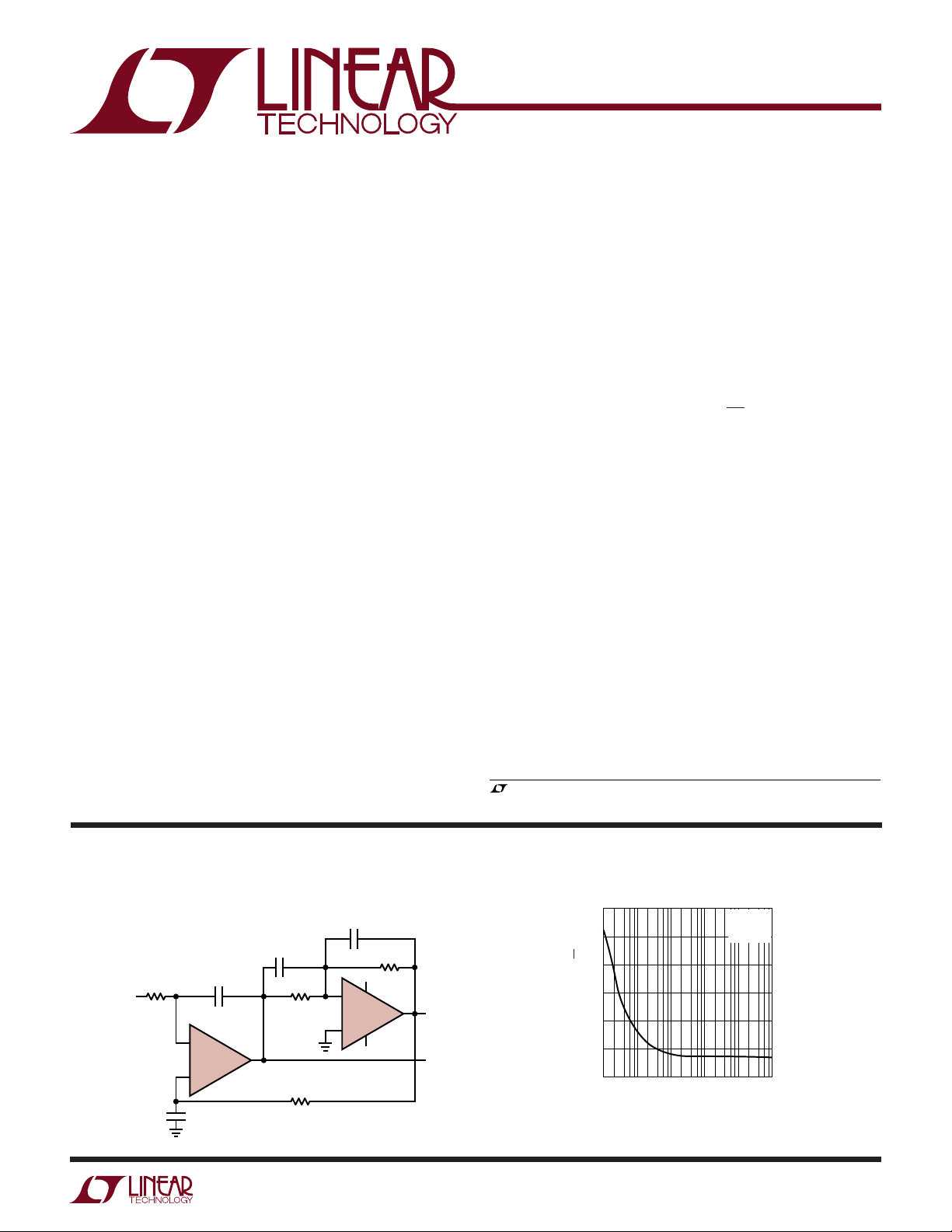
TYPICAL APPLICATIO
Low Noise Single-Ended Input to Differential Output Amplifi er
C3
10pF
C4
10pF
–
LTC6241
+
10pF
1/2
C1
R3
4.99k
R2
200k
R1
200k
V
IN
C2
10pF
+2.5V
–
LTC6241
+
–2.5V
R4
4.99k
1/2
6241 TA01a
Noise Voltage vs Frequency
60
50
40
30
+
V
OUT
V
OUT
20
NOISE VOLTAGE (nV/√Hz)
10
0
10
1 100 1k 100k
FREQUENCY (Hz)
TA = 25°C
= ±2.5V
V
S
= 0V
V
CM
10k
6241 TA01b
624012fc
1
Page 2
LTC6240/LTC6241/LTC6242
WW
W
ABSOLUTE AXI U RATI GS
U
(Note 1)
Total Supply Voltage (V+ to V–)
LTC6240/LTC6241/LTC6242 ...................................7V
LTC6240HV/LTC6241HV/LTC6242HV ...................12V
+
Input Voltage .......................... (V
+ 0.3V) to (V– – 0.3V)
Input Current ........................................................±10mA
Output Short Circuit Duration (Note 2) ............ Indefi nite
Operating Temperature Range
LTC6240C/LTC6241C/LTC6242C .......... –40°C to 85°C
LTC6240I/LTC6241I/LTC6242I .............–40°C to 85°C
LTC6240H/LTC6241H/LTC6242H .......–40°C to 125°C
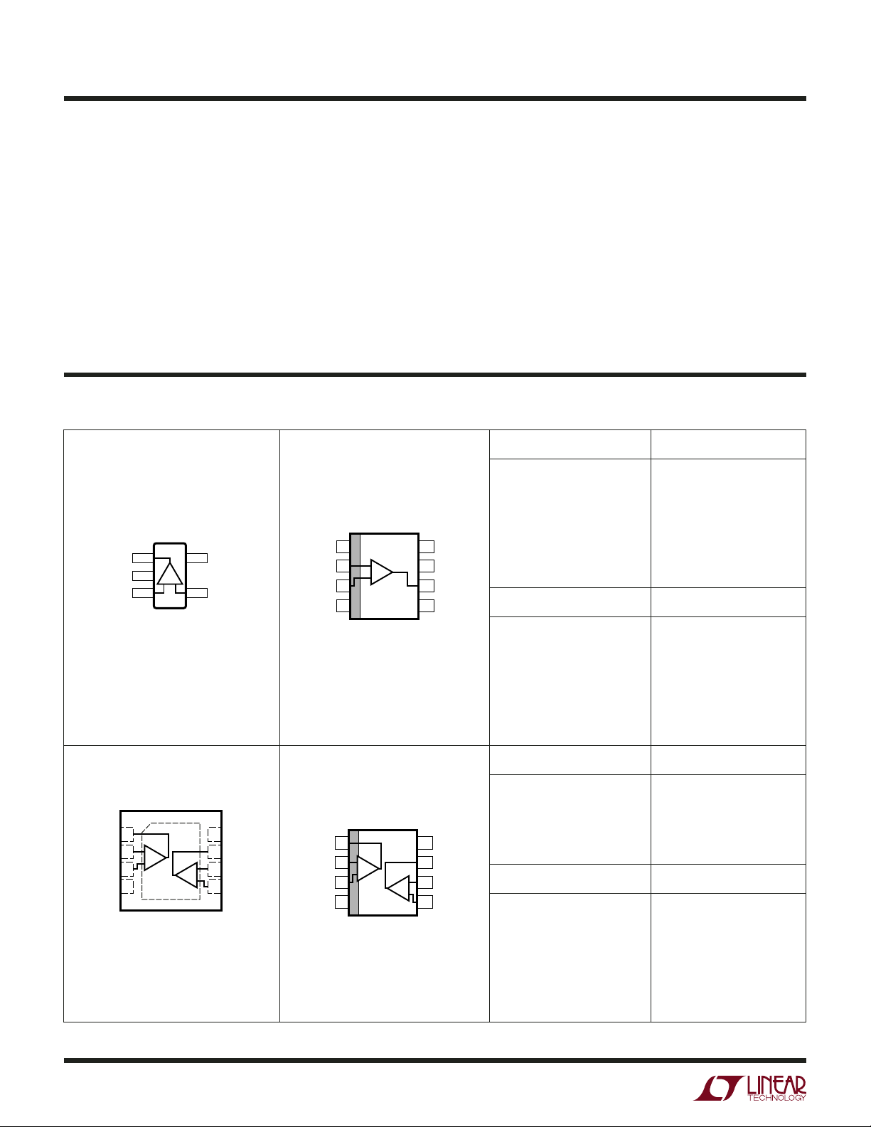
UUW
PACKAGE/ORDER I FOR ATIO
TOP VIEW
OUT 1
–
V
2
+
+IN 3
5-LEAD PLASTIC TSOT-23
T
= 150°C, θJA = 250°C/W
JMAX
–
S5 PACKAGE
5 V
4 –IN
+
NC
–IN
+IN
V
TOP VIEW
1
–
2
+
3
–
4
S8 PACKAGE
8-LEAD PLASTIC SO
T
= 150°C, θJA = 190°C/W
JMAX
Specifi ed Temperature Range (Note 3)
LTC6240C/LTC6241C/LTC6242C .............. 0°C to 70°C
LTC6240I/LTC6241I/LTC6242I .............–40°C to 85°C
LTC6240H/LTC6241H/LTC6242H .......–40°C to 125°C
Junction Temperature ........................................... 150°C
DHC, DD Package ............................................. 125°C
Storage Temperature Range ....................–65ºC to 150°C
DHC, DD Package ...............................–65ºC to 125°C
Lead Temperature (Soldering, 10 sec) .................. 300°C
ORDER PART NUMBER S5 PART MARKING*
LTC6240CS5
LTC6240HVCS5
LTC6240IS5
8
NC
+
V
7
OUT
6
NC
5
LTC6240HVIS5
LTC6240HS5
LTC6240HVHS5
ORDER PART NUMBER S8 PART MARKING
LTC6240CS8
LTC6240HVCS8
LTC6240IS8
LTC6240HVIS8
LTC6240HS8
LTC6240HVHS8
LTCRR
LTCRS
LTCRR
LTCRS
LTCRR
LTCRS
6240
6240HV
6240I
240HVI
6240H
240HVH
TOP VIEW
1OUT A
–IN A
2
+IN A
V
8-LEAD (3mm × 3mm) PLASTIC DFN
UNDERSIDE METAL CONNECTED TO V
A
3
–
4
DD PACKAGE
T
= 125°C, θJA = 43°C/W
JMAX
(PCB CONNECTION OPTIONAL)
2
ORDER PART NUMBER DD PART MARKING*
LTC6241CDD
+
8
V
OUT B
7
–IN B
6
B
+IN B
5
–
OUT A
–IN A
+IN A
V
TOP VIEW
1
2
A
3
–
4
S8 PACKAGE
8-LEAD PLASTIC SO
T
= 150°C, θJA = 190°C/W
JMAX
+
8
V
OUT B
7
–IN B
6
B
+IN B
5
LTC6241HVCDD
LTC6241IDD
LTC6241HVIDD
ORDER PART NUMBER S8 PART MARKING
LTC6241CS8
LTC6241HVCS8
LTC6241IS8
LTC6241HVIS8
LTC6241HS8
LTC6241HVHS8
LBPD
LBRR
LBPD
LBRR
6241
6241HV
6241I
241HVI
6241H
241HVH
624012fc
Page 3
UUW
PACKAGE/ORDER I FOR ATIO
LTC6240/LTC6241/LTC6242
TOP VIEW
OUT A
1
–IN A
2
+IN A
V
+IN B
–IN B
OUT B
NC
16-LEAD (5mm × 3mm) PLASTIC DFN
UNDERSIDE METAL CONNECTED TO V
A
3
+
4
5
B
6
7
8
DHC16 PACKAGE
T
= 125°C, θJA = 43°C/W
JMAX
(PCB CONNECTION OPTIONAL)
16
OUT D
15
–IN D
D
14
+IN D
–
13
17
V
+IN C
12
C
–IN C
11
OUT C
10
NC
9
TOP VIEW
1
OUT A
2
–IN A
+IN A
V
+IN B
–IN B
OUT B
NC
–
A
3
+
4
5
B
6
7
8
GN PACKAGE
16-LEAD PLASTIC SSOP
T
= 150°C, θJA = 135°C/W
JMAX
OUT D
16
–IN D
15
D
+IN D
14
–
V
13
+IN C
12
C
–IN C
11
OUT C
10
NC
9
ORDER PART NUMBER DHC PART MARKING*
LTC6242CDHC
LTC6242HVCDHC
LTC6242IDHC
LTC6242HVIDHC
6242
6242HV
6242
6242HV
ORDER PART NUMBER GN PART MARKING
LTC6242CGN
LTC6242HVCGN
LTC6242IGN
LTC6242HVIGN
LTC6242HGN
LTC6242HVHGN
6242
6242HV
6242I
242HVI
6242H
242HVH
Order Options Tape and Reel: Add #TR Lead Free: Add #PBF Lead Free Tape and Reel: Add #TRPBF
Lead Free Part Marking: http://www.linear.com/leadfree/
*The temperature grade is identifi ed by a label on the shipping container. Consult LTC Marketing for parts specifi ed with wider operating temperature ranges.
U
AVAILABLE OPTIO S
PART NUMBER AMPS/PACKAGE SPECIFIED TEMP RANGE SPECIFIED SUPPLY VOLTAGE PACKAGE PART MARKING
LTC6240CS5 1 0°C to 70°C 3V, 5V SOT-23 LTCRR
LTC6240CS8 1 0°C to 70°C 3V, 5V SO-8 6240
LTC6240HVCS5 1 0°C to 70°C 3V, 5V, ±5V SOT-23 LTCRS
LTC6240HVCS8 1 0°C to 70°C 3V, 5V, ±5V SO-8 6240HV
LTC6240IS5 1 –40°C to 85°C 3V, 5V SOT-23 LTCRR
LTC6240IS8 1 –40°C to 85°C 3V, 5V SO-8 6240I
LTC6240HVIS5 1 –40°C to 85°C 3V, 5V, ±5V SOT-23 LTCRS
LTC6240HVIS8 1 –40°C to 85°C 3V, 5V, ±5V SO-8 240HVI
LTC6240HS5 1 –40°C to 125°C 3V, 5V SOT-23 LTCRR
LTC6240HS8 1 –40°C to 125°C 3V, 5V SO-8 6240H
LTC6240HVHS5 1 –40°C to 125°C 3V, 5V, ±5V SOT-23 LTCRS
LTC6240HVHS8 1 –40°C to 125°C 3V, 5V, ±5V SO-8 240HVH
LTC6241CS8 2 0°C to 70°C 3V, 5V SO-8 6241
LTC6241CDD 2 0°C to 70°C 3V, 5V DD LBPD
LTC6241HVCS8 2 0°C to 70°C 3V, 5V, ±5V SO-8 6241HV
LTC6241HVCDD 2 0°C to 70°C 3V, 5V, ±5V DD LBRR
LTC6241IS8 2 –40°C to 85°C 3V, 5V SO-8 6241I
LTC6241IDD 2 –40°C to 85°C 3V, 5V DD LBPD
LTC6241HVIS8 2 –40°C to 85°C 3V, 5V, ±5V SO-8 241HVI
LTC6241HVIDD 2 –40°C to 85°C 3V, 5V, ±5V DD LBRR
LTC6241HS8 2 –40°C to 125°C 3V, 5V SO-8 6241H
LTC6241HVHS8 2 –40°C to 125°C 3V, 5V, ±5V SO-8 241HVH
624012fc
3
Page 4
LTC6240/LTC6241/LTC6242
U
AVAILABLE OPTIO S
PART NUMBER AMPS/PACKAGE SPECIFIED TEMP RANGE SPECIFIED SUPPLY VOLTAGE PACKAGE PART MARKING
LTC6242CGN 4 0°C to 70°C 3V, 5V GN 6242
LTC6242CDHC 4 0°C to 70°C 3V, 5V DHC 6242
LTC6242HVCGN 4 0°C to 70°C 3V, 5V, ±5V GN 6242HV
LTC6242HVCDHC 4 0°C to 70°C 3V, 5V, ±5V DHC 6242HV
LTC6242IGN 4 –40°C to 85°C 3V, 5V GN 6242I
LTC6242IDHC 4 –40°C to 85°C 3V, 5V DHC 6242
LTC6242HVIGN 4 –40°C to 85°C 3V, 5V, ±5V GN 242HVI
LTC6242HVIDHC 4 –40°C to 85°C 3V, 5V, ±5V DHC 6242HV
LTC6242HGN 4 –40°C to 125°C 3V, 5V GN 6242H
LTC6242HVHGN 4 –40°C to 125°C 3V, 5V, ±5V GN 242HVH
(LTC6240C/I, LTC6240HVC/I, LTC6241C/I, LTC6241HVC/I, LTC6242C/I,
ELECTRICAL CHARACTERISTICS
LTC6242HVC/I) The ● denotes the specifi cations which apply over the specifi ed temperature range, otherwise specifi cations are at
TA = 25°C. VS = 5V, 0V, VCM = 2.5V unless otherwise noted.
SYMBOL PARAMETER CONDITIONS MIN TYP MAX UNITS
V
OS
TC V
I
B
I
OS
OS
Input Offset Voltage (Note 4) LTC6241 S8
V
Match Channel-to-Channel (Note 5) LTC6241 S8
OS
Input Offset Voltage Drift (Note 6)
Input Bias Current (Notes 4, 7) LTC6241, LTC6242
Input Offset Current (Notes 4, 7) LTC6241, LTC6242
Input Noise Voltage 0.1Hz to 10Hz 550 nV
0°C to 70°C
–40°C to 85°C
LTC6242 GN
0°C to 70°C
–40°C to 85°C
LTC6240
0°C to 70°C
–40°C to 85°C
LTC6241 DD, LTC6242 DHC
0°C to 70°C
–40°C to 85°C
0°C to 70°C
–40°C to 85°C
LTC6242 GN
0°C to 70°C
–40°C to 85°C
LTC6241 DD, LTC6242 DHC
0°C to 70°C
–40°C to 85°C
LTC6240
LTC6240
●
●
●
●
●
●
●
●
●
●
●
●
●
●
●
●
●
●
●
40 125
250
300
50 150
275
300
50 175
300
350
100 550
650
725
40 160
300
375
50 185
325
400
150 650
700
750
0.7 2.5 µV/°C
0.2
75
0.2 1
75
0.2
75
0.2 1
75
µV
µV
µV
µV
µV
µV
µV
µV
µV
µV
µV
µV
µV
µV
µV
µV
µV
µV
µV
µV
µV
pA
pA
pA
pA
pA
pA
pA
pA
P-P
4
624012fc
Page 5
LTC6240/LTC6241/LTC6242
(LTC6240C/I, LTC6240HVC/I, LTC6241C/I, LTC6241HVC/I, LTC6242C/I,
ELECTRICAL CHARACTERISTICS
LTC6242HVC/I) The ● denotes the specifi cations which apply over the specifi ed temperature range, otherwise specifi cations are at
T
= 25°C. VS = 5V, 0V, VCM = 2.5V unless otherwise noted.
A
SYMBOL PARAMETER CONDITIONS MIN TYP MAX UNITS
e
n
i
n
R
IN
C
IN
V
CM
CMRR Common Mode Rejection 0V ≤ V
A
VOL
V
OL
V
OH
PSRR Power Supply Rejection V
I
SC
I
S
GBW Gain Bandwidth Product Frequency = 20kHz, R
SR Slew Rate (Note 11) A
FPBW Full Power Bandwidth (Note 12) V
t
s
Input Noise Voltage Density f = 1kHz 7 10 nV/√Hz
Input Noise Current Density (Note 8) 0.56 fA/√Hz
3.5
12
pF
3
pF
Input Resistance Common Mode 10
Input Capacitance
f = 100kHz
Differential Mode
Common Mode
Input Voltage Range Guaranteed by CMRR
≤ 3.5V
CM
●
0 3.5 V
●
80 105 dB
CMRR Match
Channel-to-Channel (Note 5)
●
76 95 dB
Large Signal Voltage Gain VO = 1V to 4V
R
= 10k to VS/2
L
0°C to 70°C
–40°C to 85°C
425
●
300
●
200
1600 V/mV
V/mV
V/mV
VO = 1.5V to 3.5V
R
= 1k to VS/2
L
0°C to 70°C
–40°C to 85°C
Output Voltage Swing Low (Note 9) No Load
I
= 1mA
SINK
I
= 5mA
SINK
Output Voltage Swing High (Note 9) No Load
I
SOURCE
I
SOURCE
= 2.8V to 6V, VCM = 0.2V
S
= 1mA
= 5mA
90
●
60
●
50
●
●
●
●
●
●
●
80 104 dB
215 V/mV
7
40
190
11
45
190
30
75
325
30
75
325
V/mV
V/mV
mV
mV
mV
mV
mV
mV
PSRR Match
Channel-to-Channel (Note 5)
Minimum Supply Voltage (Note 10)
Short-Circuit Current
Supply Current per Amplifi er LTC6241, LTC6242
0°C to 70°C
–40°C to 85°C
LTC6240
0°C to 70°C
–40°C to 85°C
= –2, RL = 1kΩ
V
= 3V
, RL = 1kΩ
P-P
= 2V, AV = –1, RL = 1kΩ, 0.1% 1100 ns
Settling Time V
OUT
STEP
= 1kΩ
L
●
74 100 dB
●
2.8 V
●
15 30 mA
1.8 2.2
●
●
2.3
2.4
22.4
●
●
●
13 18 MHz
●
5 10 V/µs
●
0.53 1.06 MHz
2.5
2.6
mA
mA
mA
mA
mA
mA
Ω
624012fc
5
Page 6
LTC6240/LTC6241/LTC6242
(LTC6240C/I, LTC6240HVC/I, LTC6241C/I, LTC6241HVC/I, LTC6242C/I,
ELECTRICAL CHARACTERISTICS
LTC6242HVC/I) The ● denotes the specifi cations which apply over the specifi ed temperature range, otherwise specifi cations are at
TA = 25°C. VS = 3V, 0V, VCM = 1.5V unless otherwise noted.
SYMBOL PARAMETER CONDITIONS MIN TYP MAX UNITS
V
OS
TC V
OS
I
B
I
OS
V
CM
CMRR Common Mode Rejection 0V ≤ V
A
VOL
V
OL
V
OH
PSRR Power Supply Rejection VS = 2.8V to 6V, VCM = 0.2V
I
SC
I
S
GBW Gain Bandwidth Product Frequency = 20kHz, R
Input Offset Voltage (Note 4) LTC6241 S8
0°C to 70°C
–40°C to 85°C
LTC6242 GN
0°C to 70°C
–40°C to 85°C
LTC6240
0°C to 70°C
–40°C to 85°C
LTC6241 DD, LTC6242 DHC
0°C to 70°C
–40°C to 85°C
Match Channel-to-Channel (Note 5) LTC6241 S8
V
OS
0°C to 70°C
–40°C to 85°C
LTC6242 GN
0°C to 70°C
–40°C to 85°C
LTC6241 DD, LTC6242 DHC
0°C to 70°C
–40°C to 85°C
Input Offset Voltage Drift (Note 6)
Input Bias Current (Notes 4, 7) LTC6241, LTC6242
LTC6240
Input Offset Current (Notes 4, 7) LTC6241, LTC6242
LTC6240
Input Voltage Range Guaranteed by CMRR
≤ 1.5V
CM
CMRR Match
Channel-to-Channel (Note 5)
Large Signal Voltage Gain VO = 1V to 2V
= 10k to VS/2
R
L
0°C to 70°C
–40°C to 85°C
Output Voltage Swing Low (Note 9) No Load
= 1mA
I
SINK
Output Voltage Swing High (Note 9) No Load
= 1mA
I
SOURCE
PSRR Match
Channel-to-Channel (Note 5)
Minimum Supply Voltage (Note 10)
Short-Circuit Current
Supply Current per Amplifi er LTC6241, LTC6242
0°C to 70°C
–40°C to 85°C
LTC6240
0°C to 70°C
–40°C to 85°C
= 1kΩ
L
●
●
275
325
60 200
40 175
●
●
275
325
50 200
●
●
325
375
100 550
●
●
650
725
40 200
●
●
325
400
60 225
●
●
325
400
150 650
●
●
●
0.7 2.5 µV/°C
700
750
0.2
●
75
0.2 1
●
75
0.2
●
75
0.2 1
●
●
0 1.5 V
●
78 100 dB
●
76 95 dB
140
●
100
●
75
●
●
●
●
●
80 104 dB
●
74 100 dB
●
2.8 V
●
36 mA
600 V/mV
3
65
4
70
75
30
110
30
120
1.4 1.7
●
●
1.8
1.9
1.5 1.9
●
●
●
12 17 MHz
2
2.1
µV
µV
µV
µV
µV
µV
µV
µV
µV
µV
µV
µV
µV
µV
µV
µV
µV
µV
µV
µV
µV
pA
pA
pA
pA
pA
pA
pA
pA
V/mV
V/mV
mV
mV
mV
mV
mA
mA
mA
mA
mA
mA
624012fc
6
Page 7

LTC6240/LTC6241/LTC6242
(LTC6240HVC/I, LTC6241HVC/I, LTC6242HVC/I) The ● denotes the
ELECTRICAL CHARACTERISTICS
specifi cations which apply over the specifi ed temperature range, otherwise specifi cations are at TA = 25°C. VS = ±5V, 0V, VCM = 0V
unless otherwise noted.
SYMBOL PARAMETER CONDITIONS MIN TYP MAX UNITS
V
OS
Input Offset Voltage (Note 4) LTC6241 S8
0°C to 70°C
–40°C to 85°C
LTC6242 GN
0°C to 70°C
–40°C to 85°C
LTC6240
0°C to 70°C
–40°C to 85°C
LTC6241 DD, LTC6242 DHC
0°C to 70°C
–40°C to 85°C
Match Channel-to-Channel (Note 5) LTC6241 S8
V
OS
0°C to 70°C
–40°C to 85°C
LTC6242 GN
0°C to 70°C
–40°C to 85°C
LTC6241 DD, LTC6242 DHC
0°C to 70°C
–40°C to 85°C
TC V
I
B
OS
Input Offset Voltage Drift (Note 6)
Input Bias Current (Notes 4, 7) LTC6241, LTC6242
LTC6240
I
OS
Input Offset Current (Notes 4, 7) LTC6241, LTC6242
LTC6240
Input Noise Voltage 0.1Hz to 10Hz 550 nV
e
n
i
n
R
IN
C
IN
Input Noise Voltage Density f = 1kHz 7 10 nV/√Hz
Input Noise Current Density (Note 8) 0.56 fA/√Hz
Input Resistance Common Mode 10
Input Capacitance
f = 100kHz
Differential Mode
Common Mode
V
CM
Input Voltage Range Guaranteed by CMRR
CMRR Common Mode Rejection –5V ≤ V
CMRR Match
Channel-to-Channel (Note 5)
A
VOL
Large Signal Voltage Gain VO = –3.5V to 3.5V
= 10k
R
L
0°C to 70°C
–40°C to 85°C
= 1k
R
L
0°C to 70°C
–40°C to 85°C
V
OL
Output Voltage Swing Low (Note 9) No Load
= 1mA
I
SINK
= 10mA
I
SINK
CM
≤ 3.5V
●
●
60 200
50 175
●
●
60 250
●
●
100 550
●
●
50 200
●
●
60 225
●
●
150 650
●
●
●
0.7 2.5 µV/°C
0.5
●
0.5 1
●
0.2
●
0.2 1
●
12
3.5
3
●
–5 3.5 V
●
83 105 dB
76 95 dB
●
775
●
600
●
500
150
●
90
●
75
●
●
●
2700 V/mV
360 V/mV
15
45
360
275
325
275
325
350
400
650
725
325
400
325
400
700
750
75
75
75
75
30
75
550
µV
µV
µV
µV
µV
µV
µV
µV
µV
µV
µV
µV
µV
µV
µV
µV
µV
µV
µV
µV
µV
pA
pA
pA
pA
pA
pA
pA
pA
P-P
pF
pF
V/mV
V/mV
V/mV
V/mV
mV
mV
mV
Ω
624012fc
7
Page 8
LTC6240/LTC6241/LTC6242
(LTC6240HVC/I, LTC6241HVC/I, LTC6242HVC/I) The ● denotes the
ELECTRICAL CHARACTERISTICS
specifi cations which apply over the specifi ed temperature range, otherwise specifi cations are at TA = 25°C. VS = ±5V, 0V, VCM = 0V
unless otherwise noted.
SYMBOL PARAMETER CONDITIONS MIN TYP MAX UNITS
V
OH
PSRR Power Supply Rejection V
Output Voltage Swing High (Note 9) No Load
I
SOURCE
I
SOURCE
= 2.8V to 11V, VCM = 0.2V
S
= 1mA
= 10mA
PSRR Match
Channel-to-Channel (Note 5)
Minimum Supply Voltage (Note 10)
I
SC
I
S
Short-Circuit Current
Supply Current per Amplifi er LTC6241, LTC6242
0°C to 70°C
–40°C to 85°C
LTC6240
0°C to 70°C
–40°C to 85°C
GBW Gain Bandwidth Product Frequency = 20kHz, R
SR Slew Rate (Note 11) A
FPBW Full Power Bandwidth (Note 12) V
t
s
Settling Time V
= –2, RL = 1kΩ
V
= 3V
OUT
STEP
, RL = 1kΩ
P-P
= 2V, AV = –1, RL = 1kΩ, 0.1% 900 ns
= 1kΩ
L
●
●
●
●
85 110 dB
●
82 106 dB
●
2.8 V
●
15 35 mA
15
45
360
30
75
550
2.5 3.2
●
●
3.3
3.7
2.7 3.3
●
●
●
13 18 MHz
●
5.5 10 V/µs
●
0.58 1.06 MHz
3.4
3.8
mV
mV
mV
mA
mA
mA
mA
mA
mA
(LTC6240H/LTC6240HVH, LTC6241H/LTC6241HVH, LTC6242H/LTC6242HVH) The ● denotes the specifi cations which apply from –40°C
to 125°C, otherwise specifi cations are at TA = 25°C. VS = 5V, 0V, VCM = 2.5V unless otherwise noted.
SYMBOL PARAMETER CONDITIONS MIN TYP MAX UNITS
V
OS
TC V
OS
I
B
I
OS
V
CM
CMRR Common Mode Rejection 0V ≤ V
A
VOL
Input Offset Voltage (Note 4) LTC6241 S8
LTC6242 GN
LTC6240
Match Channel-to-Channel (Note 5) LTC6241 S8
V
OS
LTC6242 GN
Input Offset Voltage Drift (Note 6)
Input Bias Current (Notes 4, 7) LTC6241, LTC6242
LTC6240
Input Offset Current (Notes 4, 7) LTC6241, LTC6242
LTC6240
Input Voltage Range Guaranteed by CMRR
≤ 3.5V
CM
CMRR Match
Channel-to-Channel (Note 5)
Large Signal Voltage Gain VO = 1V to 4V
= 10k to VS/2
R
L
= 1.5V to 3.5V
V
O
= 1k to VS/2
R
L
●
50 150
40 125
●
50 175
●
40 160
●
50 185
●
●
0.7 2.5 µV/°C
0.2
●
0.2 1
●
0.2
●
0.2 1
●
●
0 3.5 V
●
78 dB
●
74 dB
425
●
200
90
●
40
1600 V/mV
215 V/mV
400
400
450
400
400
1.5
2.5
150
750
µV
µV
µV
µV
µV
µV
µV
µV
µV
µV
pA
nA
pA
nA
pA
pA
pA
pA
V/mV
V/mV
624012fc
8
Page 9
LTC6240/LTC6241/LTC6242
(LTC6240H/LTC6240HVH, LTC6241H/LTC6241HVH, LTC6242H/LTC6242HVH)
ELECTRICAL CHARACTERISTICS
The
● denotes the specifi cations which apply from –40°C to 125°C, otherwise specifi cations are at T
unless otherwise noted.
SYMBOL PARAMETER CONDITIONS MIN TYP MAX UNITS
V
OL
V
OH
PSRR Power Supply Rejection V
I
SC
I
S
GBW Gain Bandwidth Product Frequency = 20kHz, R
SR Slew Rate (Note 11) A
FPBW Full Power Bandwidth (Note 12) V
Output Voltage Swing Low (Note 9) No Load
= 1mA
I
SINK
= 5mA
I
SINK
Output Voltage Swing High (Note 9) No Load
= 1mA
I
SOURCE
I
= 5mA
SOURCE
= 2.8V to 6V, VCM = 0.2V
S
PSRR Match
Channel-to-Channel (Note 5)
Minimum Supply Voltage (Note 10)
Short-Circuit Current
Supply Current per Amplifi er LTC6241, LTC6242
LTC6240
= –2, RL = 1kΩ
V
= 3V
OUT
, RL = 1kΩ
P-P
= 1kΩ
L
= 25°C. VS = 5V, 0V, VCM = 2.5V
A
●
●
●
●
●
●
●
78 dB
●
74 dB
●
2.8 V
●
15 mA
30
85
325
30
85
325
1.8 2.2
●
2.4
2 2.4
●
●
12 MHz
●
4.5 V/µs
●
0.48 MHz
2.8
mV
mV
mV
mV
mV
mV
mA
mA
mA
mA
(LTC6240H/LTC6240HVH, LTC6241H/LTC6241HVH, LTC6242H/LTC6242HVH) The ● denotes the specifi cations which apply from –40°C
to 125°C, otherwise specifi cations are at TA = 25°C. VS = 3V, 0V, VCM = 1.5V unless otherwise noted.
SYMBOL PARAMETER CONDITIONS MIN TYP MAX UNITS
V
OS
Input Offset Voltage (Note 4) LTC6241 S8
LTC6242 GN
LTC6240
VOS Match Channel-to-Channel (Note 5) LTC6241 S8
LTC6242 GN
TC V
I
B
OS
Input Offset Voltage Drift (Note 6)
Input Bias Current (Notes 4, 7) LTC6241, LTC6242
LTC6240
I
OS
Input Offset Current (Notes 4, 7) LTC6241, LTC6242
LTC6240
V
CM
Input Voltage Range Guaranteed by CMRR
CMRR Common Mode Rejection 0V ≤ V
CMRR Match
Channel-to-Channel (Note 5)
A
VOL
Large Signal Voltage Gain VO = 1V to 2V
R
= 10k to VS/2
L
CM
≤ 1.5V
●
●
●
●
●
●
●
●
●
●
●
0 1.5 V
●
75 dB
●
74 dB
140
●
65
40 175
400
60 200
400
50 200
450
40 200
400
60 225
400
µV
µV
µV
µV
µV
µV
µV
µV
µV
µV
0.7 2.5 µV/°C
0.2
1.5
0.2 1
2.5
0.2
150
0.2 1
750
pA
nA
pA
nA
pA
pA
pA
pA
600 V/mV
V/mV
624012fc
9
Page 10

LTC6240/LTC6241/LTC6242
(LTC6240H/LTC6240HVH, LTC6241H/LTC6241HVH, LTC6242H/LTC6242HVH)
ELECTRICAL CHARACTERISTICS
The ● denotes the specifi cations which apply from –40°C to 125°C, otherwise specifi cations are at TA = 25°C. VS = 3V, 0V, VCM = 1.5V
unless otherwise noted.
SYMBOL PARAMETER CONDITIONS MIN TYP MAX UNITS
V
OL
V
OH
Output Voltage Swing Low (Note 9) No Load
I
= 1mA
SINK
Output Voltage Swing High (Note 9) No Load
I
SOURCE
= 1mA
PSRR Power Supply Rejection VS = 2.8V to 6V, VCM = 0.2V
PSRR Match Channel-to-Channel
(Note 5)
Minimum Supply Voltage (Note 10)
I
SC
I
S
Short-Circuit Current
Supply Current per Amplifi er LTC6241, LTC6242
LTC6240
GBW Gain Bandwidth Product Frequency = 20kHz, RL = 1kΩ
(LTC6240HVH/LTC6241HVH/LTC6242HVH) The ● denotes the specifi cations which apply from –40°C to 125°C, otherwise specifi cations
are at TA = 25°C. VS = ±5V, VCM = 0V unless otherwise noted.
SYMBOL PARAMETER CONDITIONS MIN TYP MAX UNITS
V
OS
TC V
OS
I
B
I
OS
V
CM
CMRR Common Mode Rejection –5V ≤ V
A
VOL
Input Offset Voltage (Note 4) LTC6241 S8
LTC6242 GN
LTC6240
Match Channel-to-Channel (Note 5) LTC6241 S8
V
OS
LTC6242 GN
Input Offset Voltage Drift (Note 6)
Input Bias Current (Notes 4, 7) LTC6241, LTC6242
LTC6240
Input Offset Current (Notes 4, 7) LTC6241, LTC6242
LTC6240
Input Voltage Range Guaranteed by CMRR
≤ 3.5V
CM
CMRR Match
Channel-to-Channel (Note 5)
Large Signal Voltage Gain VO = –3.5V to 3.5V
R
= 10k
L
R
= 1k
L
●
●
●
●
●
78 dB
●
74 dB
●
2.8 V
●
2.5 mA
1.4 1.7
●
1.5 1.9
●
●
10 MHz
50 175
●
60 200
●
60 250
●
50 200
●
60 225
●
●
0.7 2.5 µV/°C
0.5
●
0.5 1
●
0.2
●
0.2 1
●
●
–5 3.5 V
●
80 dB
●
76 dB
775
●
350
150
●
60
2700 V/mV
360 V/mV
30
130
30
130
1.9
2.1
400
400
450
400
400
1.5
2.5
150
750
mV
mV
mV
mV
mA
mA
mA
mA
µV
µV
µV
µV
µV
µV
µV
µV
µV
µV
pA
nA
pA
nA
pA
pA
pA
pA
V/mV
V/mV
624012fc
10
Page 11

LTC6240/LTC6241/LTC6242
(LTC6240HVH/LTC6241HVH/LTC6242HVH) The ● denotes the specifi cations
ELECTRICAL CHARACTERISTICS
which apply from –40°C to 125°C, otherwise specifi cations are at T
SYMBOL PARAMETER CONDITIONS MIN TYP MAX UNITS
V
OL
V
OH
PSRR Power Supply Rejection V
I
SC
I
S
GBW Gain Bandwidth Product Frequency = 20kHz, RL = 1kΩ
SR Slew Rate (Note 11) A
FPBW Full Power Bandwidth (Note 12) V
Output Voltage Swing Low (Note 9) No Load
I
= 1mA
SINK
I
= 10mA
SINK
Output Voltage Swing High (Note 9) No Load
I
SOURCE
I
SOURCE
= 2.8V to 11V, VCM = 0.2V
S
PSRR Match
Channel-to-Channel (Note 5)
Minimum Supply Voltage (Note 10)
Short-Circuit Current
Supply Current per Amplifi er LTC6241, LTC6242
LTC6240
= –2, RL = 1kΩ
V
= 3V
OUT
= 25°C. VS = ±5V, VCM = 0V unless otherwise noted.
A
●
●
●
●
= 1mA
= 10mA
, RL = 1kΩ
P-P
●
●
●
83 dB
●
82 dB
●
2.8 V
●
15 mA
●
●
●
12 MHz
●
5 V/µs
●
0.53 MHz
30
85
600
30
85
600
2.5 3.2
3.7
2.7 3.3
3.8
mV
mV
mV
mV
mV
mV
mA
mA
mA
mA
Note 1: Stresses beyond those listed under Absolute Maximum Ratings
may cause permanent damage to the device. Exposure to any Absolute
Maximum Rating condition for extended periods may affect device
reliability and lifetime.
Note 2: A heat sink may be required to keep the junction temperature
below the absolute maximum rating when the output is shorted
indefi nitely.
Note 3: The LTC6240C/LTC6240HVC/LTC6241C/LTC6241HVC, LTC6242C/
LTC6242HVC are guaranteed to meet specifi ed performance from 0°C to
70°C. They are designed, characterized and expected to meet specifi ed
performance from –40°C to 85°C, but are not tested or QA sampled at
these temperatures. The LTC6240I/LTC6240HVI, LTC6241I/LTC6241HVI,
LTC6242I/LTC6242HVI are guaranteed to meet specifi ed performance
from –40°C to 85°C. All versions of the LTC6240H/LTC6241H/LTC6242H
are guaranteed to meet specifi ed performance
from –40°C to 125°C.
Note 4: ESD (Electrostatic Discharge) sensitive device. ESD protection
devices are used extensively internal to the LTC6240/LTC6241/LTC6242;
however, high electrostatic discharge can damage or degrade the device.
Use proper ESD handling precautions.
Note 5: Matching parameters are the difference between the two amplifi ers
A and D and between B and C of the LTC6242; between the two amplifi ers
of the LTC6241. CMRR and PSRR match are defi ned as follows: CMRR
and PSRR are measured in µV/V on the matched amplifi ers. The difference
is calculated between the matching sides in µV/V. The result is converted
to dB.
Note 6: This parameter is not 100% tested.
Note 7: Bias current at T
= 25°C is 100% tested and guaranteed for the
A
LTC6240 in the S8 package. The LTC6240S5, LTC6241 and LTC6242 are
expected to achieve the same performance as the LTC6240S8. All parts are
guaranteed to meet specifi cations over temperature.
Note 8: Current noise is calculated from the formula: i
where q = 1.6 × 10
–19
coulomb. The noise of source resistors up to
n
= (2qIB)
1/2
50GΩ dominates the contribution of current noise. See also Typical
Characteristics curve Noise Current vs Frequency.
Note 9: Output voltage swings are measured between the output and
power supply rails.
Note 10: Minimum supply voltage is guaranteed by the power supply
rejection ratio test.
Note 11: Slew rate is measured in a gain of –2 with R
500Ω. On the LTC6240/LTC6241/LTC6242, V
V
slew rate is measured between –1V and +1V. On the LTC6240HV/
OUT
LTC6241HV/LTC6242HV, V
is ±2V and V
IN
S
OUT
= 1k and RG =
F
= ±2.5V, VIN is ±1V and
slew rate is measured
between –2V and +2V.
Note 12: Full-power bandwidth is calculated from the slew rate:
FPBW = SR/πV
P-P
.
624012fc
11
Page 12

LTC6240/LTC6241/LTC6242
UW
TYPICAL PERFOR A CE CHARACTERISTICS
VOS Distribution LTC6241 VOS Distribution LTC6241
90
VS = ±2.5V
SO-8 PACKAGE
80
70
60
50
40
30
NUMBER OF UNITS
20
10
0
–70 –50 –30 –10 7030 5010
INPUT OFFSET VOLTAGE (µV)
35
VS = ±2.5V
30
25
20
15
PERCENT OF UNITS
10
5
0
–70–90–110 –50 –30 –10 7030 5010
INPUT OFFSET VOLTAGE (µV)
6241 G01
6241 G43
120
VS = ±2.5V
DD PACKAGE
100
80
60
40
NUMBER OF UNITS
20
0
–350 –250 –150 –50 350150 25050
INPUT OFFSET VOLTAGE (µV)
VOS Temperature Coeffi cient
Distribution LTC6240VOS Distribution LTC6240
18
16
14
12
10
8
6
NUMBER OF UNITS
4
2
0
–0.6 –0.2 1.81.41.00.60.2
DISTRIBUTION (µV/°C)
VS = 5V, 0
= 2.5V
V
CM
2 LOTS
–40°C TO 125°C
SO-8 AND SOT23
PACKAGES
6241 G02
6241 G44
V
Temperature Coeffi cient
OS
Distribution LTC6241
16
VS = ±2.5V
2 LOTS
14
–55°C TO 125°C
12
10
8
6
NUMBER OF UNITS
4
2
0
–1.0 –0.6 –0.2 0.2 1.81.0 1.40.6
DISTRIBUTION (µV/°C)
Supply Current vs Supply Voltage
3.5
3.0
2.5
2.0
1.5
1.0
SUPPLY CURRENT PER AMP (mA)
0.5
0
0
24
TOTAL SUPPLY VOLTAGE (V)
TA = 25°C
TA = –55°C
TA = 125°C
812
610
6241 G03
6241 G04
Offset Voltage vs Input Common
Mode Voltage
300
250
200
150
100
50
0
–50
–100
OFFSET VOLTAGE (µV)
–150
–200
–250
–300
0 0.5 1.5 2.5 3.5
–0.5
INPUT COMMON MODE VOLTAGE (V)
1.0
TA = 125°C
TA = 25°C
TA = –55°C
2.0
12
VS = 5V, 0V
3.0
6241 G05
Input Bias Current vs Common
Mode Voltage
1000
VS = 5V, 0V
TA = 125°C
100
10
TA = 85°C
1
INPUT BIAS CURRENT (pA)
TA = 25°C
4.54.0
0.1
0 1.0 2.0 3.0 4.00.5 1.5 2.5 3.5 4.5 5.0
COMMON MODE VOLTAGE (V)
6241 G06
Input Bias Current vs
Common Mode Voltage
700
VS = 5V, 0V
600
500
400
300
TA = 25°C
200
100
0
–100
INPUT BIAS CURRENT (pA)
–200
–300
–400
TA = 85°C
–0.8 –0.6 –0.2 0.2 0.6–0.4 0 0.4 0.8 1.0
COMMON MODE VOLTAGE (V)
TA = 125°C
6241 G07
624012fc
Page 13

LTC6240/LTC6241/LTC6242
UW
TYPICAL PERFOR A CE CHARACTERISTICS
Input Bias Current vs Temperature
1000
VCM = VS/2
100
10
1
INPUT BIAS CURRENT (pA)
0.1
25 45 65 85 10535 55 75 95 115 125
VS = 10V
VS = 5V
TEMPERATURE (°C)
Gain Bandwidth and Phase
Margin vs Temperature
±5V
±1.5V
CL = 5pF
R
L
V
=
S
PHASE MARGIN
40
30
V
=
±5V
S
20
GAIN BANDWIDTH (MHz)
V
=
±1.5V
S
10
0
–55 –35 5 45 85–15 25 65 105 125
V
=
S
GAIN BANDWIDTH
TEMPERATURE (°C)
= 1k
6241 G12
6241 G08
70
60
PHASE MARGIN (DEG)
50
40
30
Output Saturation Voltage vs
Load Current (Output Low)
10
VS = 5V, 0V
TA = 25°C
1
TA = 125°C
0.1
0.01
OUTPUT LOW SATURATION VOLTAGE (V)
0.001
0.1 10 100
1
LOAD CURRENT (mA)
TA = –55°C
Open Loop Gain vs Frequency
80
PHASE
70
60
50
GAIN
40
30
GAIN (dB)
20
10
0
–10
–20
10k 100k 10M1M 100M
V
=
S
V
S
V
=
±1.5V
S
FREQUENCY (Hz)
±1.5V
=
±5V
CL = 5pF
= 1k
R
L
= VS/2
V
CM
V
=
S
6241 G09
±5V
6241 G13
120
100
80
60
PHASE (DEG)
40
20
0
–20
–40
–60
–80
Output Saturation Voltage vs
Load Current (Output High)
10
VS = 5V, 0V
TA = 25°C
1
TA = 125°C
TA = –55°C
0.1
OUTPUT HIGH SATURATION VOLTAGE (V)
0.01
0.1 10 100
1
LOAD CURRENT (mA)
Gain Bandwidth and Phase
Margin vs Supply Voltage
TA = 25°C
= 5pF
C
L
= 1k
R
L
PHASE MARGIN
30
20
GAIN BANDWIDTH (MHz)
10
0
0482 6 10 12
GAIN BANDWIDTH
TOTAL SUPPLY VOLTAGE (V)
6241 G10
6241 G14
70
60
PHASE MARGIN (DEG)
50
40
Slew Rate vs Temperature
20
AV = –2
= 1k, RG = 500Ω
R
F
18
CONDITIONS: SEE NOTE 12
16
14
12
V
=
±2.5V FALLING
S
10
SLEW RATE (V/µs)
8
V
=
±2.5V RISING
S
6
4
–55 –35 5 45 85–15 25 65 105 125
TEMPERATURE (°C)
V
=
±5V FALLING
S
V
=
S
±5V RISING
6241 G15
Output Impedance vs Frequency
10k
TA = 25°C
= ±2.5V
V
S
1k
100
10
1
OUTPUT IMPEDANCE (Ω)
0.10
0.01
10k 1M 10M
AV = 10
AV = 1
100k
FREQUENCY (Hz)
AV = 2
6241 G16
Common Mode Rejection Ratio vs
Frequency
100
90
80
70
60
50
40
30
20
10
COMMON MODE REJECTION (dB)
0
–10
10k 100k 10M1M 100M
FREQUENCY (Hz)
T
= 25
A
V
=
S
13
°C
±2.5V
6241 G17
624012fc
Page 14

LTC6240/LTC6241/LTC6242
UW
TYPICAL PERFOR A CE CHARACTERISTICS
Power Supply Rejection Ratio vs
Channel Separation vs Frequency
0
–10
–20
–30
–40
–50
–60
–70
–80
VOLTAGE GAIN (dB)
–90
–100
–110
–120
10k 100k 10M1M 100M
FREQUENCY (Hz)
T
A
V
S
A
V
= 25
=
= 1
°C
±2.5V
6241 G18
Frequency
90
80
70
60
50
40
30
20
NEGATIVE SUPPLY
10
POWER SUPPLY REJECTION RATIO (dB)
0
1k 100k 1M 100M
POSITIVE SUPPLY
10k 10M
FREQUENCY (Hz)
T
V
A
S
= 25
=
°C
±2.5V
6241 G19
Input Capacitance vs Frequency
16
14
12
10
8
6
4
INPUT CAPACITANCE (pF)
2
0
1k 100k 1M 100M
10k 10M
FREQUENCY (Hz)
V
S
C
CM
=
±1.5V
6241 G20
Minimum Supply Voltage
100
VCM = VS/2
80
60
40
20
0
–20
–40
TA = 125°C
–60
CHANGE IN OFFSET VOLTAGE (µV)
–80
–100
02 614 8375910
TOTAL SUPPLY VOLTAGE (V)
TA = 25°C
TA = –55°C
6241 G21
Open Loop Gain
120
100
80
60
40
INPUT VOLTAGE (µV)
20
0
–20
012 534
RL = 10k
RL = 1k
OUTPUT VOLTAGE (V)
TA = 25°C
= 5V, 0V
V
S
6241 G24
Output Short Circuit Current vs
Power Supply Voltage Open Loop Gain
50
40
SINKING
30
20
10
0
–10
–20
SOURCING
–30
–40
OUTPUT SHORT-CIRCUIT CURRENT (mA)
–50
1.5 2.5 4.52.0 3.53.0 4.0 5.0
POWER SUPPLY VOLTAGE (±V)
TA = –55°C
TA = 25°C
TA = –55°C
Open Loop Gain
100
80
60
40
20
0
INPUT VOLTAGE (µV)
–20
–40
–60
–5 –4 0–2–3 –1 51234
OUTPUT VOLTAGE (V)
RL = 10k
RL = 1k
TA = 125°C
TA = 125°C
6241 G22
TA = 25°C
= ±5V
V
S
6241 G25
120
100
80
60
40
INPUT VOLTAGE (µV)
20
0
0 0.5 2.51.51.0 2.0 3.0
Offset Voltage vs Output Current
500
400
300
200
100
0
–100
–200
OFFSET VOLTAGE (µV)
–300
–400
–500
–50 –40 –30 –20 –10 10 302004050
OUTPUT VOLTAGE (V)
TA = 125°C
TA = 25°C
TA = –55°C
OUTPUT CURRENT (mA)
RL = 100k
RL = 10k
TA = 25°C
= 3V, 0V
V
S
6241 G23
VS = ±5V
6241 G26
14
624012fc
Page 15

LTC6240/LTC6241/LTC6242
k
UW
TYPICAL PERFOR A CE CHARACTERISTICS
Warm-Up Drift vs Time
25
TA = 25°C
20
V
=
±5V
S
15
V
=
±2.5V
10
S
5
V
=
0
CHANGE IN OFFSET VOLTAGE (µV)
–5
010 3020540605015 3525 45 55
±1.5V
S
TIME AFTER POWER UP (s)
Noise Current vs Frequency
1000
T
= 25
°C
A
V
=
±2.5V
S
V
= 0V
CM
100
10
1
NOISE CURRENT (fA/√Hz)
0.1
100 10k 100
1k
FREQUENCY (Hz)
6241 G27
6241 G42
Noise Voltage vs Frequency
60
50
40
30
20
NOISE VOLTAGE (nV/√Hz)
10
0
10
1 100 1k 100k
FREQUENCY (Hz)
Series Output Resistance and
Overshoot vs Capacitive Load
60
50
40
30
OVERSHOOT (%)
20
10
0
75pF
1k
1k
R
–
+
10
S
C
L
R
= 10
Ω
S
100 1000
CAPACITIVE LOAD (pF)
TA = 25°C
= ±2.5V
V
S
= 0V
V
CM
10k
R
= 50
S
VS = ±2.5V
= –1
A
V
6241 G28
Ω
6241 G29
0.1Hz to 10Hz Voltage Noise
VS = 5V, 0V
VOLTAGE NOISE (200nV/DIV)
TIME (1s/DIV)
Minimum Output Series
Resistance vs Capacitive Load
1000
V
=
±2.5V
S
<30% OVERSHOOT
100
10
1
OUTPUT SERIES RESISTANCE (Ω)
0.1
10pF
0.01µF1µF0.1µF1000pF100pF
CAPACITIVE LOAD
6241 G11
10µF
6241 G45
Series Output Resistance and
Overshoot vs Capacitive Load
60
50
40
30
OVERSHOOT (%)
20
10
0
75pF
500
Ω
1k
R
–
+
10
S
C
L
R
= 10
S
100 1000
CAPACITIVE LOAD (pF)
Ω
R
= 50
S
VS = ±2.5V
= –2
A
V
6241 G30
Settling Time vs Output Step
(Non-Inverting)
3.5
TA = 25°C
= ±5V
V
S
3.0
= 1
A
V
2.5
V
IN
2.0
1.5
SETTLING TIME (µs)
Ω
1.0
0.5
1mV
10mV
0
–4 –2 3–3 10–1 2 4
OUTPUT STEP (V)
V
–
OUT
+
1k
1mV
10mV
6241 G31
Settling Time vs Output Step
(Inverting)
3.0
TA = 25°C
= ±5V
V
S
= –1
A
2.5
V
2.0
1.5
1.0
SETTLING TIME (µs)
0.5
0
–4 –2 3–3 10–1 2 4
V
IN
1mV
10mV
OUTPUT STEP (V)
1k
1k
–
+
V
OUT
1k
1mV
10mV
6241 G32
624012fc
15
Page 16

LTC6240/LTC6241/LTC6242
UW
TYPICAL PERFOR A CE CHARACTERISTICS
Maximum Undistorted Output
Signal vs Frequency
10
)
9
P-P
8
7
6
5
4
3
TA = 25°C
OUTPUT VOLTAGE SWINGING (V
2
V
S
HD
1
10k 100k 1M 10M
AV = +2
= ±5V
, HD3 < –40dBc
2
FREQUENCY (Hz)
AV = –1
6241 G33
Distortion vs Frequency Distortion vs Frequency
–30
VS = ±2.5V
= 1
A
V
–40
= 2V
V
OUT
P-P
–50
–60
–70
DISTORTION (dBc)
–80
–90
–100
RL = 1k, 2ND
RL = 1k, 3RD
10k 100k 1M 10M
FREQUENCY (Hz)
6241 G34
–30
VS = ±5V
A
= 1
V
–40
–50
–60
–70
DISTORTION (dBc)
–80
–90
–100
= 2V
V
OUT
P-P
RL = 1k, 2ND
RL = 1k, 3RD
10k 100k 1M 10M
FREQUENCY (Hz)
6241 G35
Distortion vs Frequency
–30
VS = ±2.5V
= 2
A
V
–40
–50
–60
–70
DISTORTION (dBc)
–80
–90
–100
= 2V
V
OUT
P-P
RL = 1k, 2ND
RL = 1k, 3RD
10k 100k 1M 10M
FREQUENCY (Hz)
Large Signal Response
0V
6241 G36
Distortion vs Frequency
–30
VS = ±5V
= 2
A
V
–40
= 2V
V
–50
–60
–70
DISTORTION (dBc)
–80
–90
–100
10k 100k 1M 10M
OUT
RL = 1k, 2ND
P-P
RL = 1k, 3RD
FREQUENCY (Hz)
6241 G37
Small Signal Response
0V
VS = ±2.5V
= 1
A
V
= ∞
R
L
Large Signal Response Output Overdrive Recovery
0V
V
0V
(1V/DIV)
IN
6241 G38
16
VS = ±5V
= 1
A
V
= ∞
R
L
6241 G39
VS = ±2.5V
= –1
A
V
= 1k
R
L
6241 G40
V
OUT
(2V/DIV)
0V
V
= ±2.5V
S
= 3
A
V
= ∞
R
L
500ns/DIV
6241 G41
624012fc
Page 17

LTC6240/LTC6241/LTC6242
U
WUU
APPLICATIO S I FOR ATIO
Amplifi er Characteristics
Figure 1 is a simplifi ed schematic of the amplifi er, which
has a pair of low noise input transistors M1 and M2. A
simple folded cascode Q1, Q2 and R1, R2 allow the input
stage to swing to the negative rail, while performing level
shift to the Differential Drive Generator. Low offset voltage
is accomplished by laser trimming the input stage.
Capacitor C1 reduces the unity cross frequency and improves the frequency stability without degrading the gain
bandwidth of the amplifi er. Capacitor Cm sets the overall
amplifi er gain bandwidth. The differential drive generator
supplies signals to transistors M3 and M4 that swing the
output from rail-to-rail.
The photo of Figure 2 shows the output response to an
input overdrive with the amplifi er connected as a voltage
follower. If the negative going input signal is less than
a diode drop below V
input signals greater than a diode drop below V
current to 3mA with a series resistor R
inversion.
–
, no phase inversion occurs. For
–
, limit the
to avoid phase
S
The amplifi er input bias current is the leakage current of
these ESD diodes. This leakage is a function of the temperature and common mode voltage of the amplifi er, as
shown in the Typical Performance Curves.
Noise
The LTC6240/LTC6241/LTC6242 exhibit exceptionally
low 1/f noise in the 0.1Hz to 10Hz region. This 550nV
P-P
noise allows these op amps to be used in a wide variety
of high impedance low frequency applications, where
Zero-Drift amplifi ers might be inappropriate due to their
charge injection.
In the frequency region above 1kHz the LTC6240/LTC6241/
LTC6242 also show good noise voltage performance. In
this frequency region, noise can easily be dominated by
the total source resistance of the particular application.
Specifi cally, these amplifi ers exhibit the noise of a 3.1kΩ
resistor, meaning it is desirable to keep the source and
feedback resistance at or below this value, i.e. R
+ RG||RFB
S
≤ 3.1kΩ. Above this total source impedance, the noise
voltage is not dominated by the amplifi er.
ESD
The LTC6240/LTC6241/LTC6242 have reverse-biased ESD
protection diodes on all input and outputs as shown in
Figure 1. If these pins are forced beyond either supply,
unlimited current will fl ow through these diodes. If the
current is transient and limited to one hundred milliamps
or less, no damage to the device will occur.
+
6241 F01
V
M3
+
V
DESD5
V
O
DESD6
–
V
M4
–
V
DESD1
+
V
IN
–
V
IN
DESD3
I
TAIL
+
–
V
V
DESD2
M2M1
C1
–
DESD4
+
–
V
V
V
BIAS
CM
DIFFERENTIAL
DRIVE
GENERATOR
Q2
Q1
R2
R1
Figure 1. Simplifi ed Schematic
Noise current can be estimated from the expression i
, where q = 1.6 • 10
√2qI
B
and R√2qI
B
Δf shows that for source resistors below 50GΩ
–19
coulombs. Equating √4kTRΔf
n
=
the amplifi er noise is dominated by the source resistance.
See the Typical Characteristics curve Noise Current vs
Frequency.
V
=
DD
+2.5V
=
V
SS
–2.5V
V
AND VIN OF FOLLOWER WITH LARGE INPUT OVERDRIVE
OUT
+2.5V
R
S
+
6241 F02
V
OUT
V
IN
LTC6240
–
–2.5V
Figure 2. Unity Gain Follower Test Circuit
624012fc
17
Page 18

LTC6240/LTC6241/LTC6242
U
WUU
APPLICATIO S I FOR ATIO
Proprietary design techniques are used to obtain simultaneous low 1/f noise and low input capacitance. Low input
capacitance is important when the amplifi er is used with
high value source and feedback resistors. High frequency
noise from the amplifi er tail current source, I
ure 1, couples through the input capacitance and appears
across these large source and feedback resistors. As an
example, the photodiode amplifi er of Figure 15 on the last
page of this data sheet shows the noise results from the
LTC6241 and the results of a competitive CMOS amplifi er.
The LTC6241 output is the ideal noise of a 1MΩ resistor
at room temperature, 130nV√Hz.
+2.5
+
1/4
LTC6242
–
–2.5
1k
10Ω
+
1/4
LTC6242
–
V
IN
10Ω
+
1/4
LTC6242
–
1k
1k
1k
1k
TAIL
V
O
in Fig-
Half the Noise
The circuit shown in Figure 3 can be used to achieve even
lower noise voltage. By paralleling 4 amplifi ers the noise
voltage can be lowered by √4, or half as much noise. The
√ comes about from an RMS summing of uncorrelated
noise sources. This circuit maintains extremely high input
resistance, and has a 250Ω output resistance. For lower
output resistance, a buffer amplifi er can be added without
infl uencing the noise.
Stability
The good noise performance of these op amps can be attributed to large input devices in the differential pair. Above
several hundred kilohertz, the input capacitance rises and
can cause amplifi er stability problems if left unchecked.
When the feedback around the op amp is resistive (R
pole will be created with R
capacitance (R
, CS), and the amplifi er input capacitance.
S
In low gain confi gurations and with R
, the source resistance, source
F
and RS in even
F
), a
F
the kilohm range (Figure 4), this pole can create excess
phase shift and possibly oscillation. A small capacitor C
in parallel with R
eliminates this problem.
F
F
Low Noise Single-Ended Input to Differential Output
Amplifi er
The circuit on the fi rst page of the data sheet is a low noise
single-ended input to differential output amplifi er, with a
200k input impedance. The very low input bias current
of the LTC6241 allows for these large input and feedback
resistors. The 200k resistors, R1 and R2, along with C1
and C2 set the –3dB bandwidth to 80kHz. Capacitor C3 is
used to cancel effects of input capacitance, while C4 adds
18
1k
10Ω
+
1/4
LTC6242
–
1k
10Ω
Figure 3. Parallel Amplifi er Lowers Noise by 2x
1k
6241 F03
C
F
R
F
–
C
C
R
S
S
Figure 4. Compensating Input Capacitance
IN
+
OUTPUT
6241 F04
624012fc
Page 19

LTC6240/LTC6241/LTC6242
U
WUU
APPLICATIO S I FOR ATIO
phase lead to compensate the phase lag of the second
amplifi er. The op amp’s good input offset voltage match
and low input bias current means that the typical differential
output offset voltage is less than 40µV. A noise spectrum
plot of the differential output is shown in Figure 5.
140
VS = ±2.5V
= 25°C
T
A
120
–3dB BW = 80kHz
100
80
60
40
20
0
DIFFERENTIAL OUTPUT VOLTAGE DENSITY (nV/√Hz)
020 6010 40 8030 7050 90 100
Figure 5. Differential Output Noise
Achieving Low Input Bias Current
The DD package is leadless and makes contact to the PCB
beneath the package. Solder fl ux used during the attachment of the part to the PCB can create leakage current
paths and can degrade the input bias current performance
of the part. All inputs are susceptible because the backside
paddle is connected to V
changes or if V
–
and alter the observed input bias current. For lowest bias
current, use the LTC6240/LTC6241 in the SO-8 and provide
a guard ring around the inputs that are tied to a potential
near the input voltage.
FREQUENCY (kHz)
–
internally. As the input voltage
6241 F05
changes, a leakage path can be formed
source equal to the input voltage prevents such leakage
problems. The guard ring should extend as far as necessary to shield the high impedance signal from any and
all leakage paths. Figure 6 shows the use of a guard ring
on the LTC6241 in a unity gain confi guration. In this case
the guard ring is connected to the output and is shielding
–
the high impedance non-inverting input from V
. Figure 7
shows the inverting gain confi guration.
A Digitally Programmable AC Difference Amplifi er
The LTC6241 confi gured as a difference amplifi er, can
be combined with a programmable gain amplifi er (PGA)
to obtain a low noise high speed programmable difference amplifi er. Figure 8 shows the LTC6241 based as a
single-supply AC amplifi er. One LTC6241 op amp is used
at the circuit’s input as a standard four resistor difference
LTC6241 S8
+
NO SOLDER MASK
OVER THE GUARD RING
LEAKAGE
CURRENT
NO LEAKAGE
CURRENT
R
GUARD
RING
Figure 6. Sample Layout. Unity Gain Confi guration, Using Guard
Ring to Shield High Impedance Input from Board Leakage
R
OUT
–
IN
+
IN
–
V
LTC6241 F06
LTC6241 S8
+
OUT
Layout Considerations and a PCB Guard Ring
In high source impedance applications such as pH probes,
photodiodes, strain gauges, et cetera, the low input bias
current of these parts requires a clean board layout to
minimize additional leakage current into a high impedance signal node. A mere 100GΩ of PC board resistance
between a 5V supply trace and an input trace adds 50pA
of leakage current, far greater then the input bias current of the operational amplifi er. A guard ring around the
high-impedance input traces driven by a low-impedance
R
V
IN
GND
–
IN
+
IN
–
V
LTC6241 F07
Figure 7. Sample Layout. Inverting Gain Confi guration, Using
Guard Ring to Shield High Impedance Input from Board Leakage
624012fc
19
Page 20

LTC6240/LTC6241/LTC6242
U
WUU
APPLICATIO S I FOR ATIO
R3
+
1/2
LTC6241
C1
R1
V1
–
R2
V2
C2
R6
20k
DIGITAL INPUTS
R4
R1 = R2 = R3 = R4
R5
1000pF
1
LT6650
2
3 4
G1G2 GO
0
0
0
0
0
1
1
1
1
0
0
1
1
0
1
1
0
0
0
1
1
0
1
1
Figure 8. Wideband Difference Amplifi er with High
Input Impedance and Digitally Programmable Gain
amplifi er. The low bias current and current noise of the
LTC6241 allow the use of high valued input resistors, 100k
or greater. Resistors R1, R2, R3 and R4 are equal and the
gain of the difference amplifi er is one. An LTC6910-2 PGA
amplifi es the difference amplifi er output with inverting
gains of –1, –2, –4, –8, –16, –32 and –64. The second
LTC6241 op amp is used as an integrator to set the DC
output voltage equal to the LT6650 reference voltage V
The integrator drives the PGA analog ground to provide
a feedback loop, in addition to blocking any DC voltage
through the PGA. The reference voltage of the LT6650
can be set to a voltage from 400mV to V
resistors R5 and R6. If R6 is 20k or less, the error due
to the LT6650 op amp bias current is negligible. The low
voltage offset and drift of the LTC6241 integrator will not
+
V
0.1µF
5
1µF
1k
1µF
GAIN
V
= (V1 – V2) GAIN + V
OUT
0
V
=+
REF
–1
–2
RkV
510 5 2 R620
–4
–8
–16
–32
–64
=
d BANDWIDTH f f
––
3
f
=
HIGH
G2 G1 G0
8 765
LTC6910-2
AGNDOUT IN V
1
234
100Ω
0.1µF
+
V
R
5
⎛
04
.•
⎜
⎝
R
6
•• – k
()
REF
1
RC
23
π 1273
•• •
REF
⎞
1
⎟
⎠
=
()
HIGH L OW
=
f
LOW
+
– 350mV with
–
C3
1/2
LTC6241
=
•• •π
GAIN
RC
V
OUT
R7
+
V
–
+
V
REF
6241 F08
.
REF
contribute any signifi cant error to the LT6650 reference
voltage. The LT6650 V
voltage has a maximum error
REF
of ±2% with 1% resistors. The upper –3dB frequency of
the amplifi er is set by resistor R3 and capacitor C1 and
is limited by the bandwidth of the PGA when operated at
a gain of 64. Capacitor C2 is equal to C1 and is added to
maintain good common mode rejection at high frequency.
The lower –3dB frequency is set by the integrator resistor
R7, capacitor C3, and the gain setting of the LTC6910-2
PGA. This lower –3dB zero frequency is multiplied by the
PGA gain. The rail-to-rail output of the LTC6910-2 PGA
allows for a maximum output peak-to-peak voltage equal
to twice the V
voltage. At the maximum gain setting of
REF
64, the maximum peak-to-peak difference between inputs
V1 and V2 is equal to twice V
divided by 64.
REF
Example Design: Design a programmable gain AC difference amplifi er, with a bandwidth of at least 10Hz to 100kHz,
an input impedance equal to or greater than 100kΩ, and
an output DC reference equal to 1V.
a. Select input resistors R1, R2, R3 and R4 equal to
100k.
b. If the upper –3dB frequency is 100kHz then C1 = 1/(2π
• R2 • f3dB) = 1/(6.28 • 100kΩ • 100kHz) = 15pF (to
the nearest 5% value) and C2 = C1 = 15pF.
c. Select R7 equal to one 1M and set the lower –3dB
frequency to 10Hz at the highest PGA gain of 64, then
C3 = Gain/(2π • R7 • f3dB) = 64/(6.28 • 100kΩ • 10Hz)
= 1uF. Lower gains settings will give a lower f3dB.
d. Calculate the value of R5 to set the LT6650 reference
equal to 1V;
V
REF
= 0.4(R5/R6 + 1), so R5 = R6(2.5V
– 1). For
REF
R6 = 20kΩ, R5 = 30kΩ
With V
= 1V the maximum input difference voltage
REF
is equal to 2V/64 = 31.2mV.
40nVpp Noise, 0.05µV/°C Drift, Chopped FET
Amplifi er
Figure 9’s circuit combines the ±5V rail-to-rail performance
of the LTC6241HV with a pair of extremely low noise JFETs
confi gured in a chopper based carrier modulation scheme
20
624012fc
Page 21

LTC6240/LTC6241/LTC6242
U
WUU
APPLICATIO S I FOR ATIO
to achieve an extraordinarily low noise and low DC drift.
The performance of this circuit is suited for the demanding transducer signal conditioning situations such as high
resolution scales and magnetic search coils.
The LTC1799’s output is divided down to form a 2-phase
925Hz square wave clock. This frequency, harmonically
unrelated to 60Hz, provides excellent immunity to harmonic
beating or mixing effects which could cause instabilities.
S1 and S2 receive complementary drive, causing A1 to
see a chopped version of the input voltage. A1’s square
wave output is synchronously demodulated by S3 and
S4. Because these switches are synchronously driven
INPUT
30.1Ω
0.01µF
5V
+
V
DIV
5V
Ø1
8
898Ω**
6
7
S1
S2
LSK389
11
10
9
Ø2
R
54.2k*
LTC1799
SET
5V
499Ω**
–5V
1µF
+
OUT
898Ω**
TO LTC201 V+ PIN
18.5kHz
74C90 ÷ 10
–
A1
LTC6241HV
+
5V 5V
10M
10k
1µF
with the input chopper, proper amplitude and polarity
information is presented to A2, the DC output amplifi er.
This stage integrates the square wave into a DC voltage,
providing the output. The output is divided down (R2 and
R1) and fed back to the input chopper where it serves as
a zero signal reference. Gain, in this case 1000, is set by
the R1-R2 ratio. Because A1 is AC coupled, its DC offset
and drift do not affect the overall circuit offset, resulting
in the extremely low offset and drift noted. The JFETs
have an input RC damper that minimizes offset voltage
contribution due to parasitic switch behavior, resulting in
the 1µV offset specifi cation.
TO LTC201 V– PIN
74C74 ÷ 2
QQ
925Hz
TO
Ø1
POINTS
1µF
TO
Ø2
POINTS
Ø2
1
2
S3
S4
15
16
Ø1
–5V
1µF
+
1µF
3
240k
14
–
A2
LTC6241HV
OUTPUT
+
R2
10k
= 0.1% METAL FILM RESISTOR
*
= 1% METAL FILM RESISTOR
**
= LTC201 QUAD
= LSK389
= LINEAR INTEGRATED SYSTEMS
FREMONT, CA
Figure 9. Ultra Low Noise Chopper Amplifi er
NOISE
OFFSET
DRIFT
GAIN
OPEN-LOOP GAIN
I
BIAS
= 40nV
P-P
= 1µV
= 0.05µV/°C
R2
+1
=
10
9
= 10
= 500pA
0.1Hz TO 10Hz
R1
10Ω
6241 F09
624012fc
21
Page 22

LTC6240/LTC6241/LTC6242
U
WUU
APPLICATIO S I FOR ATIO
The noise measured over a 50 second interval, in Figure 10,
is 40nV in a 0.1Hz to 10Hz bandwidth.This low noise is attributed to the input JFET’s die size and current density.
VERT = 20nV/DIV
HORIZ = 5s/DIV 6241 F10
Figure 10. Noise in a 0.1Hz to 10Hz Bandwidth
Low Noise Shock Sensor Amplifi ers
Figures 11 and 12 show the amplifi ers realizing two different approaches to amplifying signals from a capacitive
sensor. The sensor in both cases is a 770pF piezoelectric
shock sensor accelerometer, which generates charge under
physical acceleration.
Figure 11 shows the classical “charge amplifi er” approach.
The LTC6240 is in the inverting confi guration so the sensor
looks into a virtual ground. All of the charge generated
by the sensor is forced across the feedback capacitor
by the op amp action. Because the feedback capacitor
is 100 times smaller than the sensor, it will be forced to
100 times what would have been the sensor’s open circuit
voltage. So the circuit gain is 100. The benefi t of this approach is that the signal gain of the circuit is independent
of any cable capacitance introduced between the sensor
and the amplifi er. Hence this circuit is favored for remote
accelerometers where the cable length may vary. Diffi culties
with the circuit are inaccuracy of the gain setting with the
small capacitor, and low frequency cutoff due to the bias
resistor working into the small feedback capacitor.
Figure 12 shows a non-inverting amplifi er approach. This
approach has many advantages. First of all, the gain is set
accurately with resistors rather than with a small capacitor. Second, the low frequency cutoff is dictated by the
bias resistor working into the large 770pF sensor, rather
than into a small feedback capacitor, for lower frequency
response. Third, the non-inverting topology can be paralleled and summed (as shown) for scalable reductions in
voltage noise. The only drawback to this circuit is that the
parasitic capacitance at the input reduces the gain slightly.
This circuit is favored in cases where parasitic input
capacitances such as traces and cables will be relatively
small and invariant.
22
+
SHOCK SENSOR
MURATA-ERIE
PKGS-00LD
770pF
CABLE HAS
UNKNOWN C
LTC6240
–
C
f
7.7pF
R
f
1G
BIAS RESISTOR
VISHAY-TECHNO
CRHV2512AF1007G
(OR EQUIVALENT)
V
= 110mV/g
OUT
MAIN
GAIN-SETTING
ELEMENT IS A
CAPACITOR
Figure 11. Classical Inverting Charge Amplifi er
6241 F11
+
V
S
+
1/2
SHOCK SENSOR
MURATA-ERIE
PKGS-00LD
770pF
1G
BIAS RESISTOR
VISHAY-TECHNO
CRHV2512AF1007G
(OR EQUIVALENT)
100Ω
LTC6241HV
–
10k
+
1/2
LTC6241HV
–
–
V
S
10k100Ω
V
OUT
= ±1.4V to ±5.5V
V
S
BW = 0.2Hz to 10kHz
6241 F12
1k
V
OUT
1k
= 110mV/g
Figure 12. Low Noise Non-Inverting Shock Sensor Amplifi er
624012fc
Page 23

LTC6240/LTC6241/LTC6242
U
WUU
APPLICATIO S I FOR ATIO
1M Transimpedance Amplifi er with 43nV/√Hz
Output Noise
In a normal 1M transimpedance amplifi er, like that shown
on the back page of this data sheet, the output noise density
must be at least 130nV/√Hz at room temperature. This is
true even should the op amp be perfectly noiseless, because
the 1M resistor provides 130nV/√Hz of voltage noise at
room temperature independently of the op amp.
The circuit of Figure 13 provides an overall transimpedance
gain of 1MΩ, but it has an output noise density of only
43nV/√Hz, about 1/3 of the normal transimpedance amplifi er. It does this by taking a higher initial transimpedance
gain of 10M and then attenuating by a factor of 10. The
transistor section provides voltage gain and works on a
54V supply voltage to guarantee adequate output swing.
By achieving an output swing of 50V before attenuation,
the circuit provides an output swing to 5V after attenuation. The 10M resistor sets the gain of the TIA stage
and has a noise density of 400nV/√Hz. After attenuation,
the effective TIA gain drops to 1M while the noise fl oor
drops to 40nV/√Hz, which clearly dominates the observed
43nV/√Hz. Note the additional benefi t that the offset voltage
of the op amp is divided by 10. Worst case output offset
for this circuit is 150µV over temperature.
Reference Buffer
Figure 14 shows the LTC6240 being utilized as a buffer
in conjunction with the LT1019 reference. The passive
R-C fi lter attenuates the reference noise and the LTC6240
provides a low noise buffer, resulting in an output noise
of 8nV/√Hz.
54V
33k
MPSA06
10k 2.4k
MPSA06
10M GAIN
(10V/µA)
43k
–5V
3pF
PHOTODIODE
–1.5V
+
LTC6240HV
–
1k
5V
–5V
0.3pF
10M
1%
10k
100pF
Figure 13. 1M Transimpedance Amplifi er with 43nV/√Hz Output Noise
5V
+
LTC6240HV
8nV/√Hz
0.2Ω
LT1019-2.5
180nV/√Hz
1M
1µF
–
–5V
Figure 14. Low Noise Reference Buffer
9.09k
1%
1/4W
1k
1%
V
OUT
1M GAIN
(1V/µA)
6241 F13
V
OUT
10µF
CERAMIC
OR FILM
6241 F14
624012fc
23
Page 24

LTC6240/LTC6241/LTC6242
U
PACKAGE DESCRIPTIO
16-Lead Plastic DFN (5mm × 3mm)
(Reference LTC DWG # 05-08-1706)
DHC Package
0.65 ±0.05
3.50 ±0.05
1.65 ±0.05
(2 SIDES)2.20 ±0.05
4.40 ±0.05
(2 SIDES)
RECOMMENDED SOLDER PAD PITCH AND DIMENSIONS
5.00 ±0.10
(2 SIDES)
PIN 1
TOP MARK
(SEE NOTE 6)
0.200 REF
NOTE:
1. DRAWING PROPOSED TO BE MADE VARIATION OF VERSION (WJED-1) IN JEDEC
PACKAGE OUTLINE MO-229
2. DRAWING NOT TO SCALE
3. ALL DIMENSIONS ARE IN MILLIMETERS
4. DIMENSIONS OF EXPOSED PAD ON BOTTOM OF PACKAGE DO NOT INCLUDE
MOLD FLASH. MOLD FLASH, IF PRESENT, SHALL NOT EXCEED 0.15mm ON ANY SIDE
5. EXPOSED PAD SHALL BE SOLDER PLATED
6. SHADED AREA IS ONLY A REFERENCE FOR PIN 1 LOCATION ON THE
TOP AND BOTTOM OF PACKAGE
0.25 ± 0.05
0.50 BSC
PACKAGE
OUTLINE
3.00 ±0.10
(2 SIDES)
0.75 ±0.05
R = 0.20
1.65 ± 0.10
(2 SIDES)
0.00 – 0.05
TYP
R = 0.115
TYP
0.25 ± 0.05
0.50 BSC
4.40 ±0.10
(2 SIDES)
BOTTOM VIEW—EXPOSED PAD
169
18
0.40 ± 0.10
PIN 1
NOTCH
(DHC16) DFN 1103
24
.007 – .0098
(0.178 – 0.249)
.016 – .050
(0.406 – 1.270)
NOTE:
1. CONTROLLING DIMENSION: INCHES
2. DIMENSIONS ARE IN
3. DRAWING NOT TO SCALE
(MILLIMETERS)
INCHES
GN Package
16-Lead Plastic SSOP (Narrow .150 Inch)
(Reference LTC DWG # 05-08-1641)
.254 MIN
RECOMMENDED SOLDER PAD LAYOUT
.015
± .004
× 45°
(0.38 ± 0.10)
0° – 8° TYP
*DIMENSION DOES NOT INCLUDE MOLD FLASH. MOLD FLASH
SHALL NOT EXCEED 0.006" (0.152mm) PER SIDE
**DIMENSION DOES NOT INCLUDE INTERLEAD FLASH. INTERLEAD
FLASH SHALL NOT EXCEED 0.010" (0.254mm) PER SIDE
.0532 – .0688
(1.35 – 1.75)
.008 – .012
(0.203 – 0.305)
TYP
.0250
(0.635)
BSC
.045 ±.005
.150 – .165
.0250 BSC.0165 ±.0015
.004 – .0098
(0.102 – 0.249)
.229 – .244
(5.817 – 6.198)
16
15
12
.189 – .196*
(4.801 – 4.978)
12 11 10
14
13
5
4
3
678
9
GN16 (SSOP) 0204
.009
(0.229)
REF
.150 – .157**
(3.810 – 3.988)
624012fc
Page 25

PACKAGE DESCRIPTIO
LTC6240/LTC6241/LTC6242
U
DD Package
8-Lead Plastic DFN (3mm × 3mm)
(Reference LTC DWG # 05-08-1698)
3.5 ±0.05
0.675 ±0.05
1.65 ±0.05
(2 SIDES)2.15 ±0.05
PACKAGE
OUTLINE
0.25 ± 0.05
RECOMMENDED SOLDER PAD PITCH AND DIMENSIONS
0.50
BSC
2.38 ±0.05
(2 SIDES)
R = 0.115
3.00 ±0.10
PIN 1
TOP MARK
(NOTE 6)
0.200 REF
NOTE:
1. DRAWING TO BE MADE A JEDEC PACKAGE OUTLINE M0-229 VARIATION OF (WEED-1)
2. DRAWING NOT TO SCALE
3. ALL DIMENSIONS ARE IN MILLIMETERS
4. DIMENSIONS OF EXPOSED PAD ON BOTTOM OF PACKAGE DO NOT INCLUDE
MOLD FLASH. MOLD FLASH, IF PRESENT, SHALL NOT EXCEED 0.15mm ON ANY SIDE
5. EXPOSED PAD SHALL BE SOLDER PLATED
6. SHADED AREA IS ONLY A REFERENCE FOR PIN 1 LOCATION
ON TOP AND BOTTOM OF PACKAGE
(4 SIDES)
0.75 ±0.05
1.65 ± 0.10
0.00 – 0.05
(2 SIDES)
0.25 ± 0.05
BOTTOM VIEW—EXPOSED PAD
TYP
2.38 ±0.10
(2 SIDES)
0.38 ± 0.10
85
14
0.50 BSC
(DD8) DFN 1203
624012fc
25
Page 26

LTC6240/LTC6241/LTC6242
U
PACKAGE DESCRIPTIO
5-Lead Plastic TSOT-23
(Reference LTC DWG # 05-08-1635)
S5 Package
0.62
MAX
3.85 MAX
0.20 BSC
DATUM ‘A’
NOTE:
1. DIMENSIONS ARE IN MILLIMETERS
2. DRAWING NOT TO SCALE
3. DIMENSIONS ARE INCLUSIVE OF PLATING
4. DIMENSIONS ARE EXCLUSIVE OF MOLD FLASH AND METAL BURR
5. MOLD FLASH SHALL NOT EXCEED 0.254mm
6. JEDEC PACKAGE REFERENCE IS MO-193
2.62 REF
RECOMMENDED SOLDER PAD LAYOUT
PER IPC CALCULATOR
0.30 – 0.50 REF
0.95
REF
1.22 REF
1.4 MIN
0.09 – 0.20
(NOTE 3)
2.80 BSC
1.50 – 1.75
(NOTE 4)
1.00 MAX
PIN ONE
0.95 BSC
0.80 – 0.90
2.90 BSC
(NOTE 4)
0.30 – 0.45 TYP
5 PLCS (NOTE 3)
0.01 – 0.10
1.90 BSC
S5 TSOT-23 0302 REV B
26
624012fc
Page 27

PACKAGE DESCRIPTIO
.050 BSC
LTC6240/LTC6241/LTC6242
U
S8 Package
8-Lead Plastic Small Outline (Narrow .150 Inch)
(Reference LTC DWG # 05-08-1610)
.189 – .197
.045 ±.005
(4.801 – 5.004)
8
NOTE 3
7
6
5
.245
MIN
.030 ±.005
TYP
RECOMMENDED SOLDER PAD LAYOUT
.010 – .020
(0.254 – 0.508)
.008 – .010
(0.203 – 0.254)
NOTE:
1. DIMENSIONS IN
2. DRAWING NOT TO SCALE
3. THESE DIMENSIONS DO NOT INCLUDE MOLD FLASH OR PROTRUSIONS.
MOLD FLASH OR PROTRUSIONS SHALL NOT EXCEED .006" (0.15mm)
×
°
45
.016 – .050
(0.406 – 1.270)
INCHES
(MILLIMETERS)
.160
±.005
.228 – .244
(5.791 – 6.197)
0°– 8° TYP
.053 – .069
(1.346 – 1.752)
.014 – .019
(0.355 – 0.483)
TYP
.150 – .157
(3.810 – 3.988)
NOTE 3
1
3
2
4
.004 – .010
(0.101 – 0.254)
.050
(1.270)
BSC
SO8 0303
Information furnished by Linear Technology Corporation is believed to be accurate and reliable.
However, no responsibility is assumed for its use. Linear Technology Corporation makes no representation that the interconnection of its circuits as described herein will not infringe on existing patent rights.
624012fc
27
Page 28

LTC6240/LTC6241/LTC6242
U
TYPICAL APPLICATIO
1MΩ TIA
+
1/2
LTC6241
–
SFH213FA
OR EQUIVALENT
(≤4pF)
–1.5V
R
1M
C
1pF
F
F
Figure 15. Ultralow Noise 1MΩ 150kHz Photodiode Amplifi er
LTC6241 Output Noise Spectrum. 1MΩ Resistor Noise
Dominates; Ideal Performance
30nV/√Hz PER DIV
R1
866Ω
1500pF
150kHz 3RD ORDER BUTTERWORTH FILTER
R2
1.69k
C1
R3
2k
180pF
C2
1500pF
C3
+1.5V
+
LTC6241
–
–1.5V
1/2
6241 TA02a
Competition Output Noise Spectrum. Op Amp Noise Dominates;
Performance Compromised
30nV/√Hz PER DIV
0V
1kHz 101kHz10kHz/DIV
6241 TA02b
0V
1kHz 101kHz
10kHz/DIV
6241 TA02c
RELATED PARTS
PART NUMBER DESCRIPTION COMMENTS
LTC1151 ±15V Zero-Drift Op Amp Dual High Voltage Operation ±18V
LT1792 Low Noise Precision JFET Op Amp 6nV/√Hz Noise, ±15V Operation
LTC2050 Zero-Drift Op Amp 2.7 Volt Operation, SOT-23
LTC2051/LTC2052 Dual/Quad Zero-Drift Op Amp Dual/Quad Version of LTC2050 in MS8/GN16 Packages
LTC2054/LTC2055 Single/Dual Zero-Drift Op Amp Micropower Version of the LTC2050/LTC2051 in SOT-23 and DD Packages
LTC6244 Dual 50MHz Rail-to-Rail Op Amp 100µV V
OS(MAX)
, 1pA I
, 40V/µV, Slew Rate
BIAS
28
Linear Technology Corporation
1630 McCarthy Blvd., Milpitas, CA 95035-7417
(408) 432-1900 ● FAX: (408) 434-0507
●
www.linear.com
624012fc
LT 0107 REV C • PRINTED IN USA
© LINEAR TECHNOLOGY CORPORATION 2005
 Loading...