

Page 1
LTC6087/LTC6088
1
60878fa
FEATURES
APPLICATIONS
DESCRIPTION
Dual/Quad 14MHz,
Rail-to-Rail CMOS Amplifi ers
The LTC®6087/LTC6088 are dual/quad, low noise, low
offset, rail-to-rail input/output, unity-gain stable CMOS
operational amplifi ers that feature 1pA of input bias current. A 14MHz gain bandwidth and 7.2V/μs slew rate,
combined with low noise (10nV/√Hz) and a low 0.75mV
offset, make the LTC6087/LTC6088 useful in a variety of
applications. The 1.1mA supply current and the shutdown
mode are ideal for signal processing applications which
demand performance with minimal power.
The LTC6087/LTC6088 has an output stage which swings
within 30mV of either supply rail to maximize signal dynamic range in low supply applications. The input common
mode range includes the entire supply voltage. These op
amps are specifi ed on power supply voltages of 3V and
5V from –40°C to 125°C.
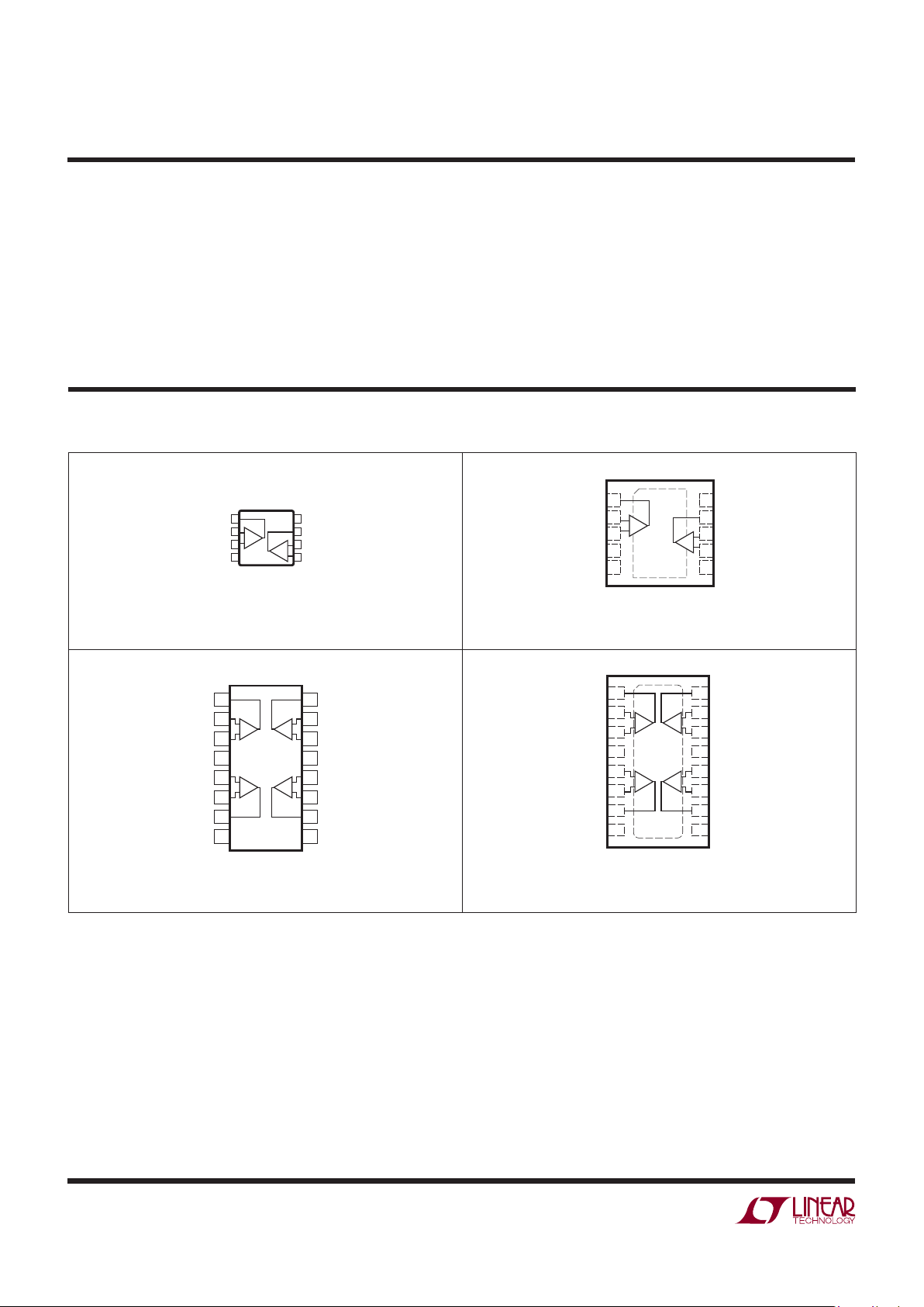
The dual amplifi er LTC6087 is available in 8-lead MSOP
and 10-lead DFN packages. The quad amplifi er LTC6088
is available in 16-lead SSOP and DFN packages.
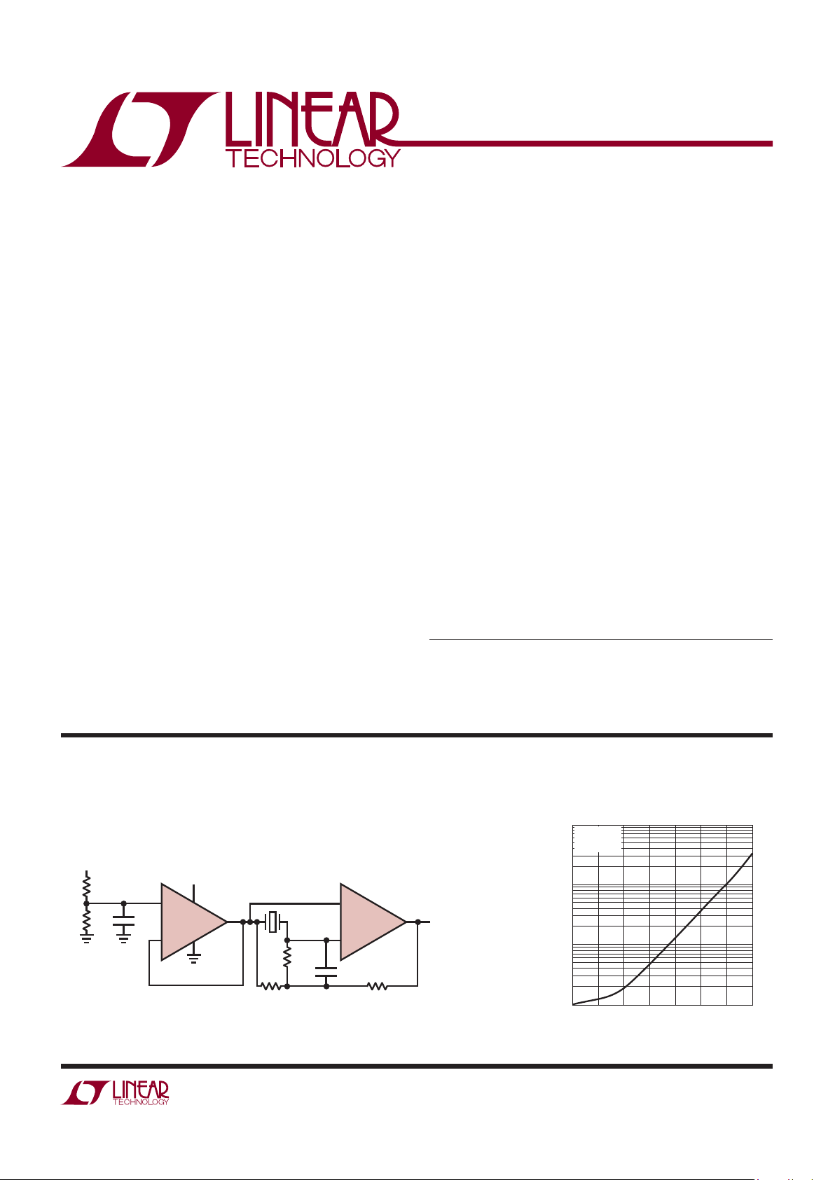
Single Supply Shock/Vibration Sensor Amplifi er
n
Low Offset Voltage: 750μV Maximum
n
Low Offset Drift: 5μV/°C Maximum
n
Input Bias Current:
1pA (Typical at 25°C)
15pA (Typical at 85°C)
n
Rail-to-Rail Inputs and Outputs
n
Gain Bandwidth Product: 14MHz
n
CMRR: 70dB Minimum
n
PSRR: 93dB Minimum
n
Input Noise Voltage Density: 12nV/√Hz
n
Supply Current: 1.1mA per Amp
n
Shutdown Current: 2.3μA per Amp
n
2.7V to 5.5V Operation Voltage
n
Available in 8-Lead MSOP and 10-Lead DFN
Packages (LTC6087), 16-Lead SSOP and DFN
Packages (LTC6088)
n
Portable Test Equipment
n
Medical Equipment
n
Audio
n
Data Acquisition
n
High Impedance Transducer Amplifi er
LTC6087 Input Bias Current
vs Temperature
L, LT, LTC and LTM are registered trademarks of Linear Technology Corporation. All other
trademarks are the property of their respective owners.
TYPICAL APPLICATION
–
+
1/2 LTC6087
MURATA SHOCK
SENSOR
PKGS-00MX1
520pF, 0.57pC/g
www.murata.com
–
+
1/2 LTC6087
V
S
1k
1%
100k
1%
60878 TA01a
V
OUT
570mV/g
16Hz TO 10kHz
V
S
= 2.7V TO 5.5V
V
S
0.1μF100k
100k
100M
100pF
TEMPERATURE (°C)
25 40
INPUT BIAS CURRENT (pA)
10
100
1000
VS = 5V
V
CM
= 2.5V
55 70 85 100 115 130
60878 TA01b
1
Page 2
LTC6087/LTC6088
2
60878fa
ABSOLUTE MAXIMUM RATINGS
Total Supply Voltage (V+ to V–) ...................................6V
Input Voltage ...................................................... V
–
to V
+
Output Short-Circuit Duration (Note 2) ............ Indefi nite
Operating Temperature Range (Note 3)
LTC6087C/LTC6088C ...........................–40°C to 85°C
LTC6087H/LTC6088H .........................–40°C to 125°C
(Note 1)
1
2
3
4
OUTA
–INA
+INA
V
–
8
7
6
5
V+
OUTB
–INB
+INB
TOP VIEW
MS8 PACKAGE
8-LEAD PLASTIC MSOP
+
–
A
+
–
B
T
JMAX
= 150°C, θJA = 200°C/W
TOP VIEW
11
DD PACKAGE
10-LEAD
(
3mm × 3mm) PLASTIC DFN
10
9
6
7
8
4
5
3
2
1
V+
OUTB
–INB
+INB
SHDNB
OUTA
–INA
+INA
V–
SHDNA
+
–
A
+
–
B
T
JMAX
= 150°C, θJA = 43°C/W
EXPOSED PAD (PIN 11) IS V
–
, MUST BE SOLDERED TO PCB
GN PACKAGE
16-LEAD PLASTIC SSOP NARROW
1
2
3
4
5
6
7
8
TOP VIEW
16
15
14
13
12
11
10
9
OUTA
–INA
+INA
V
+
+INB
–INB
OUTB
NC
OUTD
–IND
+IND
V
–
+INC
–INC
OUTC
NC
+
–
+
–
+
–
+
–
A
BC
D
T
JMAX
= 150°C, θJA = 110°C/W
16
15
14
13
12
11
10
9
17
1
2
3
4
5
6
7
8
OUTD
–IND
+IND
V
–
+INC
–INC
OUTC
NC
OUTA
–INA
+INA
V
+
+INB
–INB
OUTB
NC
TOP VIEW
DHC PACKAGE
16-LEAD
(
5mm × 3mm) PLASTIC DFN
+
–
+
–
+
–
+
–
A
BC
D
T
JMAX
= 150°C, θJA = 43°C/W
EXPOSED PAD (PIN 17) IS V
–
, MUST BE SOLDERED TO PCB
Specifi ed Temperature Range (Note 4)
LTC6087C/LTC6088C ...............................0°C to 70°C
LTC6087H/LTC6088H .........................–40°C to 125°C
Junction Temperature ........................................... 150°C
Storage Temperature Range ...................–65°C to 150°C
Lead Temperature (Soldering, 10 sec)
MS8, GN16 Only ............................................... 300°C
PIN CONFIGURATION
Page 3
LTC6087/LTC6088
3
60878fa
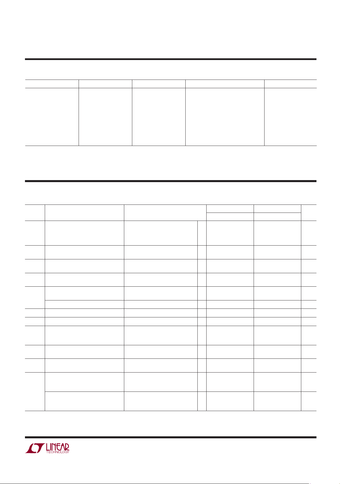
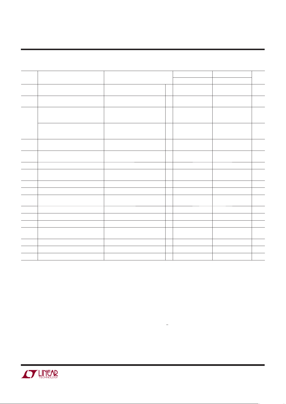
ORDER INFORMATION
The l denotes the specifi cations which apply over the full specifi ed
temperature range, otherwise specifi cations are at TA = 25°C. Test conditions are V+ = 3V, V– = 0V, VCM = 0.5V unless otherwise noted.
SYMBOL PARAMETER CONDITIONS
C SUFFIX H SUFFIX
UNITSMIN TYP MAX MIN TYP MAX
V
OS
Offset Voltage (Note 5) LTC6087MS8, LTC6088GN
LTC6087DD, LTC6088DHC
LTC6087MS8, LTC6088GN
LTC6087DD, LTC6088DHC
l
l
±330
±330
±750
±1100
±900
±1350
±330
±330
±750
±1100
±1100
±1600
μV
μV
μV
μV
ΔV
OS
/ΔT Input Offset Voltage Drift (Note 6) LTC6087MS8, LTC6088GN
LTC6087DD, LTC6088DHC
l
l
±2±2±5
±5
±2±2±5±5μV/°C
μV/°C
I
B
Input Bias Current (Notes 5, 7) Guaranteed by 5V Test
●
1
40
1
500
pA
pA
I
OS
Input Offset Current (Notes 5, 7) Guaranteed by 5V Test
●
0.5
30
0.5
150
pA
pA
e
n
Input Noise Voltage Density f = 1kHz
f = 10kHz
12
10
12
10
nV/√Hz
nV/√Hz
Input Noise Voltage 0.1Hz to 10Hz 2.5 2.5 μV
P-P
i
n
Input Noise Current Density (Note 8) f = 1Hz 0.56 0.56 fA/√Hz
Input Common Mode Range
●
V
–
V
+
V
–
V
+
V
C
IN
Input Capacitance
Differential Mode
Common Mode
f = 100kHz
2.7
4.2
2.7
4.2
pF
pF
CMRR Common Mode Rejection Ratio 0V ≤ V
CM
≤ 3V
●
646380 646180 dB
dB
PSRR Power Supply Rejection Ratio V
S
= 2.7V to 5.5V
●
9390115 9385115 dB
dB
V
OUT
Output Voltage, High (Referred to V+) No Load
I
SOURCE
= 1mA
I
SOURCE
= 5mA
●
●
●
5
25
120
15
50
210
5
25
120
20
50
230
mV
mV
mV
Output Voltage, Low (Referred to V
–
) No Load
I
SINK
= 1mA
I
SINK
= 5mA
●
●
●
5
25
120
25
50
210
5
25
120
30
60
240
mV
mV
mV
LEAD FREE FINISH TAPE AND REEL PART MARKING* PACKAGE DESCRIPTION TEMPERATURE RANGE
LTC6087CDD#PBF
LTC6087HDD#PBF
LTC6087CMS8#PBF
LTC6087HMS8#PBF
LTC6088CDHC#PBF
LTC6088HDHC#PBF
LTC6088CGN#PBF
LTC6088HGN#PBF
LTC6087CDD#TRPBF
LTC6087HDD#TRPBF
LTC6087CMS8#TRPBF
LTC6087HMS8#TRPBF
LTC6088CDHC#TRPBF
LTC6088HDHC#TRPBF
LTC6088CGN#TRPBF
LTC6088HGN#TRPBF
LCTX
LCTX
LT C T Y
LT C T Y
6088
6088
6088
6088H
10-Lead (3mm × 3mm) Plastic DFN
10-Lead (3mm × 3mm) Plastic DFN
8-Lead Plastic MSOP
8-Lead Plastic MSOP
16-Lead (5mm × 3mm) Plastic DFN
16-Lead (5mm × 3mm) Plastic DFN
16-Lead Plastic SSOP
16-Lead Plastic SSOP
–40°C to 85°C
–40°C to 125°C
–40°C to 85°C
–40°C to 125°C
–40°C to 85°C
–40°C to 125°C
–40°C to 85°C
–40°C to 125°C
Consult LTC Marketing for parts specifi ed with wider operating temperature ranges. *The temperature grade is identifi ed by a label on the shipping container.
Consult LTC Marketing for information on non-standard lead based fi nish parts.
For more information on lead free part marking, go to: http://www.linear.com/leadfree/
For more information on tape and reel specifi cations, go to: http://www.linear.com/tapeandreel/
ELECTRICAL CHARACTERISTICS
Page 4
LTC6087/LTC6088
4
60878fa
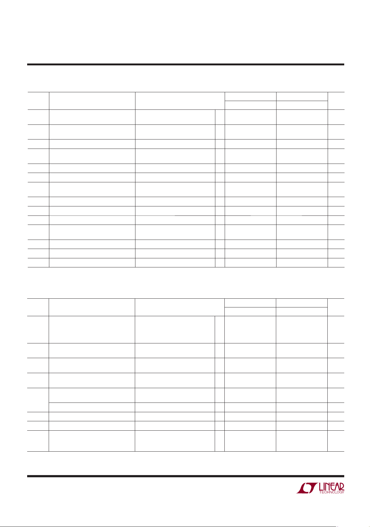
ELECTRICAL CHARACTERISTICS
The l denotes the specifi cations which apply over the full specifi ed
temperature range, otherwise specifi cations are at T
A
= 25°C. Test conditions are V+ = 3V, V– = 0V, VCM = 0.5V unless otherwise noted.
SYMBOL PARAMETER CONDITIONS
C SUFFIX H SUFFIX
UNITSMIN TYP MAX MIN TYP MAX
A
VOL
Large-Signal Voltage Gain R
LOAD
= 10k, 0.5V ≤ V
OUT
≤ 2.5V
●
500
300
3000 500303000 V/mV
V/mV
ISC Output Short-Circuit Current Source and Sink
●
252135 251835 mA
mA
SR Slew Rate AV = 1 7.2 7.2 V/μs
GBW Gain Bandwidth Product (f
TEST
= 20kHz) R
LOAD
= 50k
●
10914 10814 MHz
MHz
Φ
0
Phase Margin RL = 10k, CL = 45pF, AV = 1 45 45 Deg
t
S
Settling Time 0.1% V
STEP
= 2V, AV = –1, RL = 1k 1 1 μs
I
S
Supply Current (per Amplifi er) No Load
●
0.85
0.80
1.05
1.05
1.20
1.25
0.85
0.75
1.05
1.05
1.20
1.35
mA
mA
Shutdown Current (per Amplifi er) Shutdown, V
SHDN
≤ 0.8V
●
0.2 1 0.2 1 μA
V
S
Supply Voltage Range Guaranteed by the PSRR Test
●
2.7 5.5 2.7 5.5 V
Channel Separation f
S
= 10kHz –120 –120 dB
Shutdown Logic SHDN High
SHDN Low
●
●
2
0.8
2
0.8
V
V
t
ON
Turn-On Time V
SHDN
= 0.8V to 2V 6 6 μs
t
OFF
Turn-Off Time V
SHDN
= 2V to 0.8V 2 2 μs
Leakage of SHDN Pin V
SHDN
= 0V
●
0.1 0.5 0.1 0.5 μA
The l denotes the specifi cations which apply over the full specifi ed temperature range, otherwise specifi cations are at TA = 25°C.
Test conditions are V+ = 5V, V– = 0V, VCM = 0.5V unless otherwise noted.
SYMBOL PARAMETER CONDITIONS
C SUFFIX H SUFFIX
UNITSMIN TYP MAX MIN TYP MAX
V
OS
Offset Voltage (Note 5) LTC6087MS8, LTC6088GN
LTC6087DD, LTC6088DHC
LTC6087MS8, LTC6088GN
LTC6087DD, LTC6088DHC
l
l
±330
±330
±750
±1100
±900
±1350
±330
±330
±750
±1100
±1100
±1600
μV
μV
μV
μV
ΔV
OS
/ΔT Input Offset Voltage Drift (Note 6) LTC6087MS8, LTC6088GN
LTC6087DD, LTC6088DHC
l
l
±2±2±5
±5
±2±2±5±5μV/°C
μV/°C
I
B
Input Bias Current (Notes 5, 7)
●
1
40
1
500
pA
nA
I
OS
Input Offset Current (Notes 5, 7)
●
0.5
30
0.5
150
pA
pA
e
n
Input Noise Voltage Density f = 1kHz
f = 10kHz
12
10
12
10
nV/√Hz
nV/√Hz
Input Noise Voltage 0.1Hz to 10Hz 2.5 2.5 μV
P-P
i
n
Input Noise Current Density (Note 8) f = 1Hz 0.56 0.56 fA/√Hz
Input Common Mode Range
●
V
–
V
+
V
–
V
+
V
C
IN
Input Capacitance
Differential Mode
Common Mode
f = 100kHz
2.7
4.2
2.7
4.2
pF
pF
Page 5
LTC6087/LTC6088
5
60878fa
ELECTRICAL CHARACTERISTICS
The l denotes the specifi cations which apply over the full specifi ed
temperature range, otherwise specifi cations are at T
A
= 25°C. Test conditions are V+ = 5V, V– = 0V, VCM = 0.5V unless otherwise noted.
SYMBOL PARAMETER CONDITIONS
C SUFFIX H SUFFIX
UNITSMIN TYP MAX MIN TYP MAX
CMRR Common Mode Rejection Ratio 0V ≤ V
CM
≤ 5V
●
706884 706684 dB
dB
PSRR Power Supply Rejection Ratio VS = 2.7V to 5.5V
●
9390115 9385115 dB
dB
V
OUT
Output Voltage, High (Referred to V+) No Load
I
SOURCE
= 1mA
I
SOURCE
= 5mA
●
●
●
5
20
110
15
50
190
5
20
110
20
50
210
mV
mV
mV
Output Voltage, Low (Referred to V
–
) No Load
I
SINK
= 1mA
I
SINK
= 5mA
●
●
●
5
20
110
25
50
200
5
20
110
30
60
220
mV
mV
mV
A
VOL
Large-Signal Voltage Gain R
LOAD
= 10k, 0.5V ≤ V
OUT
≤ 4.5V
●
1000
500
6000 1000506000 V/mV
V/mV
ISC Output Short-Circuit Current Source and Sink
●
282545 282245 mA
mA
SR Slew Rate AV = 1 7.2 7.2 V/μs
GBW Gain Bandwidth Product (f
TEST
= 20kHz) R
LOAD
= 50k
●
10914 10814 MHz
MHz
Φ
0
Phase Margin RL = 10k, CL = 45pF, AV = 1 47 47 Deg
t
S
Settling Time 0.1% V
STEP
= 2V, AV = –1, RL = 1k 0.8 0.8 μs
I
S
Supply Current (per Amplifi er) No Load
●
0.85
0.80
1.05
1.05
1.25
1.30
0.85
0.75
1.05
1.05
1.25
1.40
mA
mA
Shutdown Current (per Amplifi er) Shutdown, V
SHDN
≤ 1.2V
●
2.3 5 2.3 5 μA
V
S
Supply Voltage Range Guaranteed by the PSRR Test
●
2.7 5.5 2.7 5.5 V
Channel Separation f
S
= 10kHz –120 –120 dB
Shutdown Logic SHDN High
SHDN Low
●
●
3.5
1.2
3.5
1.2
V
V
t
ON
Turn-On Time V
SHDN
= 1.2V to 3.5V 6 6 μs
t
OFF
Turn-Off Time V
SHDN
= 3.5V to 1.2V 2 2 μs
Leakage of SHDN Pin V
SHDN
= 0V
●
0.4 1 0.4 1 μA
Note 1: Stresses beyond those listed under Absolute Maximum Ratings
may cause permanent damage to the device. Exposure to any Absolute
Maximum Rating condition for extended periods may affect device
reliability and lifetime.
Note 2: A heat sink may be required to keep the junction temperature
below the absolute maximum. This depends on the power supply voltage
and the total output current.
Note 3: The LTC6087C/LTC6088C are guaranteed functional over the
operating temperature range of –40°C to 85°C. The LTC6087H/LTC6088H
are guaranteed functional over the operating temperature range of –40°C
to 125°C.
Note 4: The LTC6087C/LTC6088C are guaranteed to meet specifi ed
performance from 0°C to 70°C. The LTC6087C/LTC6088C are designed,
characterized and expected to meet specifi ed performance from –40°C to
125ºC but are not tested or QA sampled at these temperatures.
The LTC6087H/LTC6088H are guaranteed to meet specifi ed performance
from –40°C to 125°C.
Note 5: ESD (electrostatic discharge) sensitive device. ESD protection
devices are used extensively internal to the LTC6087/LTC6088; however,
high electrostatic discharge can damage or degrade the device. Use proper
ESD handling precautions.
Note 6: This parameter is not 100% tested.
Note 7: This specifi cation is limited by high speed automated test
capability. See Typical Performance Characteristic curves for actual
performance.
Note 8: Current noise is calculated from:
i
n
= √2qIB,
where q = 1.6 • 10
–19
coulombs.
Page 6

LTC6087/LTC6088
6
60878fa
TYPICAL PERFORMANCE CHARACTERISTICS
VOS Distribution VOS vs V
CM
VOS Drift Distribution
Input Bias Current vs
Common Mode Voltage Input Noise Voltage vs Frequency
0.1Hz to 10Hz Output Voltage
Noise
Output Voltage Swing vs
Load Current
Supply Current vs Supply Voltage
Input Noise Current vs Frequency
VOS (mV)
–1
0
PERCENTAGE OF UNITS (%)
2
4
6
8
12
–0.7
–0.4 –0.1 0.2 0.5
60878 G01
0.8
10
LTC6087MS8
V
S
= 5V
V
CM
= 0.5V
T
A
= 25°C
VCM (V)
0
V
OS
(mV)
0.2
0.6
1.0
4
60878 G02
–0.2
–0.6
0
0.4
0.8
–0.4
–0.8
–1.0
10.5
21.5
3 3.5 4.5
2.5
5
VS = 5V
T
A
= 25°C
REPRESENTATIVE PARTS
DISTRIBUTION (μV/°C)
–2
PERCENT OF UNITS (%)
14
16
18
20
22
1.2
60878 G03
8
10
12
2
4
6
0
–1.2
–0.4
0.4
2.0
2.8
LTC6087MS8
V
S
= 5V
V
CM
= 2.5V
T
A
= –40°C TO 125°C
COMMON MODE VOLTAGE (V)
0 0.5
INPUT BIAS CURRENT (pA)
0.1
1
10
100
1.5 2.5 3.512344.55
60878 G05
0.01
1000
10000
VS = 5V
TA = 125°C
TA = 85°C
TA = 25°C
FREQUENCY (Hz)
30
90
100
20
10
80
50
70
60
40
10 1k 10k 100k
60878 G06
0
100
INPUT NOISE VOLTAGE (nV/√Hz)
VS = 5V
V
CM
= 2.5V
T
A
= 25°C
TIME (1s/DIV)
INPUT NOISE VOLTAGE (1μV/DIV)
60878 G07
VS = 5V
V
CM
= 2.5V
FREQUENCY (Hz)
100
NOISE CURRENT (fA/√Hz)
200
300
400
500
1 100 1000 100000
60878 G04
0
10
10000
LOAD CURRENT (mA)
0.1
2.0
OUTPUT VOLTAGE SWING (V)
2.5
3.0
3.5
4.0
1 10 100
60878 G08
1.5
1.0
0.5
0
4.5
5.0
VS = 5V
V
CM
= 2.5V
TA = 125°C
T
A
= 25°C
T
A
= –55°C
SOURCE
SINK
SUPPLY VOLTAGE (V)
0
SUPPLY CURRENT (mA)
0.4
0.8
1.2
0.2
0.6
1.0
1234
69878 G09
5.50.50 1.5 2.5 3.5 4.5 5
PER AMPLIFIER
V
CM
= 0.5V
T
A
= 25°C
Page 7

LTC6087/LTC6088
7
60878fa
TYPICAL PERFORMANCE CHARACTERISTICS
Supply Current vs Temperature Open-Loop Gain vs Frequency CMRR vs Frequency
PSRR vs Frequency Output Impedance vs Frequency Small-Signal Response
Small-Signal Response Large-Signal Response Large-Signal Response
TEMPERATURE (°C)
–25
SUPPLY CURRENT (mA)
1.1
1.3
1.5
95
60878 G10
0.9
0.7
1.0
1.2
1.4
0.8
0.6
0.5
5
35
65
–10–40 110
20
50
80
125
PER AMPLIFIER
V
CM
= 0.5V
VS = 5V
VS = 3V
FREQUENCY (Hz)
10
GAIN (dB)
PHASE (DEG)
70
80
0
–10
60
30
50
40
20
10k 1M 10M 100M
60878 G11
–20
–20
100
120
–40
–60
80
20
60
40
0
–80
100k
VS = 5V
V
S
= 3V
CL = 5pF
R
L
= 1k
V
CM
= VS/2
T
A
= 25°C
PHASE
GAIN
FREQUENCY (Hz)
10
20
CMRR (dB)
30
40
50
70
60
100
90
80
10k 1M 10M 100M
60878 G12
–10
0
100k
110
VS = 5V
V
CM
= 2.5V
R
L
= 1k
T
A
= 25°C
FREQUENCY (Hz)
1k
40
PSRR (dB)
50
60
70
80
10k 100k 1M 10M 100M
60878 G13
30
20
10
0
–10
90
100
POSITIVE
SUPPLY
VS = 5V
V
CM
= 2.5V
T
A
= 25°C
NEGATIVE
SUPPLY
FREQUENCY (Hz)
10k 100k
0.001
OUTPUT IMPEDANCE (Ω)
1
1000
1M 10M 100M
60878 G14
0.1
0.01
10
100
VS = 5V
V
CM
= 2.5V
T
A
= 25°C
AV = 10
AV = 1
AV = 2
200ns/DIVVS = 5V
A
V
= 1
R
L
= ∞
60878 G15
100mV/DIV
200ns/DIVVS = 5V
A
V
= 1
R
L
= ∞
C
L
= 33pF
100mV/DIV
60878 G16
2μs/DIVVS = 5V
A
V
= 1
R
L
= ∞
1V/DIV
60878 G17
1μs/DIVVS = 5V
A
V
= –1
R
L
= 1k
1V/DIV
60878 G18
Page 8

LTC6087/LTC6088
8
60878fa
TYPICAL PERFORMANCE CHARACTERISTICS
Overshoot vs Capacitive Load
Channel Separation vs Frequency
Total Harmonic Distortion + Noise
vs Load Resistance
Total Harmonic Distortion + Noise
vs Frequency
Total Harmonic Distortion + Noise
vs Output Voltage
Disabled Output Impedance
vs Frequency
Overshoot vs Capacitive Load
Total Harmonic Distortion + Noise
vs Frequency
FREQUENCY (Hz)
10
OUTPUT IMPEDANCE (kΩ)
100
1000
100000
1000000
100 10k 100k 10M
60878 G20
1
1k
1M
10000
0.1
VS = 5V
V
CM
= 1V
A
V
= 1
T
A
= 25°C
CAPACITIVE LOAD (pF)
10
0
OVERSHOOT (%)
50
40
30
20
10
60
80
100 1000
60878 G21
70
VS = 5V
V
CM
= 2.5V
A
V
= 1
+
–
R
S
C
L
RS = 10Ω
RS = 50Ω
CAPACITIVE LOAD (pF)
10
0
OVERSHOOT (%)
25
20
15
10
5
30
40
100 1000
60878 G22
35
VS = 5V
V
CM
= 2.5V
A
V
= –1
RS = 10Ω
RS = 50Ω
R
S
1k
1k
30pF
C
L
+
–
FREQUENCY (MHz)
–120
CHANNEL SEPARATON (dB)
–110
–105
–95
–90
0.01 1 10 100
60878 G23
–130
0.1
–100
–115
–125
VS = 5V
V
CM
= 2.5V
T
A
= 25°C
FREQUENCY (kHz)
0.01
THD + NOISE (%)
0.1
0.01 1 10 100
60878 G24
0.001
0.1
1
AV = 1, VIN = 1V
P-P
AV = –2, VIN = 1V
P-P
AV = 1, VIN = 2V
P-P
AV = 2, VIN = 1V
P-P
VS = 3V
V
CM
= 1.5V
R
L
= 10k
FREQUENCY (kHz)
0.01
0.001
THD + NOISE (%)
0.01
0.1
10.1 10 100
60878 G25
AV = 1, VIN = 1V
P-P
AV = –2, VIN = 1V
P-P
AV = 1, VIN = 2V
P-P
AV = 2, VIN = 1V
P-P
VS = 5V
V
CM
= 2.5V
R
L
= 10k
OUTPUT VOLTAGE (V
P-P
)
0 0.5 1 2 2.5 3 4 4.5
0.0001
THD + NOISE (%)
0.01
0.1
1.5 3.5 5
60878 G26
0.001
VS = 3V
AT 20kHz
VS = 5V
AT 20kHz
VS = 5V
AT 1kHz
VS = 3V
AT 1kHz
RL = 10k
V
CM
= VS/2
A
V
= 1
LOAD RESISTANCE TO GROUND (kΩ)
0.1
0.0001
THD + NOISE (%)
0.001
0.01
0.1
1 10 100
60878 G27
VS = 3V, VIN = 1V
P-P
AV = 1
V
CM
= VS/2 AT 1kHz
VS = 5V, VIN = 2V
P-P
Page 9

LTC6087/LTC6088
9
60878fa
PIN FUNCTIONS
OUT: Amplifi er Output.
–IN: Inverting Input.
+IN: Noninverting Input.
V
+
: Positive Supply.
V–: Negative Supply.
SHDN A: Shutdown Pin of Amplifi er A, active low and only
available with the LTC 6087DD. An internal current source
pulls the pin to V
+
when fl oating.
SHDN B: Shutdown Pin of Amplifi er B, active low and only
available with the LTC 6087DD. An internal current source
pulls the pin to V
+
when fl oating.
NC: Not internally connected
Exposed Pad: Connected to V
–
.
Rail-to-Rail Input
The input stage of LTC6087/LTC6088 combines both PMOS
and NMOS differential pairs, extending its input common
mode voltage to both positive and negative supply voltages.
At high input common mode range, the NMOS pair is on.
At low common mode range, the PMOS pair is on. The
transition happens when the common voltage is between
1.3V and 0.9V below the positive supply.
Achieving Low Input Bias Current
The DD and DHC packages are leadless and make contact
to the PCB beneath the package. Solder fl ux used during
the attachment of the part to the PCB can create leakage
current paths and can degrade the input bias current performance of the part. All inputs are susceptible because
the backside paddle is connected to V
–
internally. As the
input voltage or V
–
changes, a leakage path can be formed
and alter the observed input bias current. For lowest bias
current use the LTC6087/LTC6088 in the leaded MSOP/GN
package. With fi ne PCB design rules, you can also provide
a guard ring around the inputs.
For example, in high source impedance applications such
as pH probes, photo diodes, strain gauges, et cetera, the
low input bias current of these parts requires a clean
board layout to minimize additional leakage current into a
high impedance signal node. A mere 100GΩ of PC board
resistance between a 5V supply trace and input trace near
ground potential adds 50pA of leakage current. This leakage is far greater than the bias current of the operational
amplifi er. A guard ring around the high impedance input
traces driven by a low impedance source equal to the
input voltage prevents such leakage problems. The guard
ring should extend as far as necessary to shield the high
impedance signal from any and all leakage paths. Figure 1
shows the use of a guard ring in a unity-gain confi guration.
In this case the guard ring is connected to the output and
is shielding the high impedance noninverting input from
V
–
. Figure 2 shows the inverting gain confi guration.
Figure 1. Sample Layout. Unity-Gain Confi guration. Using Guard
Ring to Shield High Impedance Input from Board Leakage
Figure 2. Sample Layout. Inverting Gain Confi guration. Using
Guard Ring to Shield High Impedance Input from Board Leakage
APPLICATIONS INFORMATION
LTC6087
R
OUT
IN
–
IN
+
V
–
LEAKAGE
CURRENT
NO LEAKAGE
CURRENT
GUARD
RING
NO SOLDER MASK
OVER THE GUARD RING
60878 F01
LTC6087
60878 F02
R
R
OUT
IN
–
IN
+
V
–
V
IN
GND
Page 10

LTC6087/LTC6088
10
60878fa
APPLICATIONS INFORMATION
Rail-to-Rail Output
The output stage of the LTC6087/LTC6088 swings within
30mV of the supply rails when driving high impedance
loads, in other words when no DC load current is present.
See the Typical Performance Characteristics for curves of
output swing versus load current. The class AB design of
the output stage enables the op amp to supply load currents which are much greater than the quiescent supply
current. For example, the room temperature short circuit
current is typically 45mA.
Capacitive Load
LTC6087/LTC6088 can drive capacitive load up to 100pF in
unity gain. The capacitive load driving capability increases
as the amplifi er is used in higher gain confi gurations. A
small series resistance between the output and the load
further increases the amount of capacitance the amplifi er
can drive.
SHDN Pins
Pins 5 and 6 are used for power shutdown when the
LTC6087 is in the DD package. If they are fl oating, internal
current sources pull Pins 5 and 6 to V
+
and the amplifi ers
operate normally. In shutdown the amplifi er output is
high impedance and each amplifi er draws less than 5μA
current. This feature allows the part to be used in muxed
output applications as shown in Figure 3.
ESD
The LTC6087/LTC6088 has reverse-biased ESD protection
diodes on all inputs and outputs as shown in the Simplifi ed
Schematic. If these pins are forced beyond either supply,
unlimited current will fl ow through these diodes. If the
current is transient and limited to one hundred milliamps
or less, no damage to the device will occur.
The amplifi er input bias current is the leakage current of
these ESD diodes. This leakage is a function of the temperature and common mode voltage of the amplifi er, as
shown in the Typical Performance Characteristics.
Noise
In the frequency region above 1kHz, the LTC6087/LTC6088
shows good noise voltage performance. In this region,
noise can be dominated by the total source resistance of the
particular application. Specifi cally, these amplifi ers exhibit
the noise of a 10k resistor, meaning it is desirable to keep
the source and feedback resistance at or below this value,
i.e., R
S
+ RG||RFB ≤ 10k. Above this total source impedance,
the noise voltage is dominated by the resistor.
At low frequency, noise current can be estimated from the
expression in = √2qI
B
, where q = 1.6 • 10
–19
coulombs.
Equating √4kTRΔf and R√2qI
B
Δf shows that for source
resistor below 50GΩ the amplifi er noise is dominated by
the source resistance. Noise current rises with frequency.
See the curve Noise Current vs Frequency in the Typical
Performance Characteristics section.
Figure 3. Inverting Amplifi er with Muxed Output
–
+
10k
10k
10k
10k
10pF
10pF
OUT
LTC6087
(DD PACKAGE)
SEL = 5V, OUT = –INA
SEL = 0V, OUT = –1NB
10k 10k
SHDN
A
SHDN
B
FAIRCHILD
NC7SZ04 OR
EQUIVALENT
5V
A
5V
INA
5V
10k
10k
5V
60878 F03
INB
SEL
–
+
B
Page 11

LTC6087/LTC6088
11
60878fa
SIMPLIFIED SCHEMATIC
R1 R2
R3
V
+
V
–
R4
–
+
D8
D7
OUT
M8
M9
C1
C2
60878 SS
V
+
V
–
D5
D6
–
+
OUTPUT
CONTROL
M4
M6
A1
A2
M7
M5
I
1
V
BIAS
M1 M2
M3
–IN
V
+
V
–
V
+
V
–
D3
D4
+IN
V
–
M11M10
1μA
V
+
V
–
D1
D2
SHDN
BIAS
GENERATION
NOTE: SHDN IS ONLY AVAILABLE
IN THE DFN10 PACKAGE
I
2
Page 12

LTC6087/LTC6088
12
60878fa
PACKAGE DESCRIPTION
MS8 Package
8-Lead Plastic MSOP
(Reference LTC DWG # 05-08-1660 Rev F)
MSOP (MS8) 0307 REV F
0.53 ± 0.152
(.021 ± .006)
SEATING
PLANE
NOTE:
1. DIMENSIONS IN MILLIMETER/(INCH)
2. DRAWING NOT TO SCALE
3. DIMENSION DOES NOT INCLUDE MOLD FLASH, PROTRUSIONS OR GATE BURRS.
MOLD FLASH, PROTRUSIONS OR GATE BURRS SHALL NOT EXCEED 0.152mm (.006") PER SIDE
4. DIMENSION DOES NOT INCLUDE INTERLEAD FLASH OR PROTRUSIONS.
INTERLEAD FLASH OR PROTRUSIONS SHALL NOT EXCEED 0.152mm (.006") PER SIDE
5. LEAD COPLANARITY (BOTTOM OF LEADS AFTER FORMING) SHALL BE 0.102mm (.004") MAX
0.18
(.007)
0.254
(.010)
1.10
(.043)
MAX
0.22 – 0.38
(.009 – .015)
TYP
0.1016 ± 0.0508
(.004 ± .002)
0.86
(.034)
REF
0.65
(.0256)
BSC
0° – 6° TYP
DETAIL “A”
DETAIL “A”
GAUGE PLANE
12
3
4
4.90 ± 0.152
(.193 ± .006)
8
7
6
5
3.00 ± 0.102
(.118 ± .004)
(NOTE 3)
3.00 ± 0.102
(.118 ± .004)
(NOTE 4)
0.52
(.0205)
REF
5.23
(.206)
MIN
3.20 – 3.45
(.126 – .136)
0.889 ± 0.127
(.035 ± .005)
RECOMMENDED SOLDER PAD LAYOUT
0.42 ± 0.038
(.0165 ± .0015)
TYP
0.65
(.0256)
BSC
Page 13

LTC6087/LTC6088
13
60878fa
PACKAGE DESCRIPTION
DD Package
10-Lead Plastic DFN (3mm × 3mm)
(Reference LTC DWG # 05-08-1699)
3.00 ±0.10
(4 SIDES)
NOTE:
1. DRAWING TO BE MADE A JEDEC PACKAGE OUTLINE M0-229 VARIATION OF (WEED-2).
CHECK THE LTC WEBSITE DATA SHEET FOR CURRENT STATUS OF VARIATION ASSIGNMENT
2. DRAWING NOT TO SCALE
3. ALL DIMENSIONS ARE IN MILLIMETERS
4. DIMENSIONS OF EXPOSED PAD ON BOTTOM OF PACKAGE DO NOT INCLUDE
MOLD FLASH. MOLD FLASH, IF PRESENT, SHALL NOT EXCEED 0.15mm ON ANY SIDE
5. EXPOSED PAD SHALL BE SOLDER PLATED
6. SHADED AREA IS ONLY A REFERENCE FOR PIN 1 LOCATION ON THE
TOP AND BOTTOM OF PACKAGE
0.38 ± 0.10
BOTTOM VIEW—EXPOSED PAD
1.65 ± 0.10
(2 SIDES)
0.75 ±0.05
R = 0.115
TYP
2.38 ±0.10
(2 SIDES)
15
106
PIN 1
TOP MARK
(SEE NOTE 6)
0.200 REF
0.00 – 0.05
(DD) DFN 1103
0.25 ± 0.05
2.38 ±0.05
(2 SIDES)
RECOMMENDED SOLDER PAD PITCH AND DIMENSIONS
1.65 ±0.05
(2 SIDES)2.15 ±0.05
0.50
BSC
0.675 ±0.05
3.50 ±0.05
PACKAGE
OUTLINE
0.25 ± 0.05
0.50 BSC
Page 14

LTC6087/LTC6088
14
60878fa
PACKAGE DESCRIPTION
GN Package
16-Lead Plastic SSOP (Narrow .150 Inch)
(Reference LTC DWG # 05-08-1641)
GN16 (SSOP) 0204
12
3
4
5
678
.229 – .244
(5.817 – 6.198)
.150 – .157**
(3.810 – 3.988)
16
15
14
13
.189 – .196*
(4.801 – 4.978)
12 11 10
9
.016 – .050
(0.406 – 1.270)
.015 ± .004
(0.38 ± 0.10)
×
45
°
0° – 8° TYP
.007 – .0098
(0.178 – 0.249)
.0532 – .0688
(1.35 – 1.75)
.008 – .012
(0.203 – 0.305)
TYP
.004 – .0098
(0.102 – 0.249)
.0250
(0.635)
BSC
.009
(0.229)
REF
.254 MIN
RECOMMENDED SOLDER PAD LAYOUT
.150 – .165
.0250 BSC.0165 ±.0015
.045 ±.005
*DIMENSION DOES NOT INCLUDE MOLD FLASH. MOLD FLASH
SHALL NOT EXCEED 0.006" (0.152mm) PER SIDE
**DIMENSION DOES NOT INCLUDE INTERLEAD FLASH. INTERLEAD
FLASH SHALL NOT EXCEED 0.010" (0.254mm) PER SIDE
INCHES
(MILLIMETERS)
NOTE:
1. CONTROLLING DIMENSION: INCHES
2. DIMENSIONS ARE IN
3. DRAWING NOT TO SCALE
Page 15

LTC6087/LTC6088
15
60878fa
Information furnished by Linear Technology Corporation is believed to be accurate and reliable.
However, no responsibility is assumed for its use. Linear Technology Corporation makes no representation that the interconnection of its circuits as described herein will not infringe on existing patent rights.
PACKAGE DESCRIPTION
DHC Package
16-Lead Plastic DFN (5mm × 3mm)
(Reference LTC DWG # 05-08-1706)
3.00 ±0.10
(2 SIDES)
5.00 ±0.10
(2 SIDES)
NOTE:
1. DRAWING PROPOSED TO BE MADE VARIATION OF VERSION (WJED-1) IN JEDEC
PACKAGE OUTLINE MO-229
2. DRAWING NOT TO SCALE
3. ALL DIMENSIONS ARE IN MILLIMETERS
4. DIMENSIONS OF EXPOSED PAD ON BOTTOM OF PACKAGE DO NOT INCLUDE
MOLD FLASH. MOLD FLASH, IF PRESENT, SHALL NOT EXCEED 0.15mm ON ANY SIDE
5. EXPOSED PAD SHALL BE SOLDER PLATED
6. SHADED AREA IS ONLY A REFERENCE FOR PIN 1 LOCATION ON THE
TOP AND BOTTOM OF PACKAGE
0.40 ± 0.10
BOTTOM VIEW—EXPOSED PAD
1.65 ± 0.10
(2 SIDES)
0.75 ±0.05
R = 0.115
TYP
R = 0.20
TYP
4.40 ±0.10
(2 SIDES)
18
169
PIN 1
TOP MARK
(SEE NOTE 6)
0.200 REF
0.00 – 0.05
(DHC16) DFN 1103
0.25 ± 0.05
PIN 1
NOTCH
0.50 BSC
4.40 ±0.05
(2 SIDES)
RECOMMENDED SOLDER PAD PITCH AND DIMENSIONS
1.65 ±0.05
(2 SIDES)2.20 ±0.05
0.50 BSC
0.65 ±0.05
3.50 ±0.05
PACKAGE
OUTLINE
0.25 ± 0.05
Page 16

LTC6087/LTC6088
16
60878fa
Linear Technology Corporation
1630 McCarthy Blvd., Milpitas, CA 95035-7417
(408) 432-1900 ● FAX: (408) 434-0507
●
www.linear.com
© LINEAR TECHNOLOGY CORPORATION 2007
LT 1207 REV A • PRINTED IN USA
PART NUMBER DESCRIPTION COMMENTS
LTC2051/LTC2052 Dual/Quad Zero-Drift Op Amps 3μV V
OS(MAX)
, 30nV/°C VOS Drift (MAX)
LTC6078/LTC6079 Dual/Quad Micropower Precision Rail-to-Rail Op Amps 25μV V
OS(MAX)
, 0.7μV/°C VOS Drift (MAX), 1pA I
BIAS(MAX)
LTC6240 Single Low Noise Rail-to-Rail Output Op Amp 7nV/√Hz Noise, 1pA I
BIAS(MAX)
, 10V/μs Slew Rate
LTC6241/LTC6242 Dual/Quad Low Noise Rail-to-Rail Output Op Amps 7nV/√Hz Noise, 0.2pA I
BIAS
, 18MHz Gain Bandwidth
LTC6244 Dual 50MHz Rail-to-Rail Op Amps 100μV V
OS(MAX)
, 1pA I
BIAS
, 40V/μs Slew Rate
TYPICAL APPLICATIONS
Negative-Going and Positive-Going Photodiode TIAs on ±5V Supplies
Almost Rail-to-Rail (0.3V to VCC) Gain-of-30 Current Sense Amplifi er
–
+
1/2 LTC6087
5V
5V
1.5k
–5V
I
PD
V
OUT
0V – IPD • R
F
R
F
100k
R
F
100k
1N4148
C
F
2pF
C
F
2pF
PHOTODIODE
~3pF
PHOTODIODE
~3pF
–
+
1/2 LTC6087
–5V
5V
1.5k
–5V
60878 TA02
I
PD
V
OUT
0V + IPD • R
F
1N4148
NOTE: DIFFERENT DEVICES.
NOT THE SAME LTC6087
–
+
1/2 LTC6087
–
+
1/2 LTC6087
GAIN OF 15 STAGE
GAIN OF 2 STAGE
140k
1%
10k
1%
OUT
200Ω
1%
60878 TA03
FULL-SCALE V
SENSE
= 100mV (3V OUT).
FOR SMALL SIGNALS, INPUT OPERATION IS
RAIL-TO-RAIL (V
S
= 5mV to VCC).
FOR FULL SCALE, INPUT OPERATION IS 0.3V TO RAIL.
WORST-CASE INPUT OFFSET VOLTAGE = 1.8mV.
2N7002
C
COMP
1nF
R
COMP
10k
V
CC
V
S
+–
LOAD
V
SENSE
I
SENSE
R
SENSE
100Ω
1%
RELATED PARTS
 Loading...