

Datasheet LTC485IN8, LTC485CS8, LTC485CN8, LTC485, LTC485MJ8 Datasheet (Linear Technology)
...Page 1
LTC485
Low Power RS485
Interface Transceiver
EATU
F
■
Low Power: ICC = 300µA Typ
■
Designed for RS485 Interface Applications
■
Single 5V supply
■
–7V to 12V Bus Common-Mode Range Permits
RE
S
±7V Ground Difference Between Devices on the Bus
■
Thermal Shutdown Protection
■
Power-Up/Down Glitch-Free Driver Outputs
Permit Live Insertion or Removal of Transceiver
■
Driver Maintains High Impedance in Three-State
or with the Power Off
■
Combined Impedance of a Driver Output and
Receiver Allows Up to 32 Transceivers on the Bus
■
70mV Typical Input Hysteresis
■
30ns Typical Driver Propagation Delays
with 5ns Skew
■
Pin Compatible with the SN75176A, DS75176A
and µA96176
U
O
PPLICATI
A
S
DUESCRIPTIO
The LTC485 is a low power differential bus/line transceiver
designed for multipoint data transmission standard RS485
applications with extended common-mode range (12V to
–7V). It also meets the requirements of RS422.
The CMOS design offers significant power savings over its
bipolar counterpart without sacrificing ruggedness against
overload of ESD damage.
The driver and receiver feature three-state outputs, with
the driver outputs maintaining high impedance over the
entire common-mode range. Excessive power dissipation
caused by bus contention or faults is prevented by a
thermal shutdown circuit which forces the driver outputs
into a high impedance state.
The receiver has a fail-safe feature which guarantees a
high output state when the inputs are left open.
The LTC485 is fully specified over the commercial and
extended industrial temperature range.
■
Low Power RS485/RS422 Transceiver
■
Level Translator
O
A
PPLICATITYPICAL
RO1
RE1
DE1
DI1
RO2
RE2
DE2
DI2
R
D
R
D
V
CC1
GND1
V
CC2
GND2
U
Rt
Rt
LTC485 • TA01
Driver Outputs
A
B
LTC485 • TA02
1
Page 2
LTC485
A
W
O
LUTEXI T
S
A
WUW
ARB
U
G
I
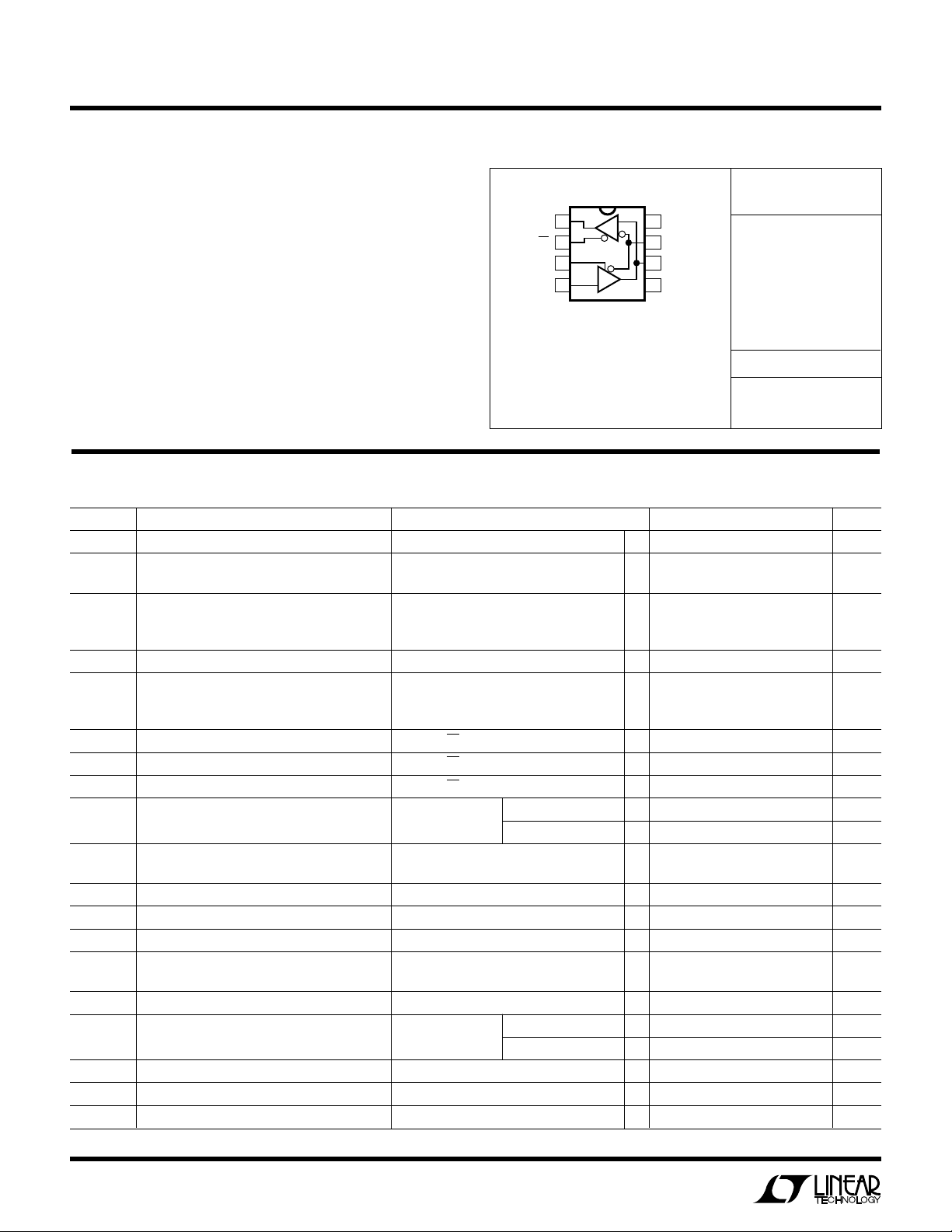
S
PACKAGE
/
O
RDER I FOR ATIO
WU
(Note 1)
Supply Voltage ....................................................... 12V
Control Input Voltages ................... – 0.5V to VCC + 0.5V
Driver Input Voltage....................... – 0.5V to VCC + 0.5V
Driver Output Voltage ........................................... ±14V
RO
RE
DE
Receiver Input Voltage.......................................... ±14V
Receiver Output Voltages .............. –0.5V to VCC + 0.5V
Operating Temperature Range
J8 PACKAGE
8-LEAD CERAMIC DIP
LTC485I...................................... –40°C ≤ TA ≤ 85°C
LTC485C.......................................... 0°C ≤ TA ≤ 70°C
LTC485M.................................. – 55°C ≤ TA ≤ 125°C
Lead Temperature (Soldering, 10 sec)................. 300°C
V
LECTRICAL C CHARA TERIST
E
SYMBOL PARAMETER CONDITIONS MIN TYP MAX UNITS
V
OD1
V
OD2
∆V
OD
V
OC
∆V
OC
V
IH
V
IL
I
IN1
I
IN2
V
TH
∆V
TH
V
OH
V
OL
I
OZR
R
IN
I
CC
I
OSD1
I
OSD2
I
OSR
Differential Driver Output Voltage (Unloaded) IO = 0 ● 5V
Differential Driver Output Voltage (with Load) R = 50Ω (RS422) ● 2V
Change in Magnitude of Driver R = 27Ω or R = 50Ω, Figure 1 ● 0.2 V
DifferentialOutput Voltage for
Complementary States
Driver Common-Mode Output Voltage R = 27Ω or R = 50Ω, Figure 1 ● 3V
Change in Magnitude of Driver R = 27Ω or R = 50Ω, Figure 1 ● 0.2 V
Common-Mode Output Voltage
for Complementary States
Input High Voltage DE, DI, RE ● 2V
Input Low Voltage DE, DI, RE ● 0.8 V
Input Current DE, DI, RE ● ±2 µA
Input Current (A, B) DE = 0, VCC = 0V VIN = 12V ● ±1mA
Differential Input Threshold Voltage –7V ≤ VCM ≤ 12V ● –0.2 0.2 V
for Receiver
Receiver Input Hysteresis VCM = 0V ● 70 mV
Receiver Output High Voltage IO = –4mA, VID = 200mV ● 3.5 V
Receiver Outpu Low Voltage IO = 4mA, VID = –200mV ● 0.4 V
Three-State (High Impedance) Output VCC = Max, 0.4V ≤ VO ≤ 2.4V ● ±1 µA
Current at Receiver
Receiver Input Resistance –7V ≤ VCM ≤ 12V ● 12 kΩ
Supply Current No Load, Pins 2, Outputs Enabled ● 500 900 µA
Driver Short-Circuit Current, V
Driver Short-Circuit Current, V
Receiver Short-Circuit Current 0V ≤ VO ≤ V
= HIGH VO = –7V ● 35 100 250 mA
OUT
= LOW VO = 10V ● 35 100 250 mA
OUT
ICS
= 5V ±5%, unless otherwise noted. (Notes 2 and 3)
CC
R = 27Ω (RS485), Figure 1
or 5.25V
3, 4 = 0V or 5V
CC
T
T
= –7V ● –0.8 mA
V
IN
Outputs Disabled
TOP VIEW
1
2
3
DI
T
JMAX
JMAX
JMAX
D
4
S8 PACKAGE
8-LEAD PLASTIC SOIC
= 155°C, θ
= 100°C, θ
= 100°C, θ
V
8
R
8-LEAD PLASTIC DIP
= 100°C/ W (J)
JA
= 130°C/ W (N)
JA
= 170°C/ W (S)
JA
CC
B
7
A
6
GND
5
N8 PACKAGE
● 1.5 5 V
● 300 500 µA
● 785mA
ORDER PART
NUMBER
LTC485CJ8
LTC485CN8
LTC485CS8
LTC485IN8
LTC485IS8
LTC485MJ8
S8 PART MARKING
485
485I
U
2
Page 3
LTC485
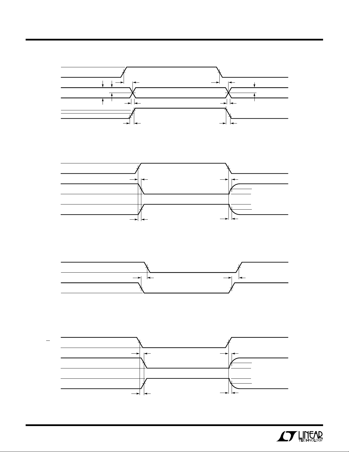
U
SWITCHI G CHARACTERISTICS
SYMBOL PARAMETER CONDITIONS MIN TYP MAX UNITS
t
PLH
t
PHL
t
SKEW
t
, t
r
f
tZHDriver Enable to Output High CL = 100pF (Figures 4 and 6) S2 Closed ● 40 70 ns
t
ZL
t
LZ
t
HZ
t
PLH
t
PHL
t
SKD
t
ZL
t
ZH
t
LZ
t
HZ
Driver Input to Output R
Driver Input to Output
Driver Output to Output ● 510ns
Driver Rise or Fall Time ● 31525ns
Driver Enable to Output Low CL = 100pF (Figures 4 and 6) S1 Closed ● 40 70 ns
Driver Disable Time from Low CL = 15pF (Figures 4 and 6) S1 Closed ● 40 70 ns
Driver Disable Time from High CL = 15pF (Figures 4 and 6) S2 Closed ● 40 70 ns
Receiver Input to Output R
t
– t
PLH
Differential Receiver Skew ● 13 ns
PHL
Receiver Enable to Output Low CRL = 15pF (Figures 2 and 8) S1 Closed ● 20 50 ns
Receiver Enable to Output High CRL = 15pF (Figures 2 and 8) S2 Closed ● 20 50 ns
Receiver Disable from Low CRL = 15pF (Figures 2 and 8) S1 Closed ● 20 50 ns
Receiver Disable from High CRL = 15pF (Figures 2 and 8) S2 Closed ● 20 50 ns
VCC = 5V ±5%, unless otherwise noted. (Notes 2 and 3)
= 54Ω, CL1 = CL2 = 100pF, ● 10 30 50 ns
DIFF
(Figures 3 and 5)
= 54Ω, CL1 = CL2 = 100pF, ● 30 90 200 ns
DIFF
(Figures 3 and 7)
● 10 30 50 ns
● 30 90 200 ns
The ● denotes specifications which apply over the full operating
temperature range.
Note 1: Absolute maximum ratings are those beyond which the safety of
the device cannot be guaranteed.
Note 2: All currents into device pins are positive; all currents out ot device
pins are negative. All voltages are referenced to device ground unless
otherwise specified.
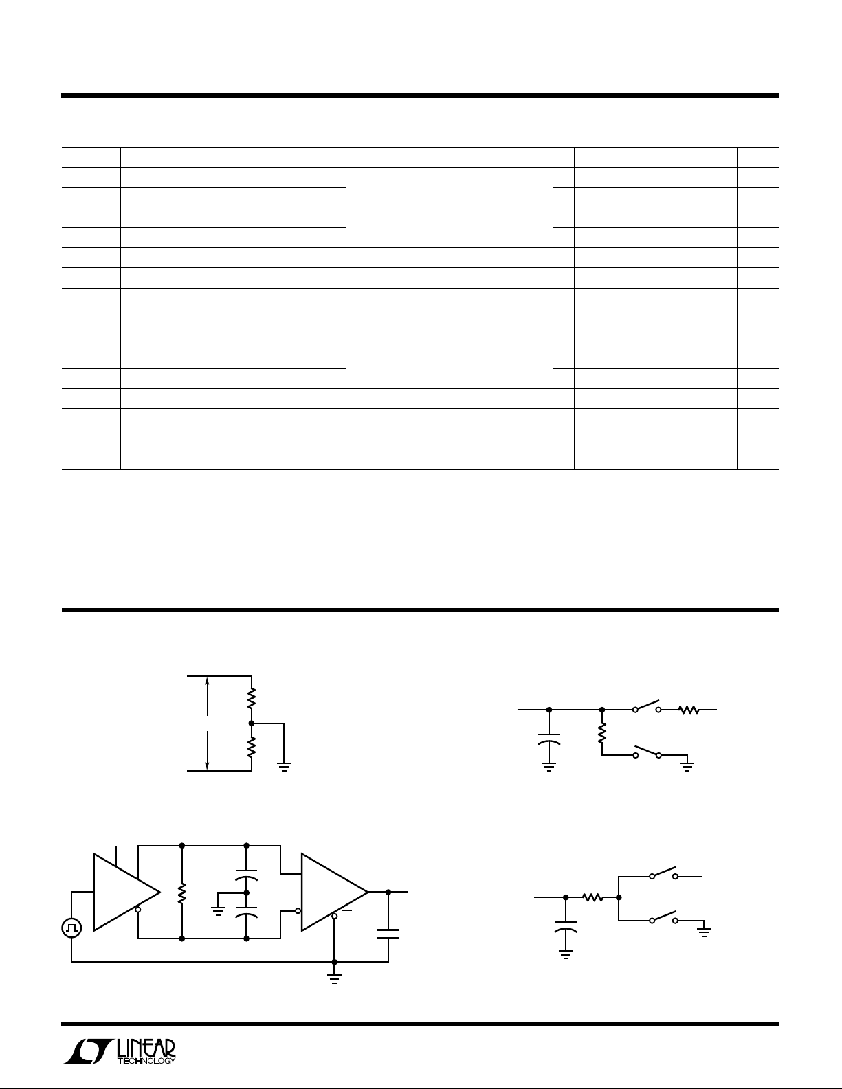
TEST CIRCUITS
A
R
V
OD
V
OC
R
B
Figure 1. Driver DC Test Load Figure 2. Receiver Timing Test Load
3V
DE
DI
A
B
LTC485 • F01
A
C
L1
R
DIFF
B
C
L2
RO
RE
15pF
LTC485 • F03
Note 3: All typicals are given for V
= 5V and TA = 25°C.
CC
Note 4: The LTC485 is guaranteed by design to be functional over a supply
voltage range of 5V ±10%. Data sheet parameters are guaranteed over the
tested supply voltage range of 5V ±5%.
RECEIVER
OUTPUT
OUTPUT
UNDER TEST
TEST POINT
C
RL
15pF
500Ω
C
L
S1
1k
V
CC
1k
S2
LTC485 • F02
S1
V
CC
S2
LTC485 • F02
Figure 3. Driver/Receiver Timing Test Circuit Figure 4. Driver Timing Test Load #2
3
Page 4
LTC485
UW W
SWITCHI G TI E WAVEFOR S
DI
A, B
A, B
–V
3V
0V
B
A
V
O
0V
O
V
O
1/2 V
1.5V
O
10%
t
r
f = 1MHz, tr ≤ 10ns, tf ≤ 10ns
t
PLH
t
SKEW
80%
V
DIFF
= V(A) – V(B)
t
PLH
1.5V
1/2 V
O
t
SKEW
90%
20%
t
f
LTC485 • F05
Figure 5. Driver Propagation Delays
3V
DI
0V
5V
V
OL
V
OH
0V
t
1.5V
t
ZL
ZH
f = 1MHz, tr ≤ 10ns, tf ≤ 10ns
2.3V
2.3V
OUTPUT NORMALLY LOW
OUTPUT NORMALLY HIGH
t
t
1.5V
LZ
0.5V
0.5V
HZ
LTC485 • F06
A, B
Figure 6. Driver Enable and Disable Times
V
–V
OH
R
V
OL
V
OD2
OD2
t
PHL
1.5V
f = 1MHz, tr ≤ 10ns, tf ≤ 10ns
0V
OUTPUT
INPUT
1.5V
t
PLH
LTC485 • F07
Figure 7. Receiver Propagation Delays
3V
RE
0V
5V
R
R
0V
t
1.5V
f = 1MHz, tr ≤ 10ns, tf ≤ 10ns
t
ZL
1.5V
1.5V
ZH
OUTPUT NORMALLY LOW
OUTPUT NORMALLY HIGH
t
t
1.5V
LZ
0.5V
0.5V
HZ
LTC485 • F08
4
Figure 8. Receiver Enable and Disable Times
Page 5

LTC485
TEMPERATURE (°C)
–50
3.0
OUTPUT VOLTAGE (V)
3.2
3.6
3.8
4.0
75
4.8
LTC485 • TPC03
3.4
0 125
4.2
4.4
4.6
–25
25 50
100
I = 8mA
UU
FU CTIO TABLES
LTC485 Transmitting
INPUTS OUTPUTS
RE DE DI B A
X 1 1 No Fault 0 1
X 1 0 No Fault 1 0
X0X X ZZ
X 1 X Fault Z Z
LTC485 Receiving
INPUTS OUTPUTS
RE DE A – B R
00≥0.2V 1
00≤–0.2V 0
0 0 Inputs Open 1
10 X Z
LINE
CONDITION
UU U
PI FU CTIO S
PIN # NAME DESCRIPTION
1 RO Receiver Output. If the receiver output is enabled
(RE low), then if A > B by 200mV, RO will be
high. If A < B by 200mV, then RO will be low.
2 RE Receiver Output Enable. A low enables the
receiver output, RO. A high input forces the
receiver output into a high impedance state.
3 DE Driver Outputs Enable. A high on DE enables the
driver output. A and B, and the chip will function
as a line driver. A low input will force the driver
outputs into a high impedance state and the chip
will function as a line receiver.
4 DI Driver Input. If the driver outputs are enabled
(DE high), then a low on DI forces the outputs A
low and B high. A high on DI with the driver
outputs enabled will force A high and B low.
5 GND Ground Connection.
6 A Driver Output/Receiver Input.
7 B Driver Output/Receiver Input.
8V
CC
Positive Supply; 4.75 < VCC < 5.25
36
32
28
24
20
16
12
OUTPUT CURRENT (mA)
8
4
0
LPER
F
O
R
Receiver Output Low Voltage
vs Output Current
TA = 25°C
0.5 2.0
0
OUTPUT VOLTAGE (V)
1.0
1.5
ATYPICA
LTC485 • TPC01
UW
CCHARA TERIST
E
C
Receiver Output High Voltage
vs Output Current
–18
TA = 25°C
–16
–14
–12
–10
–8
–6
OUTPUT CURRENT (mA)
–4
–2
0
5
ICS
4
OUTPUT VOLTAGE (V)
3
Receiver Output High Voltage
vs Temperature
2
LTC485 • TPC02
5
Page 6

LTC485
TEMPERATURE (°C)
–50
1.5
DIFFERENTIAL VOLTAGE (V)
1.6
1.8
1.9
2.0
75
2.4
LTC485 • TPC06
1.7
0 125
2.1
2.2
2.3
–25
25 50
100
RI = 54Ω
TEMPERATURE (°C)
–50
1.55
INPUT THRESHOLD VOLTAGE (V)
1.56
1.58
1.59
1.60
75
1.64
LTC485 • TPC09
1.57
0 125
1.61
1.62
1.63
–25
25 50
100
TEMPERATURE (°C)
–50
100
SUPPLY CURRENT (µA)
160
280
340
400
75
640
LTC485 • TPC12
220
0 125
460
520
580
–25
25 50
100
DRIVER ENABLED
DRIVER DISABLED
LPER
F
O
R
ATYPICA
UW
CCHARA TERIST
E
C
ICS
Receiver Output Low Voltage
vs Temperature
0.9
I = 8mA
0.8
0.7
0.6
0.5
0.4
0.3
OUTPUT VOLTAGE (V)
0.2
0.1
0
–50
–25
25 50
0 125
TEMPERATURE (°C)
Driver Output Low Voltage
vs Output Current
90
TA = 25°C
80
70
60
50
40
30
OUTPUT CURRENT (mA)
20
10
0
13
0
2
OUTPUT VOLTAGE (V)
75
LTC485 • TPC03
LTC485 • TPC07
100
Driver Differential Output Voltage
vs Output Current
72
TA = 25°C
64
56
48
40
32
24
OUTPUT CURRENT (mA)
16
8
0
13
0
2
OUTPUT VOLTAGE (V)
4
LTC485 • TPC05
Driver Output High Voltage
vs Output Current
–108
–96
–84
–72
–60
–48
–36
OUTPUT CURRENT (mA)
–24
–12
4
0
13
0
2
OUTPUT VOLTAGE (V)
TA = 25°C
4
LTC485 • TPC08
Driver Differential Output Voltage
vs Temperature
TTL Input Threshold
vs Temperature
Receiver t
vs Temperature
7.5
7.0
6.5
6.0
5.5
5.0
TIME (ns)
4.5
4.0
3.5
3.0
–50
–25
6
– t
PHL
25 50
75
LTC485 • TPC10
100
PLH
0 125
TEMPERATURE (°C)
Driver Skew vs Temperature
5.4
4.8
4.2
3.6
3.0
2.4
TIME (ns)
1.8
1.2
0.6
0
–50
–25
25 50
0 125
TEMPERATURE (°C)
100
75
LTC485 • TPC11
Supply Current vs Temperature
Page 7

UU W U
APPLICATIO S I FOR ATIO
LTC485
Basic Theory of Operation
Previous RS485 transceivers have been designed using
bipolar technology because the common-mode range of
the device must extend beyond the supplies and the device
must be immune to ESD damage and latchup. Unfortunately, the bipolar devices draw a large amount of supply
current, which is unacceptable for the numerous applications that require low power consumption. The LTC485 is
the first CMOS RS485/RS422 transceiver which features
ultra-low power consumption without sacrificing ESD and
latchup immunity.
The LTC485 uses a proprietary driver output stage, which
allows a common-mode range that extends beyond the
power supplies while virtually eliminating latchup and
providing excellent ESD protection. Figure 9 shows the
LTC485 output stage while Figure 10 shows a conventional CMOS output stage.
When the conventional CMOS output stage of Figure 10
enters a high impedance state, both the P-channel (P1)
and the N-channel (N1) are turned off. If the output is then
driven above VCC or below ground, the P + /N-well diode
(D1) or the N + /P-substrate diode (D2) respectively will
turn on and clamp the output to the supply. Thus, the
output stage is no longer in a high impedance state and is
not able to meet the RS485 common-mode range requirement. In addition, the large amount of current flowing
through either diode will induce the well known CMOS
latchup condition, which could destroy the device.
The LTC485 output stage of Figure 9 eliminates these
problems by adding two Schottky diodes, SD3 and SD4.
The Schottky diodes are fabricated by a proprietary modification to the standard N-well CMOS process. When the
output stage is operating normally, the Schottky diodes
are forward biased and have a small voltage drop across
them. When the output is in the high impedance state and
is driven above VCC or below ground, the parasitic diodes
D1 or D2 still turn on, but SD3 or SD4 will reverse bias and
prevent current from flowing into the N-well or the substrate. Thus, the high impedance state is maintained even
with the output voltage beyond the supplies. With no
minority carrier current flowing into the N-well or substrate, latchup is virtually eliminated under power-up or
power-down conditions.
V
CC
SD3
P1
D1
LOGIC
N1
Figure 9. LTC485 Output Stage
OUTPUT
SD4
D2
LTC485 • F09
V
CC
P1
D1
LOGIC
N1
Figure 10. Conventional CMOS Output Stage
OUTPUT
D2
LTC485 • F10
7
Page 8

LTC485
UU W U
APPLICATIO S I FOR ATIO
The LTC485 output stage will maintain a high impedance
state until the breakdown of the N-channel or P-channel is
reached when going positive or negative respectively. The
output will be clamped to either VCC or ground by a Zener
voltage plus a Schottky diode drop, but this voltage is way
beyond the RS485 operating range. This clamp protects
the MOS gates from ESD voltages well over 2000V.
Because the ESD injected current in the N-well or substrate
consists of majority carriers, latchup is prevented by
careful layout techniques.
A
DRIVER
OUTPUTS
B
RECEIVER
OUTPUT
RO
Propagation Delay
Many digital encoding schemes are dependent upon the
difference in the propagation delay times of the driver and
the receiver. Using the test circuit of Figure 13, Figures 11
and 12 show the typical LTC485 receiver propagation
delay.
The receiver delay times are:
t
PLH
– t
= 9ns Typ, V
PHL
CC
= 5V
The driver skew times are:
Skew = 5ns Typ, VCC = 5V
10ns Max, VCC = 5V, TA = –40°C to 85°C
A
DRIVER
OUTPUTS
B
RECEIVER
OUTPUT
RO
Figure 11. Receiver t
, tf < 6ns
t
r
LTC485 • F11
PHL
TTL IN
100pF
D
R
100Ω
100pF
BR
LTC485 • F13
Figure 12. Receiver t
RECEIVER
R
OUT
Figure 13. Receiver Propagation Delay Test Circuit
LTC485 • F12
PLH
8
Page 9

UU W U
MAXIMUM DATA RATE
10k
10
CABLE LENGTH (FT)
100
1k
10k
100k 1M 10M
LTC485 • F19
2.5M
APPLICATIO S I FOR ATIO
LTC485
LTC485 Line Length vs Data Rate
The maximum line length allowable for the RS422/RS485
standard is 4000 feet.
100Ω
C
4000 FT 26AWG
TWISTED PAIR
LTC485LTC485
D
TTL
OUT
TTL
IN
A
B
NOISE
GENERATOR
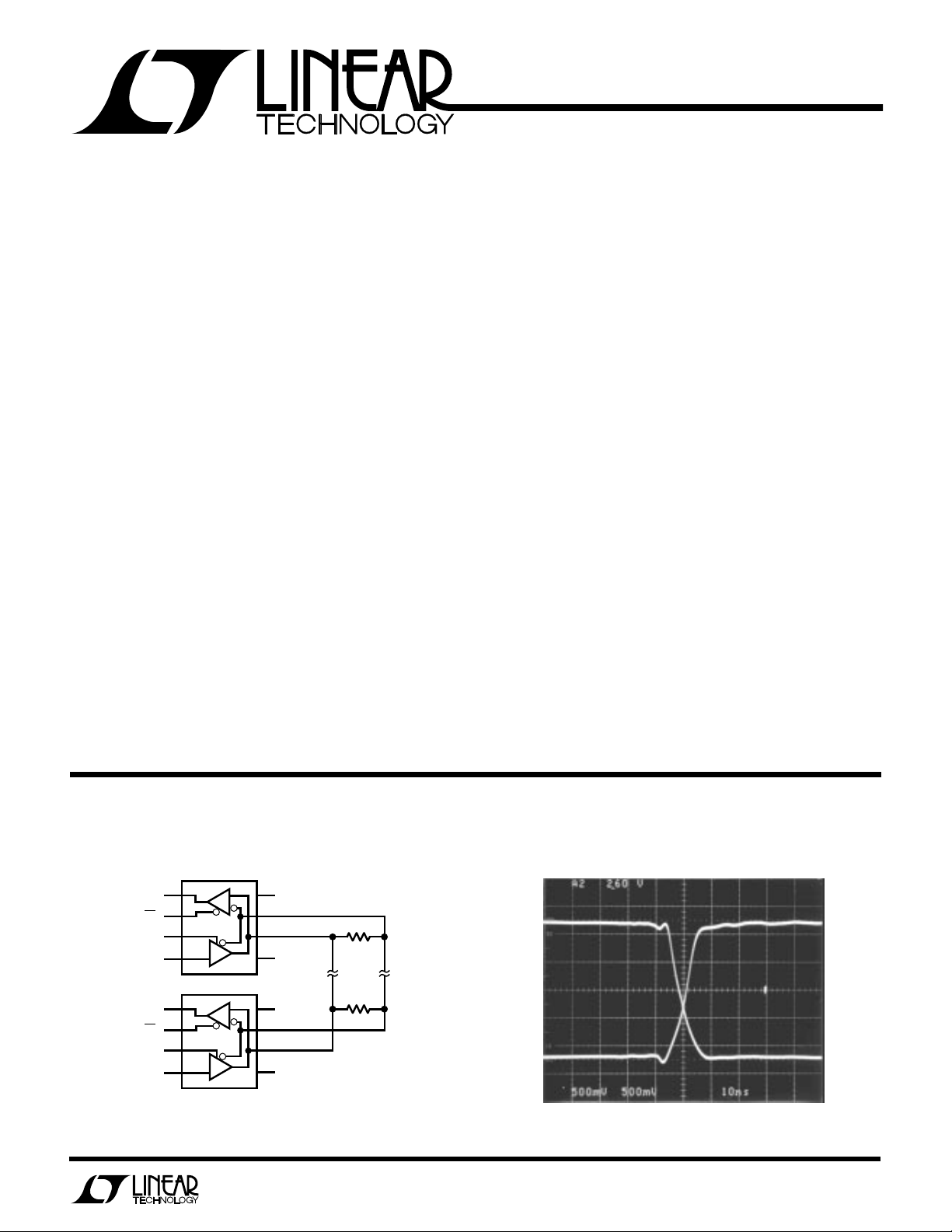
Figure 14. Line Length Test Circuit
Using the test circuit in Figure 14, Figures 15 and 16 show
that with ~20V
common-mode noise injected on the
P-P
line, The LTC485 is able to reconstruct the data stream at
the end of 4000 feet of twisted pair wire.
Figures 17 and 18 show that the LTC485 is able to
comfortably drive 4000 feet of wire at 110kHz.
RO
COMMON-MODE
VOLTAGE (A + B)/2
DI
LTC485 • F17
Figure 17. System Common-Mode Voltage at 110kHz
RO
COMMON-MODE
VOLTAGE (A – B)
RO
COMMON-MODE
VOLTAGE (A + B)/2
DI
LTC485 • F18
Figure 18. System Differential Voltage at 110kHz
DI
When specifying line length vs maximum data rate the
LTC485 • F15
Figure 15. System Common-Mode Voltage at 19.2kHz
RO
DIFFERENTIAL
VOLTAGE A – B
DI
LTC485 • F16
curve in Figure 19 should be used:
Figure 16. System Differential Voltage at 19.2kHz
Figure 19. Cable Length vs Maximum Data Rate
9
Page 10

LTC485
U
TYPICAL APPLICATIO S
Typical RS485 Network
PACKAGE DESCRIPTIO
R
t
R
t
LTC485 • TA03
U
Dimensions in inches (millimeters) unless otherwise noted.
J8 Package
8-Lead Ceramic DIP
0.005
(0.127)
MIN
87
0.405
(10.287)
MAX
65
CORNER LEADS OPTION
(4 PLCS)
0.023 – 0.045
(0.584 – 1.143)
HALF LEAD
0.045 – 0.068
(1.143 – 1.727)
FULL LEAD
OPTION
NOTE: LEAD DIMENSIONS APPLY TO SOLDER DIP OR TIN PLATE LEADS.
OPTION
(7.366 – 8.128)
0.008 – 0.018
(0.203 – 0.457)
0.385 ± 0.025
(9.779 ± 0.635)
0.290 – 0.320
0° – 15°
0.025
(0.635)
RAD TYP
0.045 – 0.068
(1.143 – 1.727)
0.014 – 0.026
(0.360 – 0.660)
12
3
4
0.220 – 0.310
(5.588 – 7.874)
0.015 – 0.060
(0.381 – 1.524)
0.100 ± 0.010
(2.540 ± 0.254)
0.200
(5.080)
MAX
0.125
3.175
MIN
J8 0293
10
Page 11

PACKAGE DESCRIPTIO
U
Dimensions in inches (millimeters) unless otherwise noted.
N8 Package
8-Lead Plastic DIP
0.400
(10.160)
MAX
876
5
LTC485
12
0.300 – 0.320
(7.620 – 8.128)
0.065
(1.651)
0.009 – 0.015
(0.229 – 0.381)
+0.025
0.325
–0.015
+0.635
8.255
()
–0.381
TYP
0.045 ± 0.015
(1.143 ± 0.381)
(2.540 ± 0.254)
0.045 – 0.065
(1.143 – 1.651)
0.100 ± 0.010
3
S8 Package
8-Lead Plastic SOIC
0.250 ± 0.010
(6.350 ± 0.254)
4
0.130 ± 0.005
(3.302 ± 0.127)
0.125
(3.175)
MIN
0.018 ± 0.003
(0.457 ± 0.076)
0.020
(0.508)
MIN
N8 0392
(0.254 – 0.508)
0.008 – 0.010
(0.203 – 0.254)
0.189 – 0.197
(4.801 – 5.004)
7
8
0.228 – 0.244
(5.791 – 6.197)
1
0.010 – 0.020
× 45°
0°– 8° TYP
0.016 – 0.050
0.406 – 1.270
Information furnished by Linear Technology Corporation is believed to be accurate and reliable.
However, no responsibility is assumed for its use. Linear Technology Corporation makes no representation that the interconnection of its circuits as described herein will not infringe on existing patent rights.
0.053 – 0.069
(1.346 – 1.752)
0.014 – 0.019
(0.355 – 0.483)
6
3
2
5
0.150 – 0.157
(3.810 – 3.988)
4
0.004 – 0.010
(0.101 – 0.254)
0.050
(1.270)
BSC
SO8 0392
11
Page 12

LTC485
U.S. Area Sales Offices
NORTHEAST REGION
Linear Technology Corporation
One Oxford Valley
2300 E. Lincoln Hwy.,Suite 306
Langhorne, PA 19047
Phone: (215) 757-8578
FAX: (215) 757-5631
Linear Technology Corporation
266 Lowell St., Suite B-8
Wilmington, MA 01887
Phone: (508) 658-3881
FAX: (508) 658-2701
FRANCE
Linear Technology S.A.R.L.
Immeuble "Le Quartz"
58 Chemin de la Justice
92290 Chatenay Malabry
France
Phone: 33-1-41079555
FAX: 33-1-46314613
GERMANY
Linear Techonolgy GMBH
Untere Hauptstr. 9
D-85386 Eching
Germany
Phone: 49-89-3197410
FAX: 49-89-3194821
SOUTHEAST REGION
Linear Technology Corporation
17060 Dallas Parkway
Suite 208
Dallas, TX 75248
Phone: (214) 733-3071
FAX: (214) 380-5138
CENTRAL REGION
Linear Technology Corporation
Chesapeake Square
229 Mitchell Court, Suite A-25
Addison, IL 60101
Phone: (708) 620-6910
FAX: (708) 620-6977
International Sales Offices
KOREA
Linear Technology Korea Branch
Namsong Building, #505
Itaewon-Dong 260-199
Yongsan-Ku, Seoul
Korea
Phone: 82-2-792-1617
FAX: 82-2-792-1619
SINGAPORE
Linear Technology Pte. Ltd.
101 Boon Keng Road
#02-15 Kallang Ind. Estates
Singapore 1233
Phone: 65-293-5322
FAX: 65-292-0398
SOUTHWEST REGION
Linear Technology Corporation
22141 Ventura Blvd.
Suite 206
Woodland Hills, CA 91364
Phone: (818) 703-0835
FAX: (818) 703-0517
NORTHWEST REGION
Linear Technology Corporation
782 Sycamore Dr.
Milpitas, CA 95035
Phone: (408) 428-2050
FAX: (408) 432-6331
TAIWAN
Linear Technology Corporation
Rm. 801, No. 46, Sec. 2
Chung Shan N. Rd.
Taipei, Taiwan, R.O.C.
Phone: 886-2-521-7575
FAX: 886-2-562-2285
UNITED KINGDOM
Linear Technology (UK) Ltd.
The Coliseum, Riverside Way
Camberley, Surrey GU15 3YL
United Kingdom
Phone: 44-276-677676
FAX: 44-276-64851
JAPAN
Linear Technology KK
5F YZ Bldg.
Iidabashi, Chiyoda-Ku
Tokyo, 102 Japan
Phone: 81-3-3237-7891
FAX: 81-3-3237-8010
Linear Technology Corporation
12
1630 McCarthy Blvd., Milpitas, CA 95035-7487
(408) 432-1900
●
FAX
: (408) 434-0507
●
TELEX
World Headquarters
Linear Technology Corporation
1630 McCarthy Blvd.
Milpitas, CA 95035-7487
Phone: (408) 432-1900
FAX: (408) 434-0507
: 499-3977
06/24/93
LT/GP 0294 5K REV E • PRINTED IN THE USA
LINEAR TECHNOLOGY CORPORATION 1994
 Loading...