

Page 1

LTC4555
SIM Power Supply
and Level Translator
FEATURES
n
SIM Power Supply: 1.8V/3V at 50mA
n
Input Voltage Range: 3V to 6V
n
Controller Voltage Range: 1.2V to 4.4V
n
14kV ESD On All SIM Contact Pins
n
Meets All ETSI, IMT-2000 and ISO7816 SIM/Smart
Card Interface Requirements
n
Level Translators to 1.8V or 3V
n
20μA Operating Current
n
Logic-Controlled Shutdown (ISD < 1μA)
n
Available in a Low Profi le, 16-Pin (3mm × 3mm)
QFN Package
APPLICATIONS
n
SIM Interface in 3G Cellular Telephones
n
Smart Card Readers
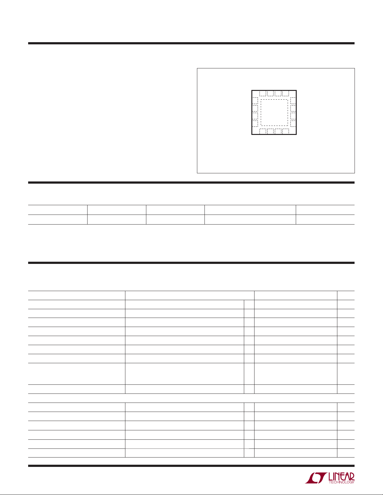
TYPICAL APPLICATION
DESCRIPTION
The LTC®4555 provides power conversion and signal
level shifting needed for low voltage 2.5G and 3G cellular
telephones to interface with 1.8V or 3V subscriber identity
modules (SIMs). The part meets all type approval requirements for 1.8V and 3V SIMs and smart cards. The part
contains an LDO linear regulator to supply SIM power at
either 1.8V or 3V from a 3V to 6V input. The output voltage is selected with a single pin and up to 50mA of load
current can be supplied.
Internal level translators allow controllers operating with
supplies as low as 1.2V to interface with 1.8V or 3V smart
cards. Battery life is maximized by 20μA operating current
and <1μA shutdown current. Board area is minimized by
the 3mm × 3mm leadless QFN package.
L, LT, LTC and LTM are registered trademarks of Linear Technology Corporation.
All other trademarks are the property of their respective owners.
V
CONTROLLER
Typical SIM Interface
V
GND
BAT
(3V TO 6V)
V
BAT
V
CC
RST
CLK
I/0
0.1μF
1μF
SIM/
SMART CARD
INTERFACE
V
CC
RST
CLK
I/0
GND
4555 TA01
4555fb
(1.2V TO 4.4V)
CC
0.1μF
DV
SHDN
V
SEL
R
IN
C
IN
DATA
CC
LTC4555
1
Page 2
LTC4555
PIN CONFIGURATION ABSOLUTE MAXIMUM RATINGS
(Note 1)
V
, DVCC, VCC to GND ............................ –0.3V to 6.5V
BAT
Digital Inputs to GND ................................ –0.3V to 6.5V
CLK, RST, I/O to GND .......................–0.3V to V
Short-Circuit Duration ................................... Infi nite
V
CC
+ 0.3V
CC
Operating Temperature Range (Note 2).... –40°C to 85°C
Junction Temperature ........................................... 125°C
Storage Temperature Range ...................–65°C to 125°C
V
SEL
DV
CC
NC
16-LEAD (3mm s 3mm) PLASTIC QFN
T
JMAX
EXPOSED PAD (PIN 17) IS GND, MUST BE SOLDERED TO PCB
TOP VIEW
DATA
17
NC
RINC
CC
V
I/O
IN
12
NC
CLK
11
GND
10
RST
9
NC
16 15 14 13
1SHDN
2
3
4
5 6 7 8
BAT
V
UD PACKAGE
= 125°C, θJA = 68°C/W, θJC = 4.2°C/W
ORDER INFORMATION
LEAD FREE FINISH TAPE AND REEL PART MARKING PACKAGE DESCRIPTION TEMPERATURE RANGE
LTC4555EUD#PBF LTC4555EUD#TRPBF LAAA
Consult LTC Marketing for parts specifi ed with wider operating temperature ranges.
Consult LTC Marketing for information on non-standard lead based fi nish parts.
For more information on lead free part marking, go to:
For more information on tape and reel specifi cations, go to:
http://www.linear.com/leadfree/
http://www.linear.com/tapeandreel/
16-Lead (3mm × 3mm) Plastic QFN
–40°C to 85°C
ELECTRICAL CHARACTERISTICS
The l denotes the specifi cations which apply over the full operating
temperature range, otherwise specifi cations are at TA = 25°C.
PARAMETER CONDITIONS MIN TYP MAX UNITS
Operating Voltage
V
BAT
Operating Current ICC = 0mA
V
BAT
V
Shutdown Current SHDN = 0V, V
BAT
Operating Voltage
DV
CC
Operating Current f
DV
CC
Shutdown Current SHDN = 0V
DV
CC
Undervoltage Lockout
DV
CC
Output Voltage V
V
CC
V
V
CLK
SEL
SEL
SEL
= 1MHz
= DVCC, V
= DVCC, V
= 0, V
= 4.5V
BAT
= 3V, I
BAT
= 3.3V to 6V, I
BAT
= 2.6V to 6V, I
BAT
= 50mA
VCC
= 0mA to 50mA
VCC
= 0mA to 50mA
VCC
VCC Short-Circuit Current VCC Shorted to GND 60 110 175 mA
Controller Inputs/Outputs
Input Voltage Range SHDN, V
Input Current (I
High Input Threshold Voltage (V
Low Input Threshold Voltage (V
) SHDN, V
IH/IIL
)R
IH
)R
IL
IN
IN
High Input Threshold Voltage (VIH) SHDN, V
Low Input Threshold Voltage (V
) SHDN, V
IL
, RIN, CIN, DATA 0 DV
SEL
, RIN, C
, C
, C
SEL
IN
IN
SEL
SEL
IN
l
l
l
l
l
l
l
36V
20 30 μA
1.2 4.4 V
510μA
0.5 1.1 V
2.8
l
2.8
l
1.7
l
–100 100 nA
l
l
0.2 × DV
l
l
0.4 V
3.0
1.8
0.7 × DV
CC
1μA
1μA
3.2
1.9
CC
CC
1V
4555fb
V
V
V
V
V
V
2
Page 3
LTC4555
ELECTRICAL CHARACTERISTICS
The l denotes the specifi cations which apply over the full operating
temperature range, otherwise specifi cations are at T
PARAMETER CONDITIONS MIN TYP MAX UNITS
High Level Input Current (I
Low Level Input Current (I
High Level Output Voltage (V
Low Level Output Voltage (VOL)DATA I
DATA Pull-Up Resistance Between DATA and DV
SIM Inputs/Outputs (V
High Level Output Voltage (V
Low Level Output Voltage (V
High Level Output Voltage (V
Low Level Output Voltage (V
I/O Pull-Up Resistance Between I/O and V
SIM Inputs/Outputs (V
High Level Output Voltage (V
Low Level Output Voltage (VOL) I/O, IOL = –1mA, DATA = 0V
High Level Output Voltage (V
Low Level Output Voltage (VOL) RST, CLK, IOL = –200μA
I/O Pull-Up Resistance Between I/O and V
SIM Timing Parameters
CLK Rise/Fall Time C
RST, I/O Rise/Fall Time RST, I/O Loaded with 30pF, V
Max CLK Frequency 5MHz
Turn-On Time SHDN = 1, (Note 3) 0.5 ms
V
CC
Discharge Time to 1V SHDN = 0, (Note 3) 0.5 ms
V
CC
)DATA
IH
) DATA
IL
)DATA I
OH
= 3V)
CC
) I/O, IOH = 20μA, DATA = DV
OH
) I/O, IOL = –1mA, DATA = 0V
OL
) RST, CLK, IOH = 20μA
OH
) RST, CLK, IOL = –200μA
OL
= 1.8V)
CC
) I/O, IOH = 20μA, DATA = DV
OH
) RST, CLK, IOH = 20μA
OH
= 30pF, VCC = 1.8V/3V
CLK
= 25°C.
A
= 20μA, I/O = V
OH
= –200μA, I/O = 0V
OL
CC
CC
CC
CC
CC
CC
= 1.8V/3V
CC
l
–20 20 μA
l
l
0.7 × DV
CC
l
13 20 30 kΩ
l
0.8 × V
CC
l
l
0.9 × V
CC
l
6.5 10 14 kΩ
l
0.8 × V
CC
l
l
0.9 × V
CC
l
0.2 × VCC
6.5 10 14 kΩ
l
l
1mA
V
0.4 V
V
0.4 V
V
0.4 V
V
0.3 V
V
V
18 ns
1μs
Note 1: Stresses beyond those listed under Absolute Maximum Ratings
may cause permanent damage to the device. Exposure to any Absolute
Maximum Rating condition for extended periods may affect device
reliability and lifetime.
Note 2: The LTC4555E is guaranteed to meet performance specifi cations
from 0°C to 85°C. Specifi cations over the –40°C to 85°C operating
temperature range are assured by design, characterization and correlation
with statistical process controls.
Note 3: Specifi cation is guaranteed by design and not 100% tested in
production.
4555fb
3
Page 4

LTC4555
TYPICAL PERFORMANCE CHARACTERISTICS
VCC Short-Circuit Current I
170
150
130
110
90
SHORT-CIRCUIT CURRENT (mA)
70
50
–40
–20 0
TEMPERATURE (°C)
40 80 100
20 60
4555 G01
PIN FUNCTIONS
SHDN (Pin 1): Controller Driven Shutdown Pin. This pin
should be high (DV
activate a low current shutdown mode.
(Pin 2): VCC Voltage Select Pin. A low level selects VCC
V
SEL
= 1.8V while driving this pin to DV
(Pin 3): Supply Voltage for the Controller Side I/O
DV
CC
Pins (C
, RIN, DATA). When below 1.1V, the VCC supply
IN
is disabled. This pin should be bypassed with a 0.1μF
ceramic capacitor close to the pin.
NC (Pins 4, 6, 12, 16): No Connect.
(Pin 5): VCC Supply Input. This pin can be between
V
BAT
3V and 6V for normal operation. V
reduces to <1μA in shutdown. This pin should be bypassed
with a 0.1μF ceramic capacitor close to the pin.
(Pin 7): SIM Card VCC Supply. A 1μF low ESR capacitor
V
CC
needs to be connected close to the V
tion. This pin is discharged to GND during shutdown.
) for normal operation and low to
CC
selects VCC = 3V.
CC
quiescent current
BAT
pin for stable opera-
CC
vs V
BAT
BAT
TA = 85°C
3.0 3.5
VCC = 3V
TA = 25°C
TA = 85°C
4.0 5.0
V
BAT
TA = –40°C
TA = –40°C
TA = 25°C
VCC = 1.8V
4.5 5.5 6.0
(V)
4555 G02
(μA)
BAT
I
22
20
18
16
14
12
10
2.5
RST (Pin 9): Reset Output Pin for the SIM Card.
GND (Pin 10): Ground for the SIM and Controller. Proper
grounding and bypassing is required to meet 14kV ESD
specifi cations.
CLK (Pin 11): Clock Output Pin for the SIM Card. This
pin is pulled to ground during shutdown. Fast rising and
falling edges necessitate careful board layout for the CLK
node.
(Pin 13): Clock Input from the Controller.
C
IN
(Pin 14): Reset Input from the Controller.
R
IN
DATA (Pin 15): Controller Side Data I/O. This pin is used
for bidirectional data transfer. The controller output must
be an open-drain confi guration. The open-drain output
must be capable of sinking greater than 1mA.
Exposed Pad (Pin 17): GND. Must be soldered to PCB.
I/O (Pin 8): SIM-Side Data I/O. The SIM card output must
be on an open-drain driver capable of sourcing >1mA.
4
4555fb
Page 5

BLOCK DIAGRAM
PROCESSOR
SHUTDOWN
VOLTAGE
SELECT
LTC4555
V
BAT
(3V TO 6V)
V
CC
C3
0.1μF
PIN
V
SIM
1
2
SHDN
V
SEL
DV
CC
53
V
50mA LDO
BAT
V
CC
C2
0.1μF
7
1.8V/3V
AT 50mA
C1
1μF
PROCESSOR
PROCESSOR
DATA TO/
FROM SIM
CELL PHONE
PROCESSOR
INTERFACE
RESET
FROM
CLOCK
FROM
14
13
15
R
IN
C
IN
20k 10k
DATA
LTC4555
RST
9
CLK
11
I/0
8
GND
10
RESET
CLOCK
BIDIRECTIONAL
I/O
SIM/
SMART CARD
INTERFACE
4555 BD
4555fb
5
Page 6

LTC4555
APPLICATIONS INFORMATION
The LTC4555 provides both regulated power and internal
level translators to allow low voltage controllers to interface
with 1.8V or 3V SIMs or smart cards. The part meets all
ETSI, IMT-2000 and ISO7816 requirements for SIM and
smart card interfaces.
Voltage Regulator
V
CC
The V
regulator with a digitally selected 1.8V or 3V output.
The output voltage is selected via the V
is internally current limited and is capable of surviving an
indefi nite short to GND.
The V
The LTC4555 can use either a low ESR ceramic capacitor
or a tantalum electrolytic capacitor on the V
no special ESR requirements.
V
Level Translators
All SIMs and smart cards contain a clock input, a reset
input and a bidirectional data input/output. The LTC4555
voltage regulator is a 50mA low dropout (LDO)
CC
pin. The output
SEL
output should be bypassed with a 1μF capacitor.
CC
pin, with
CC
should be bypassed with a 0.1μF ceramic capacitor.
BAT
provides level translators to allow controllers to communicate with the SIM. The CLK and RST lines to the
SIM are level shifted from the controller supply (GND to
) to the SIM supply (GND to VCC). The data input to
DV
CC
the SIM requires an open-drain output on the controller.
On-chip pull-up resistors are provided for both the DATA
and I/O lines.
Shutdown Modes
The LTC4555 enters a low current shutdown mode by
pulling the SHDN pin low. The SHDN pin is an active low
input that the controller can use to directly shut down
the part.
ESD Protection
All pins that connect to the SIM/smart card will withstand
14kV of human body model ESD. In order to ensure
proper ESD protection, careful board layout is required.
The GND pin should be tied directly to a GND plane. The
capacitor should be located very close to the VCC pin
V
CC
and tied directly to the GND plane.
6
4555fb
Page 7

PACKAGE DESCRIPTION
LTC4555
UD Package
16-Lead Plastic QFN (3mm × 3mm)
(Reference LTC DWG # 05-08-1691)
0.70 p0.05
3.50 p 0.05
2.10 p 0.05
1.45 p 0.05
(4 SIDES)
PACKAGE OUTLINE
0.25 p0.05
0.50 BSC
RECOMMENDED SOLDER PAD PITCH AND DIMENSIONS
3.00 p 0.10
(4 SIDES)
PIN 1
TOP MARK
(NOTE 6)
NOTE:
1. DRAWING CONFORMS TO JEDEC PACKAGE OUTLINE MO-220 VARIATION (WEED-2)
2. DRAWING NOT TO SCALE
3. ALL DIMENSIONS ARE IN MILLIMETERS
4. DIMENSIONS OF EXPOSED PAD ON BOTTOM OF PACKAGE DO NOT INCLUDE
MOLD FLASH. MOLD FLASH, IF PRESENT, SHALL NOT EXCEED 0.15mm ON ANY SIDE
5. EXPOSED PAD SHALL BE SOLDER PLATED
6. SHADED AREA IS ONLY A REFERENCE FOR PIN 1 LOCATION
ON THE TOP AND BOTTOM OF PACKAGE
0.75 p 0.05
1.45 p 0.10
(4-SIDES)
0.200 REF
0.00 – 0.05
BOTTOM VIEW—EXPOSED PAD
R = 0.115
TYP
15 16
0.50 BSC
PIN 1 NOTCH R = 0.20 TYP
OR 0.25 s 45o CHAMFER
0.40 p 0.10
1
2
(UD16) QFN 0904
0.25 p 0.05
Information furnished by Linear Technology Corporation is believed to be accurate and reliable.
However, no responsibility is assumed for its use. Linear Technology Corporation makes no representation that the interconnection of its circuits as described herein will not infringe on existing patent rights.
4555fb
7
Page 8

LTC4555
RELATED PARTS
PART NUMBER DESCRIPTION COMMENTS
LTC1514 50mA, 650kHz, Step-Up/Down Charge Pump with
Low-Battery Comparator
LTC1515 50mA, 650kHz, Step-Up/Down Charge Pump with
Power-On Reset
LTC1555/LTC1556 650kHz,SIM Power Supply and Level Translator for 3V/5V
SIM Cards
LTC1555L 1MHz, SIM Power Supply and Level Translator for 3V/5V
SIM Cards
LTC1555L-1.8 1MHz, SIM Power Supply and Level Translator for 1.8V/3V/5V
SIM Cards
LTC1755/LTC1756 Smart Card Interface with Serial Control for 3V/5V Smart Card
Applications
LTC1955 Dual Smart Card Interface with Serial Control for 1.8V/3V/5V
Smart Card Applications
LTC1986 900kHz, SIM Power Supply for 3V/5V SIM Cards VIN = 2.6V to 4.4V, V
LTC3250-1.5 250mA,1.5MHz, High Effi ciency Step-Down Charge Pump 85% Effi ciency, VIN = 3.1V to 5.5V, V
LTC3251 500mA,1MHz to 16MHz, Spread Spectrum, Step-Down
Charge Pump
ThinSOT is a trademark of Linear Technology Corporation.
= 2.7V to 10V, V
V
IN
VIN = 2.7V to 10V, V
S8 Package
VIN = 2.7V to 10V, V
SSOP-16, SSOP-20 Packages
= 2.6V to 6.6V, V
V
IN
SSOP-16 Package
VIN = 2.6V to 6.6V, V
SSOP-16
VIN = 2.7V to 7V, V
SSOP-16, SSOP-24
VIN = 3V to 6V, V
QFN-32 Package
ThinSOT™ Package
I
< 1μA, ThinSOT Package
SD
85% Effi ciency, V
I
< 1μA, MS Package
SD
= 3V/5V, IQ = 60μA, ISD = 10μA, S8 Package
OUT
= 3.3V or 5V, IQ = 60μA, ISD < 1μA,
OUT
= 3V/5V, IQ = 60μA, ISD < 1μA,
OUT
= 3V/5V, IQ = 40μA, ISD < 1μA,
OUT
= 1.8V/3V/5V, IQ = 32μA, ISD < 1μA,
OUT
= 3V/5V, IQ = 60μA, ISD < 1μA,
OUT
= 1.8V/3V, IQ = 200μA, ISD < 1μA,
OUT
= 3V/5V, IQ = 14μA, ISD < 1μA,
OUT
= 3.1V to 5.5V, V
IN
= 1.5V, IQ = 35μA,
OUT
= 0.9V to 1.6V, IQ = 9μA,
OUT
8
Linear Technology Corporation
1630 McCarthy Blvd., Milpitas, CA 95035-7417
(408) 432-1900 ● FAX: (408) 434-0507
●
www.linear.com
4555fb
LT 0109 REV B • PRINTED IN USA
© LINEAR TECHNOLOGY CORPORATION 2001
Page 9

 Loading...