

Page 1

LTC4245CUHF
1
DEMO CIRCUIT
985
QUICK START GUIDE
LTC4245CUHF
Multiple Supply Hot Swap Controller
C Compatible Monitoring
with I
2
DESCRIPTION
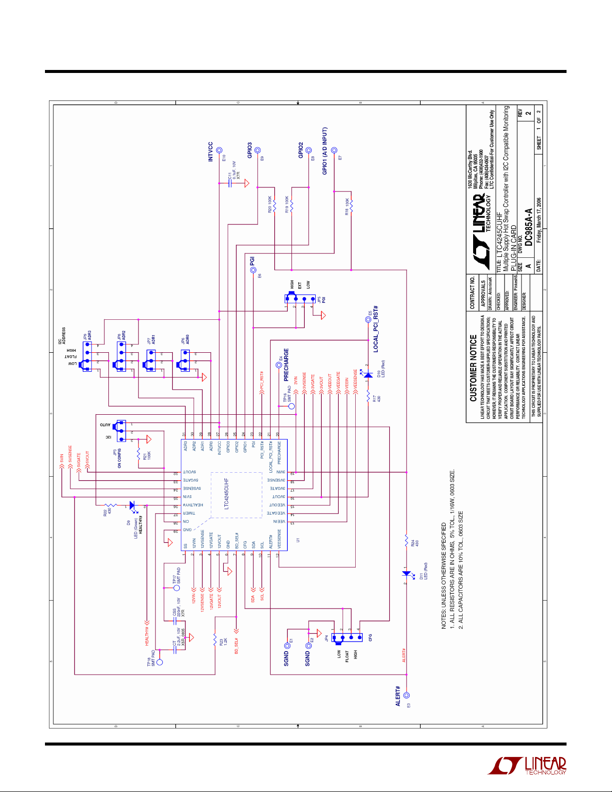
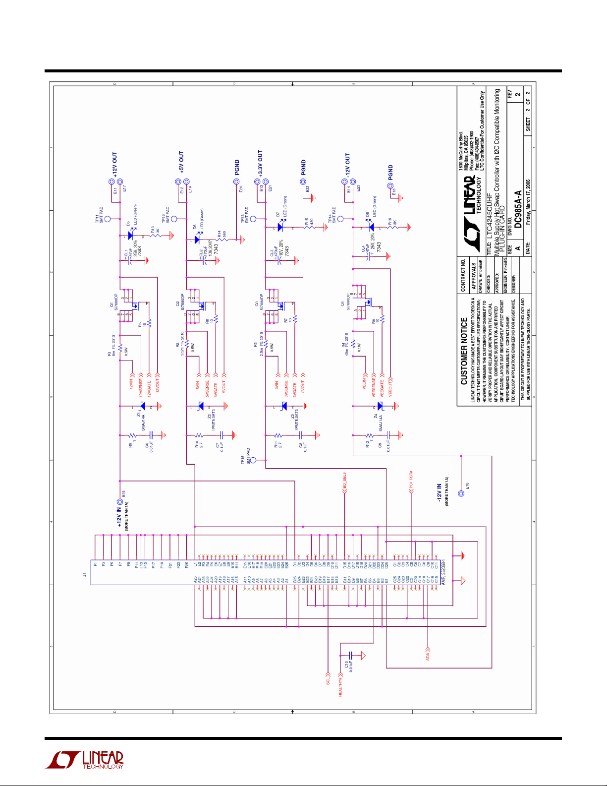
Demonstration circuit 985 showcases
the LTC®4245 Hot Swap™ controller
with I2C™ compatible monitoring in a
CompactPCI™ (CPCI) application. The
LTC4245 resides on the plug-in board,
DC985A-A, which carries a female CPCI
connector. This board plugs into the
male connector on the backplane
board, DC985A-B. The plug-in board
also carries the four n-FET switches
and sense resistors required for hot
swap. LEDs provide visual indication
of the important signals and voltages.
PERFORMANCE SUMMARY
The board can be configured to work
in a PCI Express™ application by adjusting a few jumpers. To access the
powerful monitoring features of the
LTC4245, the I2C port on the backplane board must be connected to a
DC590 board (available separately).
The LTC4245 can then be controlled
with evaluation software running on a
host PC.
Design files for this circuit board
are available. Call the LTC factory.
and LTC are registered trademarks of Linear Technology
Corporation. Hot Swap and QuickEval are trademarks of Linear
Technology Corporation. All other trademarks are the property
of their respective owners.
SYMBOL PARAMETER CONDITIONS MIN TYP MAX UNITS
V
IN
I
OUT,CB
Input Supply Range
+12V IN
+5V IN
+3.3V IN
-12V IN
Circuit Breaker Trip Current
+12V OUT
+5V OUT
+3.3V OUT
-12V OUT
MOSFET Q1-Q4 On, TVS Z1-Z4 Off
CFG Jumper, JP4, at LOW or FLOAT
CFG Jumper, JP4, at HIGH
CFG Jumper, JP4, at LOW
CFG Jumper, JP4, at FLOAT or HIGH
After Start-Up
R1 = 8mΩ, 1%
R2 = 3.5mΩ, 1%
R3 = 2.5mΩ, 1%
R4 = 40mΩ, 1%
10.8
4.5
2.9
2.9
-10.8
0
5.5
6.4
8.9
0.99
12
5
3.3
3.3
-12
6.25
7.1
10
1.25
15
6
6
6
-15
-15
6.9
7.9
11.1
1.52
QUICK START PROCEDURE
1.
Verify that the jumpers are set as
follows:
Backplane board: JP1 BD_SEL#: LOW;
JP2 PCI_RST#: HIGH
Plug-in board: JP3 ON CONFIG: AUTO;
JP5 PGI: HIGH; JP4 CFG: LOW if using all four supplies, FLOAT if using 12V, 5V and 3.3V, HIGH if using
12V, and two 3.3V.
V
V
V
V
V
V
A
A
A
A
Page 2
LTC4245CUHF
2
2.
Mate the plug-in board with the
backplane board.
3.
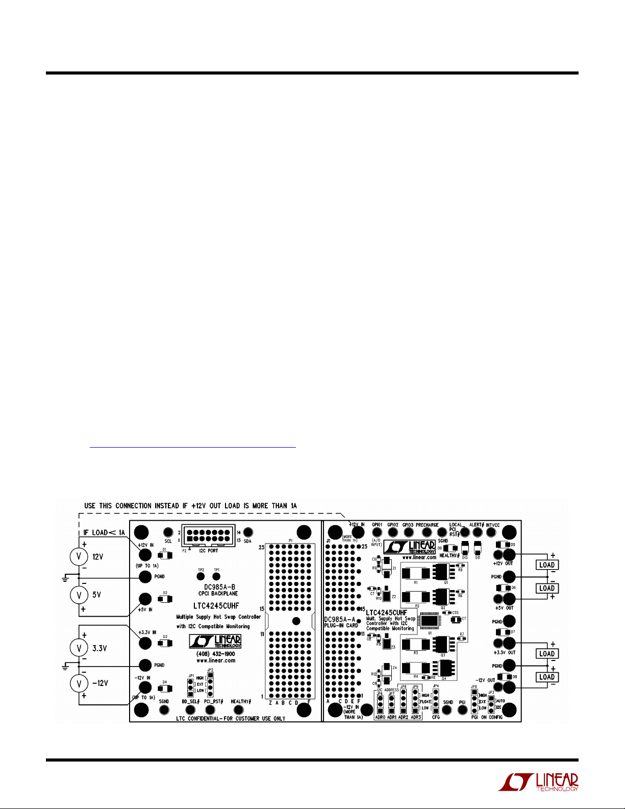
With the power off, connect the input supplies and output loads as
shown in Figure 1. If -12V supply
is not being used, ground -12V IN
and -12V OUT turrets.
4.
Turn on power at the inputs. Check
that the LTC4245 automatically
turns on. LEDs D1 to D4 indicate
when input power is applied, and D5
to D8 show when it is available at
the output. If the output voltages
are within tolerance, HEALTHY#
green LED, D9, turns on, and
LOCAL_PCI_RST# red LED, D10, stays
off. If the outputs remain off,
check the fault registers (Step 8).
5.
To access the ADC data or to control the LTC4245 through I2C, install the QuickEval™ System software on a computer with an available USB port. The download website
is http://www.linear.com/software.
Open the QuickEval software. If already installed, update the software to obtain the LTC4245 driver.
6.
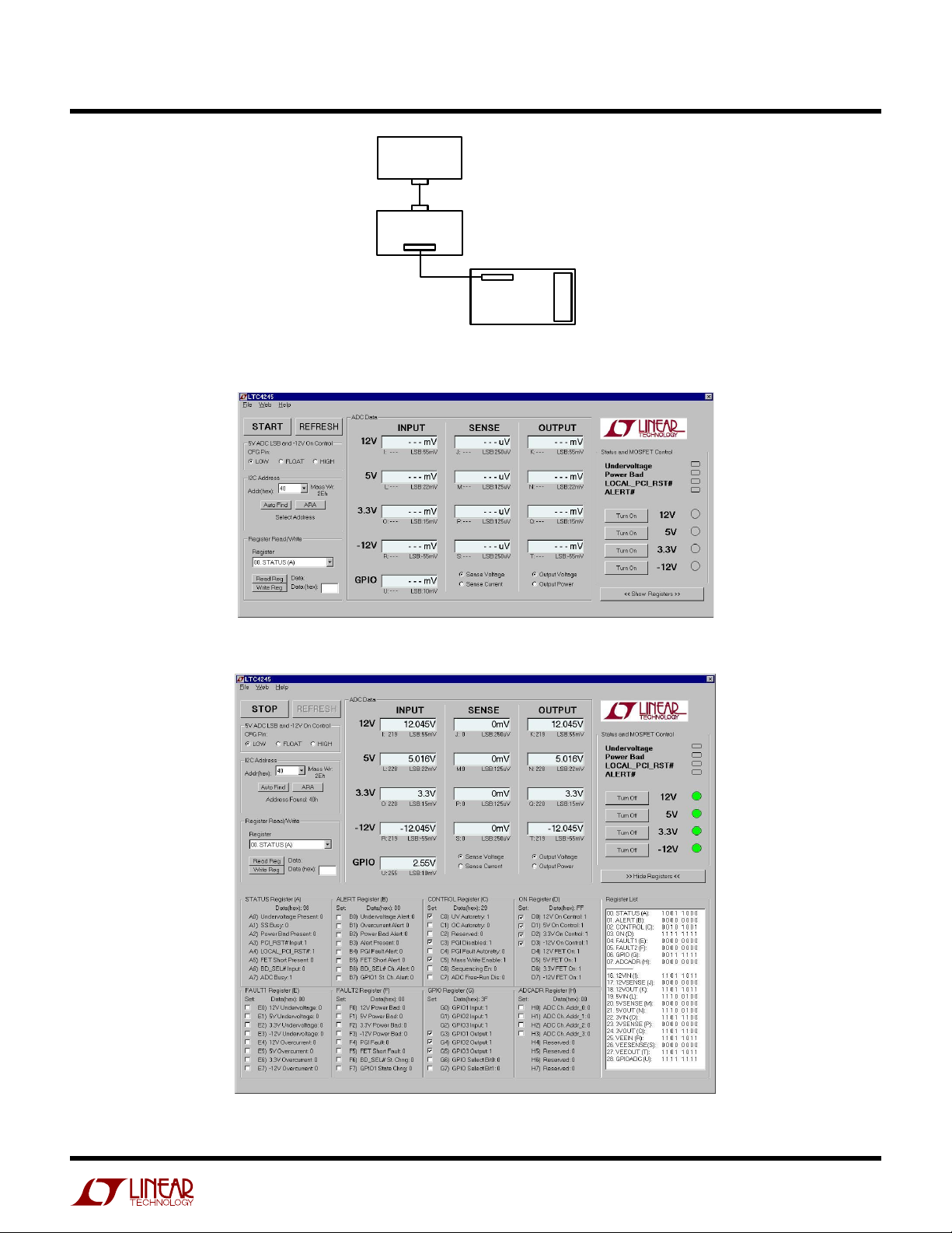
Connect DC590 to the PC with a USB
cable as shown in Figure 2. Connect
the backplane board I2C port, P2,
to the DC590 USB controller board
using the supplied 14-conductor
ribbon cable. Upon connection,
QuickEval will identify the DC985,
and open the LTC4245 interface
software window as shown in Figure
3.
7.
In the software, choose the CFG Pin
option that matches the CFG jumper,
JP4, setting on the board. Click
the Auto Find button in the I2C Address section, so the software can
figure out the I2C slave address of
the LTC4245. After that, click the
START button to get a continuous
update of the LTC4245 internal registers. The software window displays the MOSFET and overall
status.
8.
Click Show Registers button for an
expanded view of all the registers
(Figure 4). The check-boxes can be
used to selectively set or reset
the corresponding register bit.
Figure 1. Proper Measurement Equipment Setup
Page 3
LTC4245CUHF
3
PC
USB
DC590A
14-WIRE
RIBBON
CABLE
Figure 2. QuickEval Setup
Figure 3. Default LTC4245 QuickEval Interface
P2
DC985A-B
P1
Figure 4. LTC4245 QuickEval Interface with Register Display
Page 4

LTC4245CUHF
4
HARDWARE SETUP
BOARD LAYOUT
The top of the plug-in board contains
the core Hot Swap controller and associated components, along with LEDs.
Also on top are various configuration
jumpers and all connection turrets.
The large turrets may be removed to
permit installation of up to 12 gauge
wire for direct, low resistance connections to the board. None of the
turrets are swaged.
The bottom of the boards contains
components for software identification of the board, LED current limiting resistors, the CPCI connector
(J1), and a spare sense resistor.
Also on the bottom is the LTC4245
INTVCC bypass capacitor, C11, and the
supply input and output capacitors.
Except for C11, the other components
are largely unrelated to the core application and are included for the
purposes of the demo board itself.
The spare 50m sense resistor, R1OPT,
can be used to replace the 8m resistor (R1) on the 12V supply to lower
its current limit to CPCI levels.
The boards are designed with two
ground planes, on layers 2 and 3.
Layer 2 is a small signal ground
plane which picks up ground for
LTC4245, the small SGND turrets, C11,
CSS, CT, as well as I2C and configuration jumper related grounding.
Layer 3 is reserved for large signal
grounding, including capacitors on
supply inputs and outputs, large PGND
turrets, input and output LEDs, and
input clamps and snubbers. These two
ground planes join at the CPCI connector ground pins.
HIGHER CURRENT ON ±12V
The CPCI connector pin DC current
should be limited to 1A per pin. The
12V supply has 1 pin; 5V has 2 long
and 6 medium pins; 3.3V has 2 long
and 8 medium pins; -12V has 1 medium
pin. The Si7880DP n-FET used on all
four supplies is rated to 18A at room
temperature.
The circuit breakers for the four
supplies are set as shown in the Performance Summary table. It is dictated by the tolerance on the circuit
breaker trip sense voltage and the
sense resistor.
If the load current on the 12V supply
is more than 1A, the +12V IN turret
on the plug-in card should be used to
supply the input current. Otherwise
the 12V connector pin may be damaged.
To use higher load currents on -12V
OUT use the -12V IN turret on the
plug-in card for the input power supply. The sense resistor R4 will also
need to be replaced with a value
lower than the installed 40m.
PCI EXPRESS APPLICATION
For PCI Express current levels, use
the +12V IN turret on the plug-in
card to supply input power. Set the
CFG pin jumper (JP4) HIGH so a 3.3V
supply can be used at the +5V IN turret. Ground the -12V IN and -12V OUT
turrets. If needed, modify the sense
resistors (R1 to R3) to adjust the
circuit breaker levels.
GPIO1 (A/D INPUT)
The GPIO1 turret is pulled up to 3.3V
with a 100k resistor. It can be used
to measure voltages in a 0V to 2.56V
Page 5

LTC4245CUHF
5
range. The result is displayed in the
ADC Data section of the LTC4245 software window on the computer.
PRECHARGE
As soon as the LTC4245 3VIN pin is
powered up, the PRECHARGE turret can
source up to 70mA at 1V. This is used
in CPCI to pre-bias the bus I/O lines
during insertion. The turret facilitates hooking up the PRECHARGE pin to
external circuitry.
INTVCC
INTVCC was included on the LTC4245 to
allow bypassing of the internal 5.5V
supply rail for superior noise immunity. It is also permissible to steal
a small current of up to 3mA off the
INTVCC pin to bias address pins or
ancillary circuits. A turret is provided for connections to INTVCC.
CONNECTORS
SDA and SCL can be connected directly
to an I2C bus.
JUMPERS
JP1 BD_SEL#: Connects BD_SEL# back-
plane signal either to ground or
leaves it floating, whereby it will
be pulled up by the 1.2k on the
plug-in card to 5V. In the latter
case, the BD_SEL# turret can be connected to external insertion-detect
logic to initiate turn-on of LTC4245.
Removing and reinstalling the shunt
at LOW will cycle power to the board
and also reset the LTC4245 fault registers.
JP2 PCI_RST#: Sets the backplane reset signal PCI_RST# high, low or
floating. When floating, the PCI_RST#
turret should be driven with an external signal. This jumper will affect the LOCAL_PCI_RST# output of the
LTC4245 (LED D10).
J1: Plug-in card female CompactPCI
connector. This connector mates with
the P1 connector on the backplane
board to allow power and control signals to flow to the LTC4245 and the
supply outputs. The connector utilizes guiding features to ensure correct polarized mating.
P1: Backplane card male CompactPCI
connector. There are three lengths of
pins on this connector. Long 5V, 3.3V
and GND pins provide early power to
the LTC4245. Majority of the pins are
medium length. The short BD_SEL# pin
mates last, and provides the turn-on
signal to the LTC4245.
P2 I2C PORT: Connector for DC590 I2C
adapter card. This card converts a
computer’s USB port to I2C. If P2 is
not connected, the turret terminals
JP3 ON CONFIG: At start-up the
LTC4245 operates in one of two modes:
in AUTO mode it turns on when BD_SEL#
goes low; in I2C mode it waits for an
I2C turn-on command, even after
BD_SEL# goes low, to turn-on the
switches.
JP4 CFG: Sets the CFG pin high, low
or floating. This affects the input
supply range requirement for FET
turn-on. For a CPCI application requiring all four supplies, set it
low. Refer the Performance Summary
table and the datasheet for more details.
JP5 PGI: Sets the PGI pin of the
LTC4245 high, low or floating. When
floating, the PGI turret should be
driven with an external signal, such
as the RESET# output of an external
supply monitor. Setting the PGI pin
Page 6

LTC4245CUHF
6
low can lead to a PGI fault causing
all FETs to be turned off.
JP6 to JP9 ADR0 to ADR3: Selects 1 of
32 possible addresses for the LTC4245
I2C interface by strapping the address pins high, low or allowing them
to float. An address table is shown
in the datasheet and the Help menu of
the evaluation software. The software
can automatically scan and identify
the I2C address, regardless of the
pin setting.
LEDs
D1 to D8: D1 to D4 indicate if the
input supplies are high. D5 to D8
light up when the supply outputs
power up, after the FET switches turn
on.
D9 HEALTHY#: This should light up at
the end of the start-up timing cycle
after all the supply outputs power
up. It will turn off as soon as any
FET switch is turned off or if any
output falls out of tolerance.
D10 LOCAL_PCI_RST#: This LED normally
flashes briefly during start-up and
power-down. This is because it is
powered off +3.3V OUT and the pin is
released at the end of the start-up
timing cycle. It will be lit continuously if +3.3V OUT is high and
PCI_RST# is set low with JP2.
D11 ALERT#: The ALERT# pin pulls low
and turns on this LED if a fault occurs and that fault’s alert is enabled in the ALERT register. The
alert can be cleared either by resetting bit B3 in the ALERT register or
writing to the LTC4245 alert response
address (ARA).
SOFTWARE SETUP
Communicating with the LTC4245 I2C
interface requires the QuickEval System software and a DC590 board. The
QuickEval software is available from
the website www.linear.com/software.
The QuickEval software talks to the
DC590 board through the USB port of
the PC. The DC590 is connected to the
I2C port (P2) on the DC985A-B with
the supplied 14-wire ribbon cable
(Figure 2). When connected, the
QuickEval software identifies the
DC985 and brings up the LTC4245 interface as shown in Figure 3. When
experiencing problems with the software, try unplugging and plugging the
DC590 board from the PC. Also refer
the DC590 Quick Start guide.
I2C ADDRESS SELECTION
Select in the drop down list box the
Write address byte of the LTC4245
that is to be communicated with. The
address pins to I2C address map can
be found in the Help menu. Easier
still, the Auto Find button will scan
through the 32 individual LTC4245 addresses and list which addresses responded with an acknowledge. If multiple LTC4245s are on the bus lines,
the Mass Write address 2Eh can be selected to write to all LTC4245s at
the same time. The ARA button sends
the Alert Response protocol address
and displays the address of the device holding its ALERT# pin low.
5V ADC LSB AND -12V ON CONTROL
Select the radio button that corresponds with the CFG pin jumper, JP4,
Page 7

LTC4245CUHF
7
setting on the plug-in board. Refer
to Table 1 for the effect of this
setting on software parameters.
CFG PIN 5VIN LSB 5VOUT LSB
LOW 22mV 22mV D3
FLOAT 22mV
HIGH 15mV 15mV D0
Table 1: CFG Pin Setting
START AND REFRESH BUTTONS
Click on the START button to enable a
timer that continuously updates the
interface with the latest data from
the LTC4245. This button will display
STOP when the timer is enabled. Click
on STOP to stop the timer. Click on
REFRESH for a single update.
ADC DATA DISPLAY
The data read from the LTC4245 ADC
registers I to U is displayed in an
easy to read format by multiplying
the data with the LSB size and displaying it as a voltage. The current
sense values can be displayed as either a voltage drop (default) or a
current. The sense resistance values
cannot be edited while the software
is in polling mode. There is also an
option for displaying output power
instead of output voltage.
REGISTER DISPLAY OPTIONS
The bits of registers A to H are
shown in detail by clicking on the
Show Registers button (Figure 4).
Checking a box to the left of each
bit of the Read/Write registers sets
the respective bit, while unchecking
a box clears the bit. The bit status
is shown to the right of each bit after every refresh of the interface.
In the Register List box a bit map of
22mV D0
-12V ON/OFF
CONTROL BIT
all the registers is shown and is updated with each refresh of the interface.
The Register Read/Write section allows for the user to enter and write
data to a particular register. Select
the register to be written to in the
drop down menu. Enter the data in hex
and click on Write to send the data,
and then click Read to verify the
write. Read data is displayed both in
hex and decimal.
MOSFET STATUS AND CONTROL
The MOSFET status is shown with a
display, which is colored:
■
Green, when the FET On Status bit
(D4 to D7) is high; the FET control
button will read “Turn Off”
■
Clear, if FET On Status bit is low
and the corresponding FET On control bit (D0 to D3) is also low;
the FET button will read “Turn On”
■
Red, if FET On Status bit is low
and the corresponding FET On control bit is also high; the FET control button will read “Clear Fault”
The “Turn On” control button sets the
corresponding supply’s FET On control
bit high, while “Turn Off” clears it
to logic low. As mentioned before, if
CFG pin radio button is set to FLOAT
or HIGH, the -12V MOSFET is controlled with the 12V FET On control
bit, D0, instead of D3. “Clear Fault”
button writes zeros to the FAULT1 and
FAULT2 registers, in an attempt to
turn-on the MOSFETs by clearing fault
bits. If a fault is still present,
then that fault bit will be set again
by the LTC4245, thus preventing turnon.
Page 8
LTC4245CUHF
8
Page 9
LTC4245CUHF
9
Page 10

LTC4245CUHF
10
Page 11

Mouser Electronics
Authorized Distributor
Click to View Pricing, Inventory, Delivery & Lifecycle Information:
Analog Devices Inc.:
DC985A-A/B
 Loading...