

Page 1
LTC4100
Smart Battery
Charger Controller
FEATURES
n
Single Chip Smart Battery Charger Controller
n
100% Compliant (Rev. 1.1) SMBus Support Allows
for Operation with or without Host
n
SMBus Accelerator Improves SMBus Timing
n
Wide Output Voltage Range: 3.5V to 26V
n
Hardware Interrupt and SMBAlert Response
Eliminate Interrupt Polling
n
High Effi ciency Synchronous Buck Charger
n
0.5V Dropout Voltage; Maximum Duty Cycle > 98%
n
AC Adapter Current Limit Maximizes Charge Rate
n
±0.8% Voltage Accuracy; ±4% Current Accuracy
n
Up to 4A Charging Current Capability
n
10-Bit DAC for Charge Current Programming
n
11-Bit DAC for Charger Voltage Programming
n
User-Selectable Overvoltage and Overcurrent Limits
n
High Noise Immunity SafetySignal Sensor
n
Available in a 24-Pin SSOP Package
APPLICATIONS
n
Portable Instruments and Computers
n
Data Storage Systems and Battery Backup Servers
L, LT, LTC, LTM, Linear Technology and the Linear logo are registered trademarks of Linear
Technology Corporation. All other trademarks are the property of their respective owners.
Protected by U.S. Patents including 6650174 and 5723970.
DESCRIPTION
The LTC®4100 Smart Battery Charger is a single chip
charging solution that dramatically simplifi es construction
of an SBS compliant system. The LTC4100 implements
a Level 2 charger function whereby the charger can be
programmed by the battery or by the host. A SafetySignal
on the battery being charged is monitored for temperature,
connectivity and battery type information. The SMBus
interface remains alive when the AC power adapter is
removed and responds to all SMBus activity directed to
it, including SafetySignal status (via the ChargerStatus
command). The charger also provides an interrupt to the
host whenever a status change is detected (e.g., battery
removal, AC adapter connection).
Charging current and voltage are restricted to chemistryspecifi c limits for improved system safety and reliability.
Limits are programmable by two external resistors. Additionally, the maximum average current from the AC
adapter is programmable to avoid overloading the adapter
when simultaneously supplying load current and charging
current. When supplying system load current, charging current is automatically reduced to prevent adapter
overload.
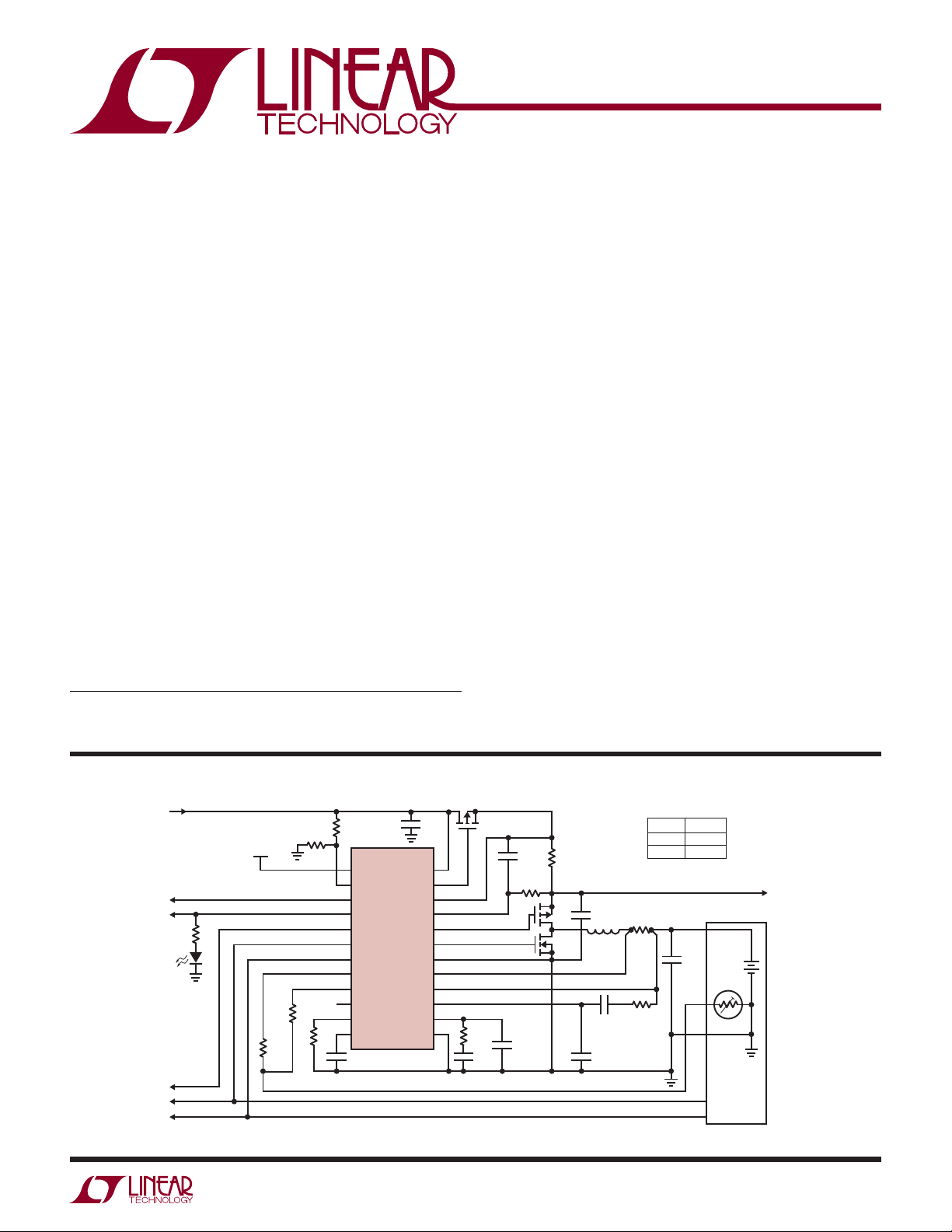
TYPICAL APPLICATION
DCIN
1.21k
1.13k
54.9k
CHGEN
ACP
SMBALERT#
SMBCLK
SMBDAT
3V
TO 5.5V
10k
LTC4100
DCIN
INFET
CLP
CLN
TGATE
BGATE
PGND
CSP
BAT
V
GND
SET
I
0.1µF
TH
5
4
24
23
1
3
2
21
22
18
19
12
6.04k
0.12µF
SafetySignal
0.1µF
0.0015µF
13.7k
17
11
6
10
7
9
8
15
16
13
14
20
0.068µF
V
DD
DCDIV
CHGEN
ACP
SMBALERT
SCL
SDA
THB
THA
I
LIM
V
LIM
I
DC
Figure 1. 4A Smart Battery Charger
V
PART
BAT
< 5.5V
LTC4101
> 5.5V
0.033
5k
20µF
0.025
10µH
100
0.01µF
0.1µF
LTC4100
SMART BATTERY
20µF
SMBCLK
SMBDAT
SYSTEM LOAD
4100 TA01
4100fb
1
Page 2
LTC4100
(Note 1)
Voltage from VDD to GND ................................. 7V/–0.3V
Voltage from CHGEN, DCDIV, SDA,
SCL and SMBALERT to GND ............................ 7V/–0.3V
Voltage from DCIN, CLP, CLN to GND ............ 32V/–0.3V
Voltage from CLP to CLN .......................................±0.3V
PGND wrt. GND .................................................... ±0.3V
CSP, BAT to GND ............................................... 28V/–5V
Operating Ambient Temperature Range (Note 4)
.................................................................– 40°C to 85°C
Junction Temperature Range ................ –40°C to 125°C
Storage Temperature Range ..................–65°C to 150°C
Lead Temperature (Soldering, 10 sec)...................300°C
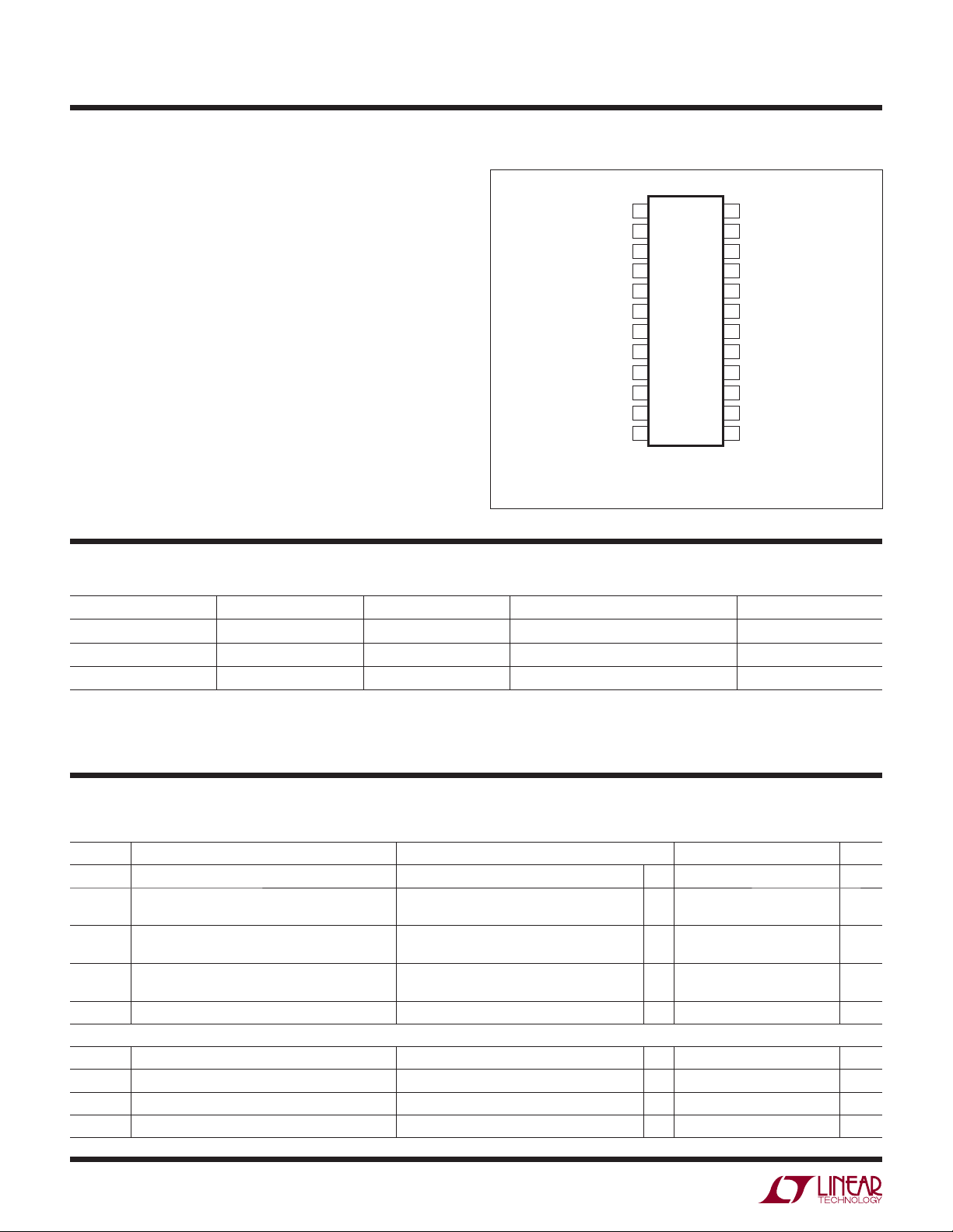
PIN CONFIGURATION ABSOLUTE MAXIMUM RATINGS
TOP VIEW
TGATE
PGND
BGATE
INFET
DCIN
CHGEN
SMBALERT
SDA
SCL
ACP
DCDIV
GND
1
2
3
4
5
6
7
8
9
10
11
12
G PACKAGE
24-LEAD PLASTIC SSOP
T
= 125°C, θJA = 90°C/W
JMAX
CLP
24
CLN
23
BAT
22
CSP
21
I
20
DC
I
19
TH
V
18
SET
V
17
DD
THA
16
THB
15
V
14
LIM
I
13
LIM
ORDER INFORMATION
LEAD FREE FINISH TAPE AND REEL PART MARKING PACKAGE DESCRIPTION TEMPERATURE RANGE
LTC4100EG#PBF LTC4100EG#TRPBF LTC4100EG 24-Lead Plastic SSOP –40°C to 85°C
LEAD BASED FINISH TAPE AND REEL PART MARKING PACKAGE DESCRIPTION TEMPERATURE RANGE
LTC4100EG LTC4100EG#TR LTC4100EG 24-Lead Plastic SSOP –40°C to 85°C
Consult LTC Marketing for parts specifi ed with wider operating temperature ranges.
For more information on lead free part marking, go to:
For more information on tape and reel specifi cations, go to:
ELECTRICAL CHARACTERISTICS
The l denotes the specifi cations which apply over the full operating
temperature range, otherwise specifi cations are at TA = 25°C. V
SYMBOL PARAMETER CONDITIONS MIN TYP MAX UNITS
DCIN Operating Range
I
DCIN
V
TOL
I
TOL
V
DD
Shutdown
UVLO Undervoltage Lockout Threshold DCIN Rising, V
DCIN Operating Current Charging, Sum of Currents on DCIN,
Charge Voltage Accuracy (Note 2)
Charge Current Accuracy (Note 3) V
VDD Operating Voltage 0V ≤ V
Battery Leakage Current DCIN = 0V, V
Power-Fail Part Held in Reset Until this VDD Present
V
DD
DCIN Current in Shutdown V
http://www.linear.com/leadfree/
http://www.linear.com/tapeandreel/
= 20V, VDD = 3.3V, V
DCIN
CLP and CLN
– V
CSP
I
DAC
CHGEN
Target = 102.3mV
BAT
= 0xFFFF ●
≤ 28V
DCIN
= V
CLP
CLN
= 0V
BAT
= 0V 2 3 mA
= V
CSP
= V
= 12V unless otherwise noted. (Note 4)
BAT
628V
●
35 mA
–0.8
–1
●
–4
45%
–5
3 5.5 V
●
BAT
●
4.2 4.7 5.5 V
●
●
15 35 µA
0.8
1
%
%
%
3V
4100fb
2
Page 3

LTC4100
ELECTRICAL CHARACTERISTICS
The l denotes the specifi cations which apply over the full operating
temperature range, otherwise specifi cations are at T
= 25°C. V
A
SYMBOL PARAMETER CONDITIONS MIN TYP MAX UNITS
Current Sense Amplifi er, CA1
Input Bias Current into BAT Pin 11.66 µA
CMSL CA1/I
CMSH CA1/I
Current Comparators I
I
TMAX
I
TREV
Input Common Mode Low
1
Input Common Mode High V
1
and I
CMP
REV
Maximum Current Sense Threshold (V
Reverse Current Threshold (V
CSP–VBAT
DCIN
)V
CSP–VBAT
ITH
= 2.5V
)–30mV
Current Sense Amplifi er, CA2
Transconductance 1 mmho
Source Current Measured at I
Sink Current Measured at I
Current Limit Amplifi er
Transconductance 1.5 mmho
V
I
CLP
CLN
Current Limit Threshold
CLN Input Bias Current 100 nA
Voltage Error Amplifi er, EA
Transconductance 1 mmho
Sink Current Measured at I
OVSD Overvoltage Shutdown Threshold as a Percent of
Programmed Charger Voltage
Input P-Channel FET Driver (INFET)
DCIN Detection Threshold (V
DCIN–VCLP
Forward Regulation Voltage (V
Reverse Voltage Turn-Off Voltage (V
INFET ON Clamping Voltage (V
INFET OFF Clamping Voltage (V
) DCIN Voltage Ramping Up from V
DCIN–VCLP
DCIN–VINFET
DCIN–VINFET
)
DCIN–VCLP
)I
)I
)
= 1µA
INFET
= –25µA 0.25 V
INFET
Oscillator
f
OSC
f
MIN
DC
MAX
Regulator Switching Frequency 255 300 345 kHz
Regulator Switching Frequency in Drop Out Duty Cycle ≥ 98% 20 25 kHz
Regulator Maximum Duty Cycle V
CSP
= V
Gate Drivers (TGATE, BGATE)
TGTR
TGTF
High (V
V
TGATE
V
BGATE
V
TGATE
V
BGATE
CLP-VTGATE
High C
Low (V
CLP-VTGATE
Low I
TGATE Transition Time
TGATE Rise Time
TGATE Fall Time
)I
)C
TGATE
LOAD
LOAD
BGATE
C
LOAD
C
LOAD
BGATE Transition Time
BGTR
BGTF
BGATE Rise Time
BGATE Fall Time
at Shutdown (V
V
TGATE
at Shutdown I
V
BGATE
CLN-VTGATE
)I
C
LOAD
C
LOAD
TGATE
TGATE
= 20V, VDD = 3.3V, V
DCIN
≤ 28V
, V
TH
, V
TH
TH, VITH
BAT
= 1.4V –40 µA
ITH
= 1.4V 40 µA
ITH
= 1.4V 36 µA
= 12V unless otherwise noted. (Note 4)
BAT
0V
●
●
140 165 200 mV
●
93 100 107 mV
●
102 107 110 %
●
CLP
–0.05V
0 0.17 0.25 V
●
●
–60 –25 mV
●
55.86.5 V
●
25 50 mV
98 99 %
V
–0.2 V
CLN
= –1mA 50 mV
= 3000pF 4.5 5.6 10 V
= 3000pF 4.5 5.6 10 V
= 1mA 50 mV
= 3000pF, 10% to 90%
= 3000pF, 10% to 90%
= 3000pF, 10% to 90%
= 3000pF, 10% to 90%
50
50
40
40
110
100
90
80
= –1µA 100 mV
= 1µA 100 mV
4100fb
ns
ns
ns
ns
3
Page 4
LTC4100
ELECTRICAL CHARACTERISTICS
The l denotes the specifi cations which apply over the full operating
temperature range, otherwise specifi cations are at T
= 25°C. V
A
SYMBOL PARAMETER CONDITIONS MIN TYP MAX UNITS
AC Present Comparator
V
ACP
DCDIV Threshold V
DCDIV
DCDIV Hysteresis 25 mV
DCDIV Input Bias Current V
ACP V
OH
ACP V
OL
DCDIV to ACP Delay V
DCDIV
I
= –2mA 2 V
ACP
I
= 1mA 0.5 V
ACP
DCDIV
SafetySignal Decoder
SafetySignal Trip (RES_COLD/RES_OR) R
SafetySignal Trip (RES_IDEAL/RES_COLD) R
SafetySignal Trip (RES_HOT/RES_IDEAL) R
SafetySignal Trip (RES_UR/RES_HOT) R
= 1130 ±1%, C
THA
R
= 54.9 ±1%
THB
= 1130 ±1%, C
THA
R
= 54.9 ±1%
THB
= 1130 ±1%, C
THA
R
= 54.9 ±1%
THB
= 1130 ±1%, C
THA
R
= 54.9 ±1%
THB
Time Between SafetySignal Measurements DCDIV = 1.3V
DCDIV = 1V
DACs
Charging Current Resolution Guaranteed Monotonic Above I
Charging Current Granularity R
Wake-Up Charging Current (I
) All Values of R
WAKE-UP
= 0
ILIM
R
= 10k ±1%
ILIM
R
= 33k ±1%
ILIM
R
= Open (or Short to VDD)
ILIM
All Values of R
Charging Current Limit
CSP – BAT
R
ILIM =
Charging Current = 0x03FF (0x0400 Note 7)
R
ILIM =
Charging Current = 0x07FE (0x0800 Note 7)
R
ILIM =
Charging Current = 0x0BFC (0x0C00 Note 7)
R
ILIM =
Charging Current = 0x0FFC (0x1000 Note 7)
Charging Voltage Resolution Guaranteed Monotonic (2.9V ≤ V
Charging Voltage Granularity 16 mV
Charging Voltage Limit R
VLIM
Charging Voltage = 0x2260 (Note 7)
R
VLIM
Charging Voltage = 0x3330 (Note 7)
R
VLIM
Charging Voltage = 0x4400 (Note 7)
R
VLIM
Charging Voltage = 0x5400 DCIN ≥ 22V
(Note 7)
R
VLIM
Charging Voltage = 0x6D60 DCIN ≥ 29V
(Note 7)
= 20V, VDD = 3.3V, V
DCIN
Rising from 1V to 1.4V
= 12V unless otherwise noted. (Note 4)
BAT
1.14 1.20 1.26 V
●
= 1.2V –1 1 µA
= 1.3V 10 µs
= 1nF (Note 6)
TH
= 1nF (Note 6)
TH
= 1nF (Note 6)
TH
= 1nF (Note 6)
TH
95 100 105 k
●
28.5 30 31.5 k
●
2.85 3 3.15 k
●
425 500 575
●
32
250
/16 10 Bits
MAX
1
2
4
4
ILIM
VLIM
0 (0-1A)
10k ±1% (0-2A)
33k ±1% (0-3A)
0pen (or Short to VDD) (0-4A)
= 0
= 10k ±1%
= 33k ±1%
= 100k ±1%
= 0pen (or Short to VDD)
28V) 11 Bits
BAT ≤
80 (Note 5) mA
97.3 107.3 mV
97.3 107.3 mV
72.3 82.3 mV
97.3 107.3 mV
8.730 8.800 8.870 V
12.999 13.104 13.209 V
17.269 17.408 17.547 V
21.538 21.712 21.886 V
27.781 28.006 28.231 V
4100fb
ms
ms
mA
mA
mA
mA
4
Page 5

LTC4100
ELECTRICAL CHARACTERISTICS
The l denotes the specifi cations which apply over the full operating
temperature range, otherwise specifi cations are at T
= 25°C. V
A
SYMBOL PARAMETER CONDITIONS MIN TYP MAX UNITS
Logic Levels
V
IL
V
IH
V
OL
I
IL
I
IH
V
OL
I
LEAK
V
OL
V
IL
V
IH
SCL/SDA Input Low Voltage VDD = 3V and VDD = 5.5V
SCL/SDA Input High Voltage VDD = 3V and VDD = 5.5V
SDA Output Low Voltage I
SCL/SDA Input Current V
SCL/SDA Input Current V
SMBALERT Output Low Voltage I
SMBALERT Output Pull-Up Current V
SDA/SCL/SMBALERT Power Down Leakage V
PULL-UP
, V
SDA
, V
SDA
PULL-UP
SMBALERT
, V
SDA
CHGEN Output Low Voltage IOL = 100µA
CHGEN Output Pull-Up Current V
CHGEN
CHGEN Input Low Voltage
CHGEN Input High Voltage VDD = 3V
V
= 5.5V
DD
Power-On Reset Duration V
Ramp from 0V to >3V in <5µs 100 µs
DD
SMBus Timing (Refer to System Management Bus Specifi cation, Revision 1.1, Section 2.1 for Timing Diagrams)
t
HIGH
t
LOW
t
R
t
F
t
SU:STA
t
HD:STA
t
HD:DAT
SCL Serial Clock High Period I
SCL Serial Clock Low Period I
SDA/SCL Rise Time C
SDA/SCL Fall Time C
PULL-UP
R
= 9.31k, VDD = 3V and VDD = 5.5V
PU
PULL-UP
R
= 9.31k, VDD = 3V and VDD = 5.5V
PU
LOAD
V
= 5.5V
DD
LOAD
V
= 5.5V
DD
Start Condition Setup Time VDD = 3V and VDD = 5.5V
Start Condition Hold Time VDD = 3V and VDD = 5.5V
SDA to SCL Falling-Edge Hold Time, Slave
VDD = 3V and VDD = 5.5V
Clocking in Data
t
TIMEOUT
Time Between Receiving Valid ChargingCurrent()
VDD = 3V and VDD = 5.5V
and ChargingVoltage() Commands
= 20V, VDD = 3.3V, V
DCIN
BAT
= 350µA
= V
SCL
IL
= V
SCL
IH
= 500µA
= V
OL
, V
SCL
SMBALERT
= V
OL
= 350µA, C
= 350µA, C
= 5.5V, VDD = OV
= 250pF,
LOAD
= 250pF,
LOAD
= 250pF, RPU = 9.31k, VDD = 3V and
= 250pF, RPU = 9.31k, VDD = 3V and
= 12V unless otherwise noted. (Note 4)
●
2.1 V
●
●
–1 1 µA
–1 1 µA
●
–17.5 –10 –3.5 µA
–2 2 µA
●
●
–17.5 –10 –3.5 µA
●
2.5
●
3.9
4µs
●
4.7 15000 µs
●
●
●
4.7 µs
●
4µs
●
300 ns
●
140 175 210 sec
●
0.8 V
0.4 V
0.4 V
0.5 V
0.9 V
1000 ns
300 ns
V
V
Note 1: Stresses beyond those listed under Absolute Maximum Ratings
may cause permanent damage to the device. Exposure to any Absolute
Maximum Rating condition for extended periods may affect device
reliability and lifetime.
Note 2: See Test Circuit.
Note 3: Does not include tolerance of current sense resistor.
Note 4: The LTC4100E is guaranteed to meet performance specifi cations
from 0°C to 70°C. Specifi cations over the –40°C to 85°C operating
temperature range are assured by design, characterization and correlation
with statistical process controls.
Note 5: Current accuracy dependent upon circuit compensation and sense
resistor.
Note 6: C
is defi ned as the sum of capacitance on THA, THB and
TH
SafetySignal.
Note 7: The corresponding overrange bit will be set when a HEX value
greater than or equal to this value is used.
4100fb
5
Page 6
LTC4100
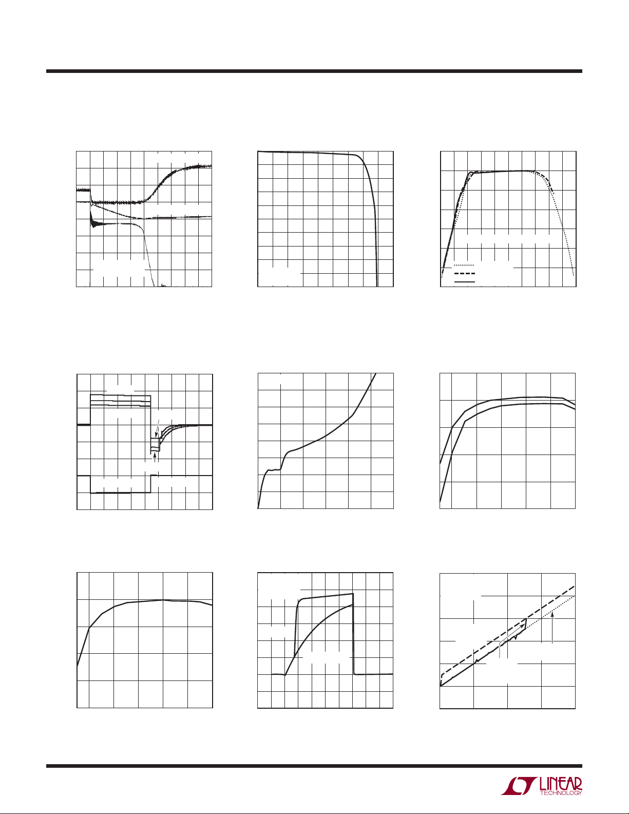
TYPICAL PERFORMANCE CHARACTERISTICS
INFET Response Time to
Reverse Current V
= 0
V
gs
V
= 0V
s
Id (REVERSE) OF
PFET (5A/DIV)
I
= 0A
d
TEST PERFORMED ON DEMOBOARD
= 15VDC
V
IN
CHARGER = ON
= <10mA
I
CHARGE
Vgs OF PFET (2V/DIV)
Vs OF PFET (5V/DIV)
1.25µs/DIV
V
= 12.6V
CHARGE
INFET = 1/2 Si4925DY
4100 G01
–0.5
–1.0
–1.5
–2.0
–2.5
–3.0
–3.5
–4.0
OUTPUT VOLTAGE ERROR (%)
–4.5
–5.0
vs I
OUT
BAT
= 12.6V
OUT
OUTPUT CURRENT (A)
0
DCIN = 20V
V
0 0.5 1.0 2.0 3.0 4.01.5 2.5 3.5 4.5
4100 G02
PWM Frequency vs Duty Cycle
350
300
250
200
150
100
PWM FREQUENCY (kHz)
50
PROGRAMMED CURRENT = 10%
DCIN = 15V
DCIN = 20V
0
0 0.1 0.2 0.4 0.6 0.90.80.3 0.5 0.7 1.0
DCIN = 24V
DUTY CYCLE (V
OUT/VIN
)
4100 G03
Disconnect/Reconnect Battery
(Load Dump)
3A STEP
DISCONNECT
= 12.6V
FLOAT
1A STEP
V
FLOAT
1V/(DIV)
LOAD
STAT E
LOAD CURRENT = 1A, 2A, 3A
DCIN = 20V
V
Effi ciency at 12.6V with 15V V
100
95
90
85
EFFICIENCY (%)
80
1A STEP
3A STEP
RECONNECT
4100 G04
DCIN
Battery Leakage Current
vs Battery Voltage Effi ciency at 19V V
40
VDCIN = 0V
35
30
25
20
15
10
BATTERY LEAKAGE CURRENT (µA)
5
0
0 5 10 15 20 25 30
BATTERY VOLTAGE (V)
4100 G05
100
95
90
85
EFFICIENCY (%)
80
75
1.000.50 1.50 2.00 2.50 3.00
CHARGING CURRENT (A)
SMBus Accelerator Operation Low Current Operation
0.5
VDD = 5V
TEMP = 27°C
DCIN = 15V
0.4
0.3
NO LOW
CURRENT
0.2
MODE
0.1
MEASURED CURRENT (A)
0
5V
0V
VDD = 5V
= 200pF
C
BUS
= 25°C
T
A
LTC4100
R
PULLUP
= 15k
16.8V
12.6V
LOW
CURRENT
MODE
DCIN
4100 G06
PROGRAMMED
CURRENT
6
75
1.000.50 1.50 2.00 2.50 3.00
CHARGING CURRENT (A)
4100 G07
1µs/DIV
4100 G08
–0.1
0
0.1
PROGRAMMED CURRENT (A)
0.2
0.40.3
4100 G09
4100fb
Page 7
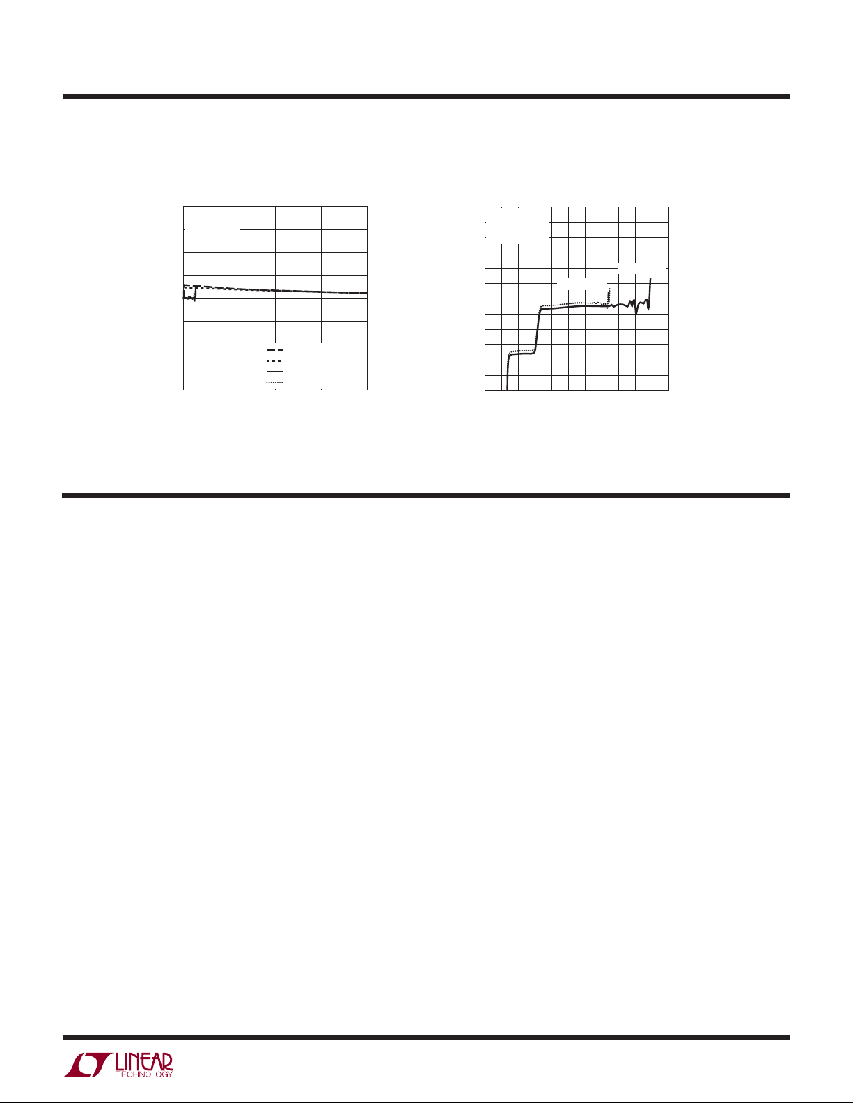
TYPICAL PERFORMANCE CHARACTERISTICS
Charging Current Error Charging Voltage Error
0.4
VDD = 5V
TEMP = 27°C
0.3
0.2
0.1
–0.1
–0.2
OUTPUT CURRENT ERROR (A)
–0.3
–0.4
= 12V
V
LOAD
0
0
1
CHARGING CURRENT (A)
DCIN = 15V, NoLowI
DCIN = 20V, NoLowI
DCIN = 15V, LowI
DCIN = 20V, LowI
2
43
4100 G10
0.150
0.125
0.100
0.075
0.050
0.025
0
–0.025
–0.050
–0.075
OUTPUT VOLTAGE ERROR (V)
–0.100
–0.125
–0.150
0
VDD = 5V
TEMP = 27°C
= 0.120A
I
LOAD
DCIN = 15V
42 6 10 14 18
8
CHARGING VOLTAGE (V)
LTC4100
DCIN = 20V
12
16
2220
4100 G11
PIN FUNCTIONS
TGATE (Pin 1): Drives the Top External P-MOSFET of the
Battery Charger Buck Converter.
PGND (Pin 2): High Current Ground Return for BGATE
Driver.
BGATE (Pin 3): Drives the Bottom External N-MOSFET of
the Battery Charger Buck Converter.
INFET (Pin 4): Drives the Gate of the External Input
P-MOSFET.
DCIN (Pin 5): External DC Power Source Input. Bypass to
ground with a 0.1µF capacitor.
CHGEN (Pin 6): Digital Bidirectional Pin to Enable Charger
Function. This pin is connected as a wired AND bus.
The following events will cause the POWER_FAIL bit in
the ChargerStatus register to become set:
1. An external device pulling the CHGEN signal to within
0.9V to GND;
2. The AC adapter voltage is not above the battery voltage.
SMBALERT (Pin 7): Active Low Interrupt Output to Host
(referred to as the SMBALERT# signal in the SMBus Revision 1.1 specifi cation). Signals host that there has been a
change of status in the charger registers and that the host
should read the LTC4100 status registers to determine if
any action on its part is required. This signal can be connected to the optional SMBALERT# line of the SMBus.
Open drain with weak current source pull-up to V
DD
(with
Schottky to allow it to be pulled to 5V externally).
SDA (Pin 8): SMBus Data Signal from Main (host-controlled) SMBus. External pull-up resistor is required.
SCL (Pin 9): SMBus Clock Signal from Main (host-controlled) SMBus. External pull-up resistor is required.
ACP (Pin 10): This Output Indicates the Value of the
DCDIV Comparator. It can be used to indicate whether
AC is present or not.
DCDIV (Pin 11): Supply Divider Input. This is a high impedance comparator input with a 1.2V threshold (rising
edge) and hysteresis.
GND (Pin 12): Ground for Digital and Analog Circuitry.
4100fb
7
Page 8

LTC4100
PIN FUNCTIONS
I
(Pin 13): An external resistor is connected between this
LIM
pin and GND. The value of the external resistor programs
the range and resolution of the programmed charger current. This is a digital, not an analog, function.
(Pin 14): An external resistor is connected between
V
LIM
this pin and GND. The value of the external resistor programs the range and resolution of the charging voltage.
This is a digital, not an analog, function.
THB (Pin 15): SafetySignal Force/Sense Pin to Smart
Battery. See description of operation for more detail. The
maximum allowed combined capacitance on THA, THB and
SafetySignal is 1nF (see Figure 4). A series resistor 54.9k
needs to be connected between this pin and the battery’s
SafetySignal for this circuit to work correctly.
THA (Pin 16): SafetySignal Force/Sense Pin to Smart
Battery. See description of operation for more detail. The
maximum allowed combined capacitance on THA, THB
and SafetySignal is 1nF (see Figure 4). A series resistor
1130 needs to be connected between this pin and the
battery’s SafetySignal for this circuit to work correctly.
(Pin 17): Power Supply Input for the LTC4100 Digital
V
DD
Circuitry. Bypass this pin with 0.1µF. Typically between
3.3V and 5V
DC
.
(Pin 19): Control Signal of the Inner Loop of the Current
I
TH
Mode PWM. Higher I
current in normal operation. A 0.0015µF capacitor to GND
fi lters out PWM ripple. Typical full-scale output current is
40µA. Nominal voltage range for this pin is 0V to 3V.
(Pin 20): Bypass to GND with a 0.068µF Capacitor.
I
DC
CSP (Pin 21): Current Amplifi er CA1 Input. This pin
and the BAT pin measure the voltage across the sense
resistor, R
signals required for both peak and average current mode
operation.
BAT (Pin 22): Battery Sense Input and the Negative Reference for the Current Sense Resistor. A bypass capacitor
of at least 10µF is required.
CLN (Pin 23): Negative Input to the Input Current Limiting
Circuit Block. If no current limit function is desired, connect
this pin to CLP. The threshold is set at 100mV below the
voltage at the CLP pin. When used to limit supply current,
a fi lter is needed to fi lter out the switching noise.
CLP (Pin 24): Positive Input to the Input Current Limiting
Circuit Block. This pin also serves as a power supply for
the IC.
, to provide the instantaneous current
SENSE
corresponds to higher charging
TH
(Pin 18): Tap Point of the Programmable Resistor
V
SET
Divider, which Provides Battery Voltage Feedback to the
Charger.
4100fb
8
Page 9

BLOCK DIAGRAM
LTC4100
V
BAT
SYSTEM
LOAD
CSP
R1
R
CL
Q1
V
IN
TO HOST AND BATTERY
1.13k
54.9k
100
L1
D1
10k
R4
C5, 0.1µF
Q2
Q3
C9
C1, 0.1µF
C4
0.01µF
20µF
SMBALERT
V
SET
GND
TGATE
BGATE
PGND
CLN
CLP
DCIN
INFET
CHGEN
SDA
SCL
THA
THB
V
20µF
R
ILIM
BAT
C7
0.0015µF
V
IN
–
+
+
–
–
+
10-BIT
I
DAC
3k
11.67µA
3k
9k
17mV
1.19V
1.2V
CA1
BUFFERED
÷5
I
CMP
I
REV
gm = 1m
–
+
–
+
I
TH
CA2
LIMIT
DECODER
18
11-BIT
V
10µA
t
PWM
LOGIC
DAC
1.28V
ON
1.19V
100mV
V
DD
SMBus
INTERFACE
AND CONTROL
THERMISTER
INTERFACE
–
+
+
–
EA
Q
CL1
0V
gm = 1m
S
R
gm = 1.5m
CLP
12
1
3
2
23
24
5
4
6
7
8
9
16
15
CLP
DCIN
OSCILLATOR
WATCHDOG
DETECT
5.8V
22
R
21
20
19
10
11
17
13
14
BAT
SENSE
CSP
CSP
I
DC
I
TH
C6, 0.12µF
ACP
DCDIV
R11
V
TO SMBUS
DD
POWER SUPPLY
I
LIM
V
LIM
R
VLIM
C8
0.068µF
R5, 6.04k
R10
Figure 2
4100fb
9
Page 10
LTC4100
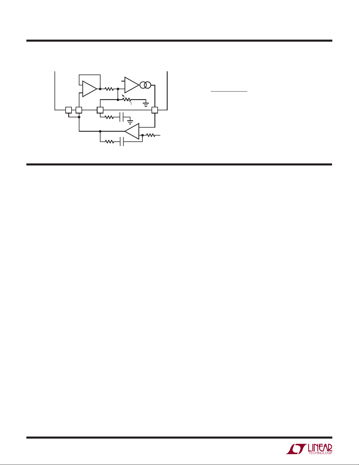
TEST CIRCUIT
+
SET
1.19V
LT1055
EA
–
V
DAC
–
+
21 22 18 19
CSP
BAT
V
LTC4100
I
TH
+
–
0.6V
4100 TC01
OPERATION
Overview (Refer to Block Diagram)
The LTC4100 is composed of a battery charger section, a
charger controller, a 10-bit DAC to control charger current,
an 11-bit DAC to control charger voltage, a SafetySignal
decoder, limit decoder and an SMBus controller block. If
no battery is present, the SafetySignal decoder indicates
a RES_OR condition and charging is disabled by the
charger controller (CHGEN = Low). Charging will also be
disabled if DCDIV is low, or the SafetySignal is decoded
as RES_HOT. If a battery is inserted and AC power is
connected, the battery will be charged with an 80mA
“wake-up” current. The wake-up current is discontinued
after t
TIMEOUT
or RES_C0LD, and the battery or host doesn’t transmit
charging commands.
if the SafetySignal is decoded as RES_UR
VV
–
V
TOL
BAT VDAC
=
V
VDAC
FOR V V x A
VDAC
DCIN V
=
21
CLN CLP V
==
•
100
=
.( )
17 57 0 44 0
20
charger controller asserts the CHGEN line if the decoded
SafetySignal value will allow charging to commence. ChargingCurrent() and ChargingVoltage() values are compared
against limits programmed by the limit decoder block; if
the commands exceed the programmed limits these limits
are substituted and overrange fl ags are set.
The charger controller will assert SMBALERT whenever a status change is detected, namely: AC_PRESENT,
BATTERY_PRESENT, ALARM_INHIBITED, or V
power-
DD
fail. The host may query the charger, via the SMBus, to
obtain ChargerStatus() information. SMBALERT will be
deasserted upon a successful read of ChargerStatus() or
a successful Alert Response Address (ARA) request.
Battery Charger Controller
The SMBus interface and control block receives ChargingCurrent() and ChargingVoltage() commands via the
SMBus. If ChargingCurrent() and ChargingVoltage()
command pairs are received within a t
TIMEOUT
interval, the
values are stored in the current and voltage DACs and the
10
The LTC4100 charger controller uses a constant off-time,
current mode step-down architecture. During normal
operation, the top MOSFET is turned on each cycle when
the oscillator sets the SR latch and turned off when
the main current comparator I
resets the SR latch.
CMP
4100fb
Page 11

OPERATION
LTC4100
While the top MOSFET is off, the bottom MOSFET is
turned on until either the inductor current trips the current
comparator I
, or the beginning of the next cycle. The
REV
oscillator uses the equation,
VV
(–)
t
OFF
DCIN BAT
=
Vf
(•)
DCIN OSC
to set the bottom MOSFET on-time. The result is quasiconstant frequency operation: the converter frequency
remains nearly constant over a wide range of output
voltages. This activity is diagrammed in Figure 3.
The peak inductor current, at which I
latch, is controlled by the voltage on I
resets the SR
CMP
. ITH is in turn
TH
controlled by several loops, depending upon the situation
at hand. The average current control loop converts the
voltage between CSP and BAT to a representative current.
Error amp CA2 compares this current against the desired
current programmed by the I
for the desired voltage across R
I
TH
DAC
at the I
pin and adjusts
DC
.
SENSE
The voltage at BAT is divided down by an internal resistor divider set by the V
to decrease I
if the divider voltage is above the 1.19V
TH
and is used by error amp EA
DAC
reference.
The amplifi er CL1 monitors and limits the input current,
normally from the AC adapter, to a preset level (100mV/R
At input current limit, CL1 will decrease the I
voltage to
TH
CL
).
reduce charging current.
An overvoltage comparator, OV, guards against transient
overshoots (>7%). In this case, the top MOSFET is turned
off until the overvoltage condition is cleared. This feature
is useful for batteries that “load dump” themselves by
opening their protection switch to perform functions such
as calibration or pulse mode charging.
OFF
TGATE
ON
ON
BGATE
OFF
INDUCTOR
CURRENT
t
OFF
TRIP POINT SET
VOLTAGE
BY I
TH
4100 F03
PWM Watchdog Timer
There is a watchdog timer that observes the activity on
the TGATE pin. If TGATE stops switching for more than
40µs, the watchdog activates and turns off the top MOSFET
for about 400ns. The watchdog engages to prevent very
low frequency operation in dropout—a potential source
of audible noise when using ceramic input and output
capacitors.
Charger Start-Up
When the charger is enabled, it will not begin switching
until the I
voltage exceeds a threshold that assures initial
TH
current will be positive. This threshold is 5% to 15% of the
maximum programmed current. After the charger begins
switching, the various loops will control the current at a
level that is higher or lower than the initial current. The
duration of this transient condition depends upon the loop
compensation, but is typically less than 1ms.
SMBus Interface
All communications over the SMBus are interpreted by the
SMBus interface block. The SMBus interface is a SMBus
slave device at address 0x12. All internal LTC4100 registers
may be updated and accessed through the SMBus interface,
and charger controller as required. The SMBus protocol
is a derivative of the I
to Use It, V1.0
Specifi cation
by Philips, and
, Version 1.1, from the SBS Implementers
C bus (Reference
System Management Bus
I2C-Bus and How
2
Forum, for a complete description of the bus protocol
requirements.)
All data is clocked into the shift register on the rising edge
of SCL. All data is clocked out of the shift register on the
falling edge of SCL. Detection of an SMBus Stop condition, or power-on reset via the V
power-fail, will reset
DD
the SMBus interface to an initial state at any time.
The LTC4100 command set is interpreted by the SMBus
interface and passed onto the charger controller block as
control signals or updates to internal registers.
Figure 3
*http://www. SBS-FORUM.org
4100fb
11
Page 12

LTC4100
OPERATION
Description of Supported Battery Charger Functions
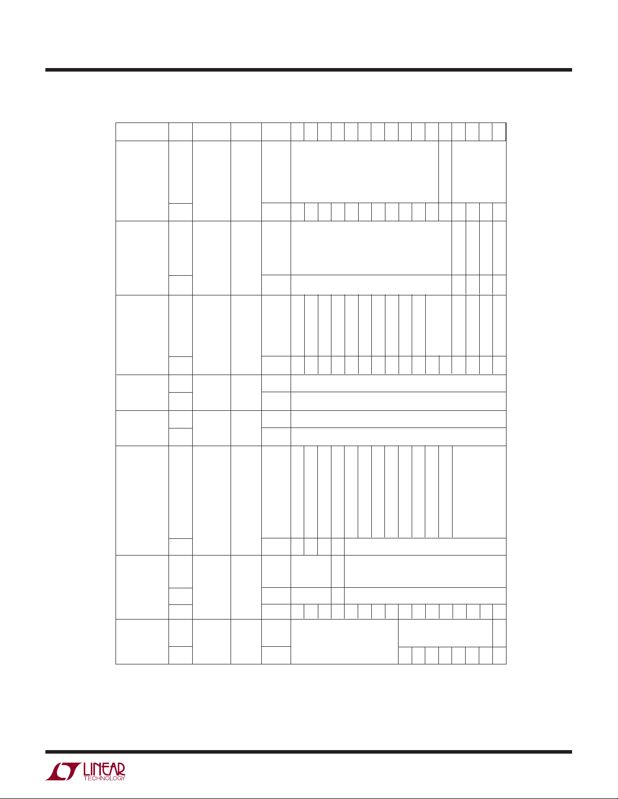
The functions are described as follows (see Table 1 also):
FunctionName() ‘hnn (command code)
Description: A brief description of the function.
Purpose: The purpose of the function, and an example
where appropriate.
• SMBus Protocol: Refer to Section 5 of the Smart
Battery Charger specifi cation for more details.
Input, Output or Input/Output: A description of the data
supplied to or returned by the function.
ChargerSpecInfo() (‘h11)
Description: The SMBus Host uses this command to read
the LTC4100’s extended status bits.
Purpose: Allows the System Host to determine the
specifi cation revision the charger supports as well as
other extended status information.
• SMBus Protocol: Read Word.
Output: The CHARGER_SPEC indicates that the LTC4100
supports Version 1.1 of the Smart Battery Charger
Specifi cation. The SELECTOR_SUPPORT indicates that
the LTC4100 does not support the optional Smart Battery
Selector Commands.
ChargerMode() (‘h12)
Description: The SMBus Host uses this command to set
the various charger modes. The default values are set to
allow a Smart Battery and the LTC4100 to work in concert
without requiring an SMBus Host.
Purpose: Allows the SMBus Host to confi gure the charger
and change the default modes. This is a write only function,
but the value of the “mode” bit, INHIBIT_CHARGE may be
determined using the ChargerStatus() function.
• SMBus Protocol: Write Word.
Input: The INHIBIT_CHARGE bit allows charging to be
inhibited without changing the ChargingCurrent() and
ChargingVoltage() values. The charging may be resumed
by clearing this bit. This bit is automatically cleared when
power is reapplied or when a battery is reinserted.
The ENABLE_POLLING bit is not supported by the LTC4100.
Values written to this bit are ignored.
The POR_RESET bit sets the LTC4100 to its power-on
default condition.
The RESET_TO_ZERO bit sets the ChargingCurrent()and
ChargingVoltage() values to zero. This function ALWAYS
clears the ChargingVoltage() and ChargingCurrent() values
to zero even if the INHIBIT_CHARGE bit is set.
ChargerStatus() (‘h13)
Description: The SMBus Host uses this command to read
the LTC4100’s status bits.
Purpose: Allows the SMBus Host to determine the status
and level of the LTC4100.
• SMBus Protocol: Read Word.
Output: The CHARGE_INHIBITED bit refl ects the status
of the LTC4100 set by the INHIBIT_CHARGE bit in the
ChargerMode() function.
The POLLING_ENABLED, VOLTAGE_NOTREG, and CURRENT_NOTREG are not supported by the LTC4100.
The LTC4100 always reports itself as a Level 2 Smart
Battery Charger.
CURRENT_OR bit is set only when ChargingCurrent() is
set to a value outside the current regulation range of the
LTC4100. This bit may be used in conjunction with the
INHIBIT_CHARGE bit of the ChargerMode() and ChargingCurrent() to determine the current capability of the
LTC4100. When ChargingCurrent() is set to the I
the CURRENT_OR bit will be set.
VOLTAGE_OR bit is set only when ChargingVoltage() is
set to a value outside the voltage regulation range of the
LTC4100. This bit may be used in conjunction with the
INHIBIT_CHARGE bit of the ChargerMode() and ChargingVoltage() to determine the voltage capability of the
LTC4100. When ChargingVoltage() is set to the V
VOLTAGE_OR bit will be set.
The RES_OR bit is set only when the SafetySignal resistance value is greater than 95k. This indicates that the
SafetySignal is to be considered as an open circuit.
LIM
LIM
+ 1,
, the
12
4100fb
Page 13
OPERATION
Table 1. Summary of Supported Charger Functions
Function
ChargerSpecInfo() 7'b0001_001 8'h11 Info
ChargerMode() 7'b0001_001 8'h12 Control
ChargerStatus() 7'b0001_001 8'h13 Status
ChargingCurrent() 7'b0001_001 8'h14 Value CHARGING_CURRENT[15:0]
ChargingVoltage() 7'b0001_001 8'h15 Value CHARGING_VOLTAGE[15:0]
AlarmWarning() 7'b0001_001 8'h16 Control
SMBus
Access
Address
(0x12)
Return
Read Values
Permitted
Write Values
Return
Read Values
Permitted
Write Values
Permitted
Write Values
Command
Code
Data
Typ e
D15 D14 D13 D12 D11 D10 D9 D8 D7 D6 D5 D4 D3 D2 D1 DO
0 0 0 0 0 0 0 0 0 0 0 0 0 0 1 0
1/0 1/0 Ign 1/0
AC_PRESENT
BATTERY_PRESENT
1/0 1/0 1/0 1/0 1/0 1/0 1/0 1/0 1/0 1/0 0 1 0 0 0 1/0
Reserved
Reserved
Ignored
POWER_FAIL
ALARM_INHIBITED
RES_UR
RES_HOT
RES_COLD
RES_OR
VOLTAGE_OR
Unsigned integer representing current in mA
Unsigned integer representing voltage in mV
SELECTOR_SUPPORT
CURRENT_OR
LEVEL:3/LEVEL:2
LTC4100
CHARGER_SPEC
RESET_TO_ZERO
POR_RESET
ENABLE_POLLING
CURRENT_NOTREG
VOLTAGE_NOTREG
POLLING_ENABLED
INHIBIT_CHARGE
CHARGE_INHIBITED
OVER_CHARGED_ALARM
TERMINATE_CHARGE_ALARM
RESERVED_ALARM
OVER_TEMP_ALARM
TERMINATE_DISCHARGE_ALARM
Reserved
REMAINING_CAPACITY_ALARM
REMAINING_TIME_ALARM
INITIALIZED
DISCHARGING
FULLY_CHARGED
Permitted
Write Values
LTCO() 7'b0001_001 8'h3C Register
Alert Response 7'b0001_100 N/A Status LTC4100's Address
Address (0x18)
Permitted
Write Values
Return
Read Values
Read
Byte
1/0 1/0 1/0 1/0
Reserved
Ignored
0 0 0 1/0 0 0 1 0 0 0 0 0 0 0 1 0
Return
0 0 0 1 0 0 1 X
Values
NO_LOWI
1/0
Not Supported
Ignored
LTC4100's Version Identification
Ignored
FULLY DISCHARGED
ERROR
Undefined
4100fb
13
Page 14
LTC4100
OPERATION
The RES_COLD bit is set only when the SafetySignal resistance value is greater than 28.5k. The SafetySignal
indicates a cold battery. The RES_COLD bit will be set
whenever the RES_OR bit is set.
The RES_HOT bit is set only when the SafetySignal resistance is less than 3150, which indicates a hot battery.
The RES_HOT bit will be set whenever the RES_UR bit
is set.
The RES_UR bit is set only when the SafetySignal resistance value is less than 575.
ALARM_INHIBITED bit is set if a valid AlarmWarning()
message has been received and charging is inhibited as
a result. This bit is cleared if both ChargingVoltage() and
ChargingCurrent() are rewritten to the LTC4100, power is
removed (DCDIV < V
), or if a battery is removed. The
ACP
setting of the ALARM_INHIBITED will activate the LTC4100
SMBALERT pull-down.
POWER_FAIL bit is set if the LTC4100 does not have suffi cient DCIN voltage to charge the battery or if an external
device is pulling the CHGEN input signal low. Charging is
disabled whenever this bit is set. The setting of this bit
does not clear the values in the ChargingVoltage() and
ChargingCurrent() function values, nor does it necessarily
affect the charging modes of the LTC4100.
BATTERY_PRESENT is set if a battery is present otherwise it is cleared. The LTC4100 uses the SafetySignal
in order to determine battery presence. If the LTC4100
detects a RES_OR condition, the BATTERY_PRESENT
bit is cleared immediately. The LTC4100 will not set the
BATTERY_PRESENT bit until it successfully samples the
SafetySignal twice and does not detect a RES_OR condition on either sampling. If AC is not present (e.g. DCDIV
), this bit may not be set for up to one-half second
< V
ACP
after the battery is connected to the SafetySignal. The
ChargingCurrent() and ChargingVoltage() function values are immediately cleared whenever this bit is cleared.
Charging will never be allowed if this bit is cleared. A
change in BATTERY_PRESENT will activate the LTC4100
SMBALERT pull-down.
AC_PRESENT is set if the voltage on DCDIV is greater than
. This does not necessarily indicate that the voltage
V
ACP
on DCIN is suffi cient to charge the battery. A change in
AC_PRESENT will activate the LTC4100 SMBALERT pulldown.
ChargingCurrent() (‘h14)
Description: The Battery, System Host or other master
device sends the desired charging current (mA) to the
LTC4100 .
Purpose: The LTC4100 uses R
, and the value of the ChargingCurrent() function to
I
DAC
, the granularity of the
ILIM
determine its charging current supplied to the battery. The
charging current will never exceed the maximum current
permitted by R
truncated to the granularity of the I
. The ChargingCurrent() value will be
ILIM
. The charging cur-
DAC
rent will also be reduced if the battery voltage exceeds the
programmed charging voltage.
• SMBus Protocol: Write Word.
Input: The CHARGING_CURRENT is an unsigned 16 bit
integer specifying the requested charging current in mA.
The following table defi nes the maximum permissible
value of CHARGING_CURRENT that will not set the CURRENT_OR in the ChargerStatus() function for a given
value of the R
R
ILIM
Short to GND 0x0000 through 0x03FF 0mA through 1023mA
10k ±1% 0x0000 through 0x07FF 0mA through 2047mA
33k ±1% 0x0000 through 0x0BFF 0mA through 3071mA
Open (or Short to V
:
ILIM
ChargingCurrent() Current
) 0x0000 through 0x0FFF 0mA through 4095mA
DD
ChargingVoltage() (‘h15)
Description: The Battery, SMBus Host or other master
device sends the desired charging voltage (mV) to the
LTC4100.
Purpose: The LTC4100 uses R
, and the value of the ChargingVoltage() function to
V
DAC
, the granularity of the
VLIM
determine its charging voltage supplied to the battery. The
charging voltage will never be forced beyond the voltage
permitted by R
truncated to the granularity of the V
. The ChargingVoltage() value will be
VLIM
. The charging
DAC
voltage will also be reduced if the battery current exceeds
the programmed charging current.
• SMBus Protocol: Write Word.
4100fb
14
Page 15

OPERATION
LTC4100
Input: The CHARGING_VOLTAGE is an unsigned 16-bit
integer specifying the requested charging voltage in mV.
The LTC4100 considers any value from 0x0001 through
0x049F the same as writing 0x0000. The following
table defi nes the maximum permissible value of CHARGING_VOLTAGE that will not set the VOLTAGE_OR in the
ChargerStatus() function for a given value of R
R
VLIM
Short to GND 0x225F (8796mV)
10k ±1% 0x332F (13100mV)
33k ±1% 0x43FF (17404mV)
100k ±1% 0x54CF (21708mV)
Open (or Short to V
) 0x6D5F (27996mV)
DD
Maximum ChargingVoltage()
VLIM
:
AlarmWarning() (‘h16)
Description: The Smart Battery, acting as a bus master
device, sends the AlarmWarning() message to the LTC4100
to notify it that one or more alarm conditions exist. Alarm
indications are encoded as bit fi elds in the Battery’s Status register, which is then sent to the LTC4100 by this
function.
Purpose: The LTC4100 will use the information sent by
this function to properly charge the battery. The LTC4100
will only respond to certain alarm bits. Writing to this
function does not necessarily cause an alarm condition
that inhibits battery charging.
• SMBus Protocol: Write Word.
Input: Only the OVER_CHARGED_ALARM, TERMINATE
_CHARGE_ALARM, reserved (0x2000), and OVER
_TEMP_ALARM bits are supported by the LTC4100.
Writing a one to any of these specifi ed bits will inhibit
the charging by the LTC4100 and will set the ALARM_
INHIBITED bit in the ChargerStatus() function. The
TERMINATE_DISCHARGE_ALARM, REMAINING_
CAPACITY_ALARM, REMAINING_TIME_ALARM, and the
ERROR bits are ignored by the LTC4100.
LTC0() (‘h3C)
Purpose: This function allows the SMBus Host to deter-
mine if the battery charger is an LTC4100. Identifying the
manufacturer and version of the Smart Battery Charger
permits software to perform tasks specifi c to a given
charger. The LTC4100 also provides a means of disabling
the LOWI current mode of the I
DAC
.
• SMBus Protocol: Write Word.
Input: The NO_LOWI is the only bit recognized by this
function. The default value of NO_LOWI is zero. The
LTC4100 LOWI current mode provides a more accurate
average charge current when the charge current is less
than 1/16 of the full scale I
is set, a less accurate I
value. When the NO_LOWI
DAC
algorithm is used to generate
DAC
the charging current, but because the charger is not pulsed
on and off, it may be preferred.
• SMBus Protocol: Read Word.
Output: The NO_LOWI indicates the I
mode of opera-
DAC
tion. If clear, then the LOWI current mode will be used
when the charging current is less than 1/16 of the full-
DAC
value.
scale I
The LTC Version Identifi cation will always be 0x202 for
the LTC4100.
Alert Response Address (ARA)
Description: The SMBus system host uses the Alert
Response Address to quickly identify the generator of an
SMBALERT# event.
Purpose: The LTC4100 will respond to an ARA address
0x18 if the SMBALERT signal is actively pulling down the
SMBALERT# bus. The LTC4100 will follow the prioritization reporting as defi ned in the System Management Bus
Specifi cation, Version 1.1, from the SBS Implementers
Forum.
• SMBus Protocol: A 7-bit Addressable Device Responds
to an ARA.
Output: The Device Address will be sent to the SMBus
system host. The LTC4100 Device address is 0x12.
Description: The SMBus Host uses this command to
determine the version number of the LTC4100 and set
extended operation modes not defi ned by the Smart Battery Charger Specifi cation.
The following events will cause the LTC4100 to pull-down
the SMBALERT# bus through the SMBALERT pin:
• Change of AC_PRESENT in the ChargerStatus() function.
4100fb
15
Page 16

LTC4100
OPERATION
• Change of BATTERY_PRESENT in the ChargerStatus()
function.
• Setting ALARM_INHIBITED in the ChargerStatus()
function.
• Internal power-on reset condition.
SMBus Accelerator Pull-Ups
Both SCL and SDA have SMBus accelerator circuits
which reduce the rise time on systems with signifi cant
capacitance on the two SMBus signals. The dynamic pull-up
circuitry detects a rising edge on SDA or SCL and applies
1mA to 10mA pull-up to V
– 0.8V (external pull-up resistors are still required
< V
DD
to supply DC current). This action allows the bus to meet
SMBus rise time requirements with as much as 250pF on
each SMBus signal. The improved rise time will benefi t
all of the devices which use the SMBus, especially those
devices that use the I
pull-up circuits only pull to V
that are not compliant to the SMBus specifi cations may still
have rise time compliance problems if the SMBus pull-up
resistors are terminated with voltages higher than V
The Control Block
2
C logic levels. Note that the dynamic
when VIN > 0.8V until VIN
DD
, so some SMBus devices
DD
DD
.
3. The host may control charging by disabling the Smart
Battery’s ability to transmit ChargingCurrent() and
ChargingVoltage() request functions and broadcasting the charging commands to the LTC4100 over the
SMBus.
4. The LTC4100 will still respond to Smart Battery critical
warning messages without host intervention.
Wake-Up Charging Mode
The following conditions must be met in order to allow
wake-up charging of the battery:
1. The SafetySignal must be RES_COLD, RES_IDEAL, or
RES_UR.
2. AC must be present. This is qualifi ed by DCDIV >
.
V
ACP
Wake-up charging initiates when a newly inserted battery
does not send ChargingCurrent() and ChargingVoltage()
functions to the LTC4100.
The following conditions will terminate the wake-up
charging mode.
1. A T
TIMEOUT
RES_COLD or RES_UR.
period is reached when the SafetySignal is
The LTC4100 charger operations are handled by the control block. This block is capable of charging the selected
battery autonomously or under SMBus Host control.
The control block can request communications with the
system management host (SMBus Host) by asserting
SMBALERT = 0; this will cause the SMBus Host, if present,
to poll the LTC4100.
The control block receives SMBus slave commands from
the SMBus interface block.
The control block allows the LTC4100 to meet the following Smart Battery-controlled (Level 2) charger requirements:
1. Implements the Smart Battery’s critical warning messages over the SMBus.
2. Operates as an SMBus slave device that responds to
ChargingVoltage() and ChargingCurrent() commands and
adjusts the charger output parameters accordingly.
2. The SafetySignal is registering RES_OR.
3. The successful writing of the ChargingCurrent() AND
ChargingVoltage() function. The LTC4100 will proceed
to the controlled charging mode after these two functions are written.
4. The SafetySignal is registering RES_HOT.
5. The AC power is no longer present. (DCDIV < V
6. The ALARM_INHIBITED becomes set in the ChargerStatus() function.
7. The INHIBIT_CHARGE is set in the ChargerMode()
function.
8. The CHGEN pin is pulled low by an external device. The
LTC4100 will resume wake-up charging, if the CHGEN
pin is released by the external device. Toggling the
CHGEN pin will not reset the T
TIMEOUT
timer.
ACP
)
4100fb
16
Page 17
OPERATION
LTC4100
9. There is insuffi cient DCIN voltage to charge the battery.
The LTC4100 will resume wake-up charging when there
is suffi cient DCIN voltage to charge the battery. This
condition will not reset the T
TIMEOUT
timer.
Controlled Charging Algorithm Overview
The following conditions must be met in order to allow
controlled charging to start on the LTC4100:
1. The ChargingVoltage() AND ChargingCurrent() function
must be written to non-zero values.
2. The SafetySignal must be RES_COLD, RES_IDEAL, or
RES_UR.
3. AC must be present. This is qualifi ed by DCDIV >
.
V
ACP
The following conditions will stop the controlled charging
algorithm and will cause the battery charger controller to
stop charging:
1. The ChargingCurrent() AND ChargingVoltage() functions
have not been written for T
TIMEOUT
.
2. The SafetySignal is registering RES_OR.
3. The SafetySignal is registering RES_HOT.
4. The AC power is no longer present. (DCDIV < V
ACP
)
5. ALARM_INHIBITED is set in the ChargerStatus()
function.
6. INHIBIT_CHARGE is set in the ChargerMode() function.
Clearing INHIBIT_CHARGE will cause the LTC4100 to
resume charging using the previous ChargingVoltage()
AND ChargingCurrent() function values.
7. RESET_TO_ZERO is set in the ChargerMode() function.
8. CHGEN pin is pulled low by an external device. The
LTC4100 will resume charging using the previous
ChargingVoltage() AND ChargingCurrent() function
values, if the CHGEN pin is released by the external
device.
9. Insuffi cient DCIN voltage to charge the battery. The
LTC4100 will resume charging using the previous
ChargingVoltage() AND ChargingCurrent() function
values, when there is suffi cient DCIN voltage to charge
the battery.
10. Writing a zero value to ChargingVoltage() function.
11. Writing a zero value to ChargingCurrent() function.
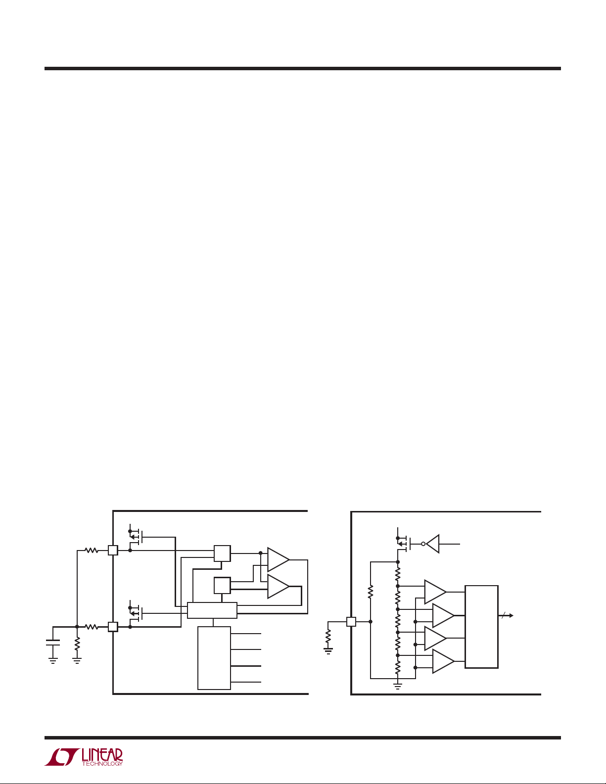
The SafetySignal Decoder Block
This block measures the resistance of the SafetySignal and
features high noise immunity at critical trip points. The low
power standby mode supports only battery presence SMB
charger reporting requirements when AC is not present.
The SafetySignal decoder is shown in Figure 4. The value
of R
is 1.13k and R
THA
is 54.9k.
THB
V
DD
V
DD
THA_SELB
THB_SELB
MUX
REF
SafetySignal
CONTROL
LATCH
HI_REF
LO_REF
RES_OR
RES_COLD
RES_H0T
RES_UR
+
TH_HI
–
+
TH_LO
–
4100 F04
33k
V
LIM
14
R
VLIM
Figure 5. Simplifi ed V
R
THA
1.13k
16
THA
R
THB
54.9k
15
R
SafetySignal
THB
C
SS
Figure 4. SafetySignal Decoder Block
12.5k
25k
25k
25k
12.5k
V
DD
+
–
+
–
Circuit Concept (I
LIM
AC_PRESENT
+
–
+
–
ENCODER
4
is Similar)
LIM
V
[3:0]
LIM
4100 F05
4100fb
17
Page 18

LTC4100
OPERATION
SafetySignal sensing is accomplished by a state machine
that reconfi gures the switches of Figure 4 using THA_SELB
and THB_SELB, a selectable reference generator, and two
comparators. This circuit has two modes of operation
based upon whether AC is present.
When AC is present, the LTC4100 samples the value of
the SafetySignal and updates the ChargerStatus register
approximately every 32ms. The state machine successively
samples the SafetySignal value starting with the RES_OR
≥ RES_COLD threshold, then RES_C0LD ≥ RES_IDEAL
threshold, RES_IDEAL ≥ RES_HOT threshold, and fi nally
the RES_HOT ≥ RES_UR threshold. Once the SafetySignal range is determined, the lower value thresholds are
not sampled. The SafetySignal decoder block uses the
previously determined SafetySignal value to provide the
appropriate adjustment in threshold to add hysteresis.
The R
resistor value is used to measure the RES_OR
THB
≥ RES_COLD and RES_COLD ≥ RES_IDEAL thresholds by
connecting the THB pin to V
resultant on the THA pin. The R
and measuring the voltage
DD
resistor value is used
THA
to measure the RES_IDEAL ≥ RES_HOT and RES_HOT ≥
RES_UR thresholds by connecting the THA pin to V
DD
and
measuring the voltage resultant on the THB pin.
The SafetySignal decoder block uses a voltage divider
network between V
and GND to determine SafetySig-
DD
nal range thresholds. Since the THA and THB inputs are
sequentially connected to V
, this provides VDD noise
DD
immunity during SafetySignal measurement.
When AC power is not available the SafetySignal block
supports the following low power operating features:
1. The SafetySignal is sampled every 250ms or less,
instead of 32ms.
The SafetySignal impedance is interpreted according to
Table 4.
Table 4. SafetySignal State Ranges
SafetySignal
RESISTANCE
0 to 500 RES_UR
500 to 3k RES_HOT
3k to 30k BATTERY_PRESENT Ideal
30k to 100k RES_COLD
Above 100k RES_OR RES_COLD Overrange
Note: The underrange detection scheme is a very important feature of the
LTC4100. The R
well above the 0.047 • V
pull-up. A system using a 10k pull-up would not be able to resolve the
important underrange to hot transition point with a modest 100mV of
ground offset between battery and SafetySignal detection circuitry. Such
offsets are anticipated when charging at normal current levels.
The required values for R
CHARGE STATUS BITS DESCRIPTION
RES_HOT
BATTERY_PRESENT
BATTERY_PRESENT
BATTERY_PRESENT
THA/RSafetySignal
divider trip point of 0.333 • VDD (1V) is
(140mV) threshold of a system using a 10k
DD
and R
THA
THB
Underrange
Hot
Cold
are shown in
Table 5.
Table 5. SafetySignal External Resistor Values
EXTERNAL RESISTOR VALUE (Ω)
R
THA
R
THB
1130 ±1%
54.9k ±1%
CSS represents the capacitance between the SafetySignal
and GND. C
immunity from transients in the application. C
may be added to provide additional noise
SS
cannot
SS
exceed 1nF if the LTC4100 is to properly sense the value
of R
SafetySignal
.
2. A full SafetySignal status is sampled every 30s or less,
instead of every 32ms.
18
4100fb
Page 19
OPERATION
LTC4100
The I
Decoder Block
LIM
The value of an external resistor connected from this pin
to GND determines one of four current limits that are used
for maximum charging current value. These limits provide
a measure of safety with a hardware restriction on charging
current which cannot be overridden by software.
Table 6. I
EXTERNAL
RESISTOR
(R
ILIM
Short to GND V
10k ±1% 0.17V
33k ±1% 0.42V
Open (>250k,
or Short to VDD)
The V
Trip Points and Ranges
LIM
)I
Decoder Block
LIM
V
ILIM
ILIM
V
VOLTAGE
LIM
< 0.09V
< 0.34V
ILIM
0.66V
V
<
VDD
<
VDD
< 0.59V
<
VDD
ILIM
VDD
CONTROLLED
CHARGING
CURRENT RANGE GRANULARITY
0 < I < 1023mA 1mA
DD
0 < I < 2046mA 2mA
0 < I < 3068mA 4mA
0 < I < 4092mA 4mA
The value of an external resistor connected from this pin
to GND determines one of fi ve voltage limits that are applied to the charger output value. These limits provide a
measure of safety with a hardware restriction on charging
voltage which cannot be overridden by software.
Table 7. V
EXTERNAL
RESISTOR
(R
VLIM
Short to
GND
10k ±1% 0.17V
33k ±1% 0.42V
100k ±1% 0.66V
Open or
Tied to V
Trip Points and Ranges (See Figure 5)
LIM
CONTROLLED
)V
DD
V
VLIM
0.91V
VOLTAGE
LIM
< 0.09V
VDD
< 0.34V
VCCP
< 0.59V
VDD
< 0.84V
VDD
< V
VDD
< V
VDD
< V
VDD
< V
CHARGING VOLTAGE
(V
OUT
VCCP
VLIM
VLIM
VLIM
VLIM
2900mV < V
< 8800mV
2900mV < V
< 13104mV
2900mV < V
< 17408mV
2900mV < V
< 21712mV
2900mV < V
< 28000mV
) RANGE GRANULARITY
OUT
OUT
OUT
OUT
OUT
16mV
16mV
16mV
16mV
16mV
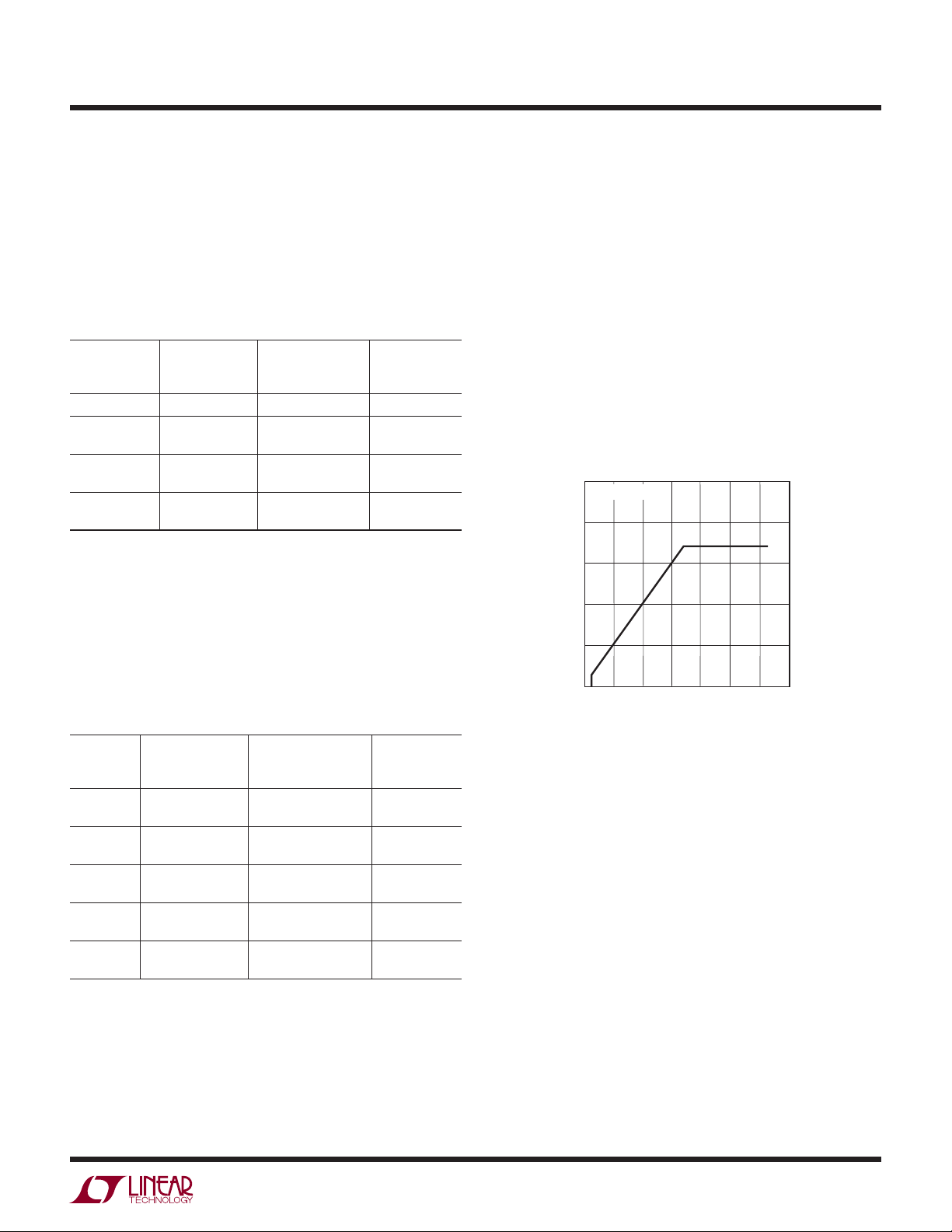
The Voltage DAC Block
Note that the charger output voltage is offset by V
Therefore, the value of V
is subtracted from the SMBus
REF
REF
.
ChargingVoltage() value in order for the output voltage to
be programmed properly (without offset). If the ChargingVoltage() value is below the nominal reference voltage of
the charger, nominally 1.184V, the charger output voltage
is programmed to zero. In addition, if the ChargingVoltage() value is above the limit set by the V
pin, then the
LIM
charger output voltage is set to the value determined by
the V
resistor and the VOLTAGE_OR bit is set. These
LIM
limits are demonstrated in Figure 6.
25
R
= 33k
VLIM
20
(V)
15
OUT
10
CHARGER V
5
0
0
NOTE: THE LTC4100 CAN BE PROGRAMMED WITH ChargingVoltage() FUNCTION VALUES
BETWEEN 1.184V AND 2.9V, HOWEVER, THE BATTERY CHARGER CONTROLLER OUTPUT
VOLTAGE MAY BE ZERO WITH PROGRAMMED VALUES BELOW 2.9V.
10
5
PROGRAMMED VALUE (V)
20
15
25
Figure 6. Transfer Function of Charger
35
30
4100 F06
4100fb
19
Page 20
LTC4100
OPERATION
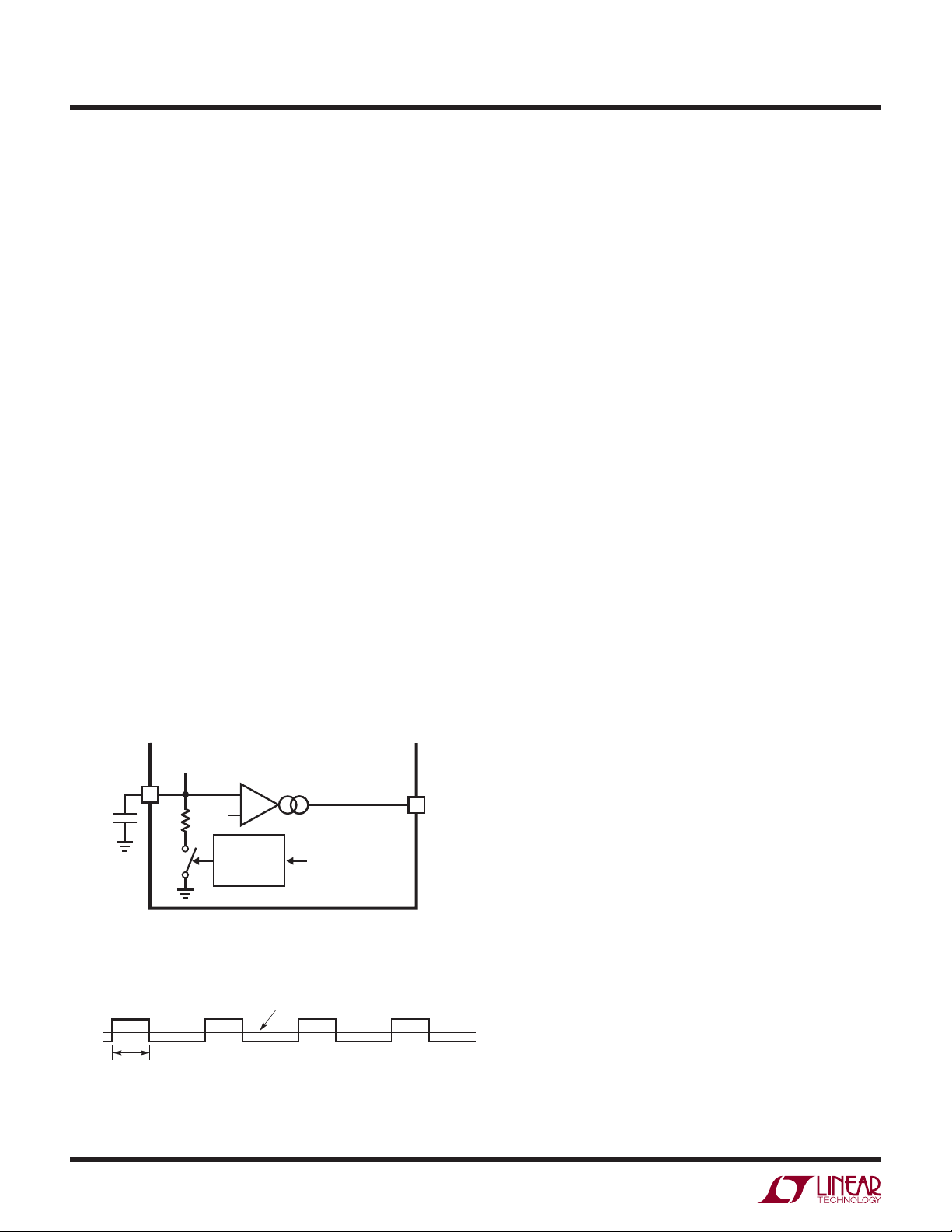
The Current DAC Block
The current DAC is a delta-sigma modulator which controls
the effective value of an external resistor, R
, used to
SET
set the current limit of the charger. Figure 7 is a simplifi ed
diagram of the DAC operation. The delta-sigma modulator
and switch convert the ChargingCurrent() value, received
via the SMBus, to a variable resistance equal to:
1.25R
/[ChargingCurrent()/I
SET
LIM[x]
] = R
IDC
Therefore, programmed current is equal to:
I
CHARGE
= (102.3mV/R
for ChargingCurrent() < I
) (ChargingCurrent()/I
SENSE
.
LIM[x]
LIM[x]
),
When a value less than 1/16th of the maximum current
allowed by I
is applied to the current DAC input, the
LIM
current DAC enters a different mode of operation called
LOWI. The current DAC output is pulse width modulated
with a high frequency clock having a duty cycle value of
1/8. Therefore, the maximum output current provided by
the charger is I
/8. The delta-sigma output gates this
MAX
low duty cycle signal on and off. The delta-sigma shift
registers are then clocked at a slower rate, about 45ms/bit,
so that the charger has time to settle to the I
/8 value.
MAX
The resulting average charging current is equal to that
requested by the ChargingCurrent() value.
Note: The LOWI mode can be disabled by setting the
NO_LOWI bit in the LTC0() function.
When wake-up is asserted to the current DAC block, the
delta-sigma is then fi xed at a value equal to 80mA, independent of the I
setting.
LIM
Input FET
The input FET circuit performs two functions. It enables
the charger if the input voltage is higher than the CLP pin,
and provides an indication of this condition at both the
CHGEN pin and the PWR_FAIL bit in the ChargerStatus()
register. It also controls the gate of the input FET to keep
a low forward voltage drop when charging and prevents
reverse current fl ow through the input FET.
If the input voltage is less than V
130mV higher than V
to activate the charger. The CHGEN
CLP
, it must go at least
CLP
pin is forced low unless this condition is met. The gate
of the input FET is driven to a voltage suffi cient to keep
a low forward voltage drop from drain to source. If the
voltage between DCIN and CLP drops to less than 25mV,
the input FET is turned off slowly. If the voltage between
DCIN and CLP is ever less than –25mV, then the input FET
is turned off quickly to prevent signifi cant reverse current
from fl owing in the input FET. In this condition the CHGEN
pin is driven low and the charger is disabled.
I
PROG
(FROM CA1 AMP)
I
DC
20
R
SET
Figure 7. Current DAC Operation
I
/8
LIMIT
0
Figure 8. Charging Current Waveform in Low Current Mode
~40ms
V
REF
MODULATOR
–
+
$-¤
CHARGING_CURRENT
VALUE
AVERAGE CHARGER CURRENT
4100 F07
20
The AC Present Block (AC_PRESENT)
I
TH
19
The DCDIV pin is used to determine AC presence. If the
DCDIV voltage is above the DCDIV comparator threshold
), then the ACP output pin will be switched to VDD
(V
ACP
and the AC_PRESENT bit in the ChargerStatus() function will be set. If the DCDIV voltage is below the DCDIV
comparator threshold minus the DCDIV comparator
hysteresis, then the ACP output pin is switched to GND
and the AC_PRESENT bit in the ChargerStatus() function
is cleared. The ACP output pin is designed to drive 2mA
continuously.
4100 F08
4100fb
Page 21
APPLICATIONS INFORMATION
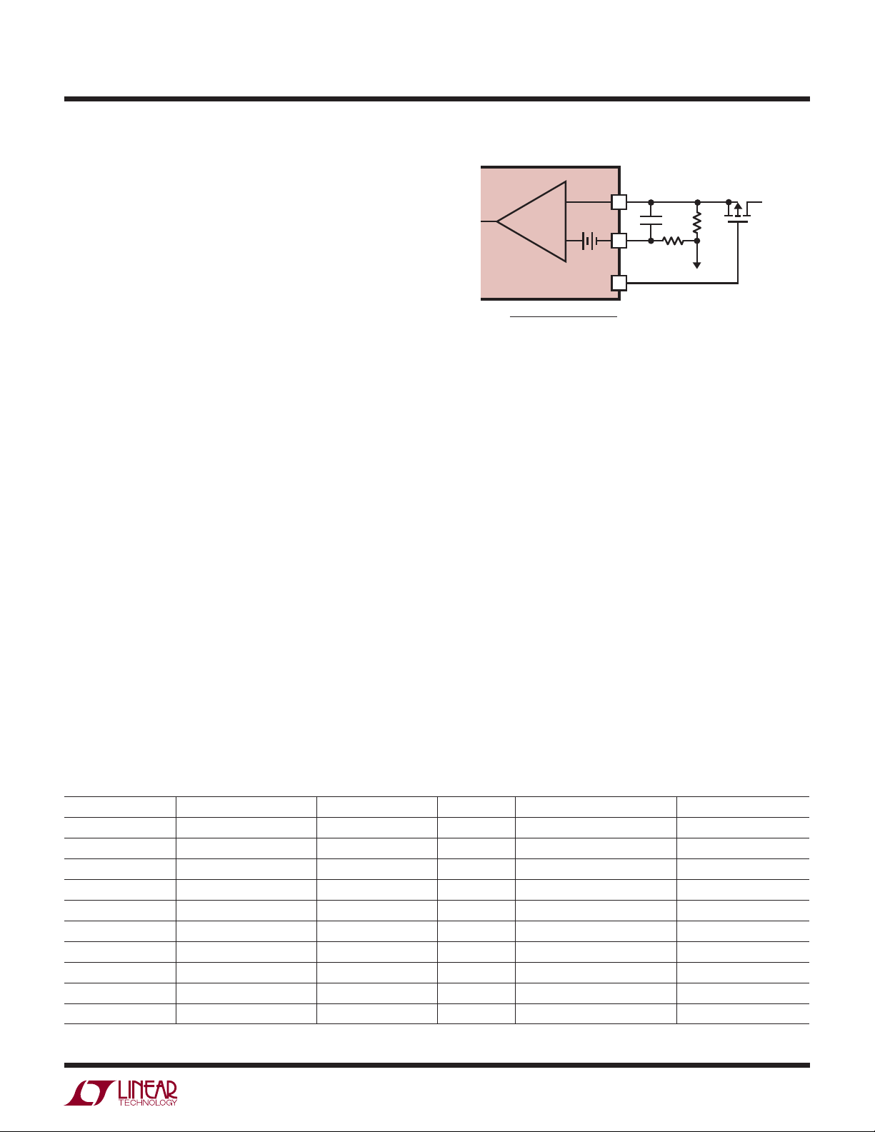
Adapter Limiting
An important feature of the LTC4100 is the ability to automatically adjust charging current to a level which avoids
overloading the wall adapter. This allows the product to
operate at the same time that batteries are being charged
without complex load management algorithms. Additionally, batteries will automatically be charged at the maximum
possible rate of which the adapter is capable.
This feature is created by sensing total adapter output
current and adjusting charging current downward if a
preset adapter current limit is exceeded. True analog
control is used, with closed loop feedback ensuring that
adapter load current remains within limits. Amplifi er CL1 in
Figure 9 senses the voltage across RCL, connected between the CLP and CLN pins. When this voltage exceeds
100mV, the amplifi er will override programmed charging
current to limit adapter current to 100mV/RCL. A lowpass
fi lter formed by 4.99k and 0.1µF is required to eliminate
switching noise. If the current limit is not used, CLP should
be connected to CLN.
Setting Input Current Limit
To set the input current limit, you need to know the minimum wall adapter current rating. Subtract 7% for the input
current limit tolerance and use that current to determine
the resistor value.
RCL = 100mV/I
I
= Adapter Min Current
LIM
– (Adapter Min Current • 7%)
LIM
LTC4100
LTC4100
–
CL1
+
+
100mV
*RCL =
100mV
ADAPTER CURRENT LIMIT
Figure 9. Adaptor Current Limiting
As is often the case, the wall adapter will usually have at
least a +10% current limit margin and many times one
can simply set the adapter current limit value to the actual
adapter rating (Figure 9).
Charge Termination Issues
Batteries with constant current charging and voltage-based
charger termination might experience problems with reductions of charger current caused by adapter limiting. It
is recommended that input limiting feature be defeated in
such cases. Consult the battery manufacturer for information on how your battery terminates charging.
Setting Output Current Limit (Refer to Figure 1)
The LTC4100 current DAC and the PWM analog circuitry
must coordinate the setting of the charger current. Failure
to do so will result in incorrect charge currents.
CLP
24
23
4
CLN
INFET
C9
0.1µF
R1
4.99k
RCL*
TO LOAD
4100 F09
V
IN
Table 8. Common RCL Resistor Values
ADAPTER RATING (A) –7% ADAPTER RATING (A) RCL VALUE* (Ω) 1% R
1.5 1.40 0.068 1.47 0.15 0.25
1.8 1.67 0.062 1.61 0.16 0.25
2.0 1.86 0.051 1.96 0.20 0.25
2.3 2.14 0.047 2.13 0.21 0.25
2.5 2.33 0.043 2.33 0.23 0.50
2.7 2.51 0.039 2.56 0.26 0.50
3.0 2.79 0.036 2.79 0.28 0.50
3.3 3.07 0.033 3.07 0.31 0.50
3.6 3.35 0.030 3.35 0.33 0.50
4.0 3.72 0.027 3.72 0.37 0.50
* Rounded to nearest 5% standard step value. Many non standard values are popular.
LIMIT (A) RCL POWER DISSIPATION (W) RCL POWER RATING (W)
CL
4100fb
21
Page 22
LTC4100
APPLICATIONS INFORMATION
I
is the full-scale charge current. Chose the lowest
MAX
value that is still above your expected battery charge
I
MAX
current as requested over the SMBus. If you deviate
from the resistance values shown in Table 9, it will lead
to charge current gain errors. The requested current and
the actual charge current applied to the battery will not
be the same.
Table 9. Recommended Resistor Values
I
(A) R
MAX
1.023 0.100 0.25 0
2.046 0.05 0.25 10k
3.068 0.025 0.5 33k
4.092 0.025 0.5 Open
Warning
DO NOT CHANGE THE VALUE OF R
TION. The value must remain fi xed and track the R
value at all times. Changing the current setting can result
in currents that greatly exceed the requested value and
potentially damage the battery or overload the wall adapter
if no input current limiting is provided.
Inductor Selection
Higher operating frequencies allow the use of smaller
inductor and capacitor values. A higher frequency generally results in lower effi ciency because of MOSFET gate
charge losses. In addition, the effect of inductor value
on ripple current and low current operation must also be
considered. The inductor ripple current ΔI
higher frequency and increases with higher V
ΔI
1
=
L OUT
fL
()()
Accepting larger values of ΔIL allows the use of low
inductances, but results in higher output voltage ripple
and greater core losses. A reasonable starting point for
setting ripple current is ΔI
maximum ΔI
L
inductor value also has an effect on low current operation.
(Ω) 1% R
SENSE
V
⎛
V
OUT
−
1
⎜
V
⎝
IN
= 0.4(I
L
SENSE
⎞
⎟
⎠
(W) R
ILIM
MAX
ILIM
DURING OPERA-
decreases with
L
.
IN
). Remember the
(Ω) 1%
SENSE
occurs at the maximum input voltage. The
The transition to low current operation begins when the
inductor current reaches zero while the bottom MOSFET
is on. Lower inductor values (higher ΔI
) will cause this
L
to occur at higher load currents, which can cause a dip in
effi ciency in the upper range of low current operation. In
practice 10µH is the lowest value recommended for use.
Table 10. Recommended Inductor Values
Maximum Average
Current (A) Input Voltage (V)
1 ≤20 40 ± 20%
1 >20 56 ± 20%
2 ≤20 20 ± 20%
2 >20 30 ± 20%
3 ≤20 15 ± 20%
3 >20 20 ± 20%
4 ≤20 10 ± 20%
4 >20 15 ± 20%
Minimum Inductor Value
(μH)
Charger Switching Power MOSFET
and Diode Selection
Two external power MOSFETs must be selected for use
with the charger: a P-channel MOSFET for the top (main)
switch and an N-channel MOSFET for the bottom (synchronous) switch.
The peak-to-peak gate drive levels are set internally. This
voltage is typically 6V. Consequently, logic-level threshold
MOSFETs must be used. Pay close attention to the BV
DSS
specifi cation for the MOSFETs as well; many of the logic
level MOSFETs are limited to 30V or less.
Selection criteria for the power MOSFETs include the
on-resistance R
transfer capacitance C
, total gate capacitance QG, reverse
DS(ON)
, input voltage and maximum
RSS
output current. The charger is operating in continuous
mode so the duty cycles for the top and bottom MOSFETs
are given by:
Main Switch Duty Cycle = V
OUT/VIN
Synchronous Switch Duty Cycle = (V
IN
– V
OUT
)/VIN
22
4100fb
Page 23

APPLICATIONS INFORMATION
LTC4100
The MOSFET power dissipations at maximum output
current are given by:
OUT
MAX
)/VIN(I
)2(1 + δΔT)R
)(C
)(f
RSS
OSC
)2(1 + δΔT)R
MAX
)
PMAIN = V
+ k(V
PSYNC = (V
OUT/VIN(IMAX
)2(I
IN
– V
IN
where δΔT is the temperature dependency of R
DS(ON)
DS(ON)
DS(ON)
and
k is a constant inversely related to the gate drive current.
2
Both MOSFETs have I
R losses while the PMAIN equation
includes an additional term for transition losses, which
are highest at high input voltages. For V
< 20V the high
IN
current effi ciency generally improves with larger MOSFETs,
while for V
the point that the use of a higher R
actually provides higher effi ciency. The synchronous
C
RSS
> 20V the transition losses rapidly increase to
IN
device with lower
DS(ON)
MOSFET losses are greatest at high input voltage or during
a short circuit when the duty cycle in this switch in nearly
100%. The term (1 + δΔT) is generally given for a MOSFET
in the form of a normalized R
vs temperature curve,
DS(ON)
but δ = 0.005/°C can be used as an approximation for low
voltage MOSFETs. C
= QGD/ΔVDS is usually specifi ed
RSS
in the MOSFET characteristics. The constant k = 2 can be
used to estimate the contributions of the two terms in the
main switch dissipation equation.
If the charger is to operate in low dropout mode or with
a high duty cycle greater than 85%, then the topside
P-channel effi ciency generally improves with a larger
MOSFET. Using asymmetrical MOSFETs may achieve cost
savings or effi ciency gains.
The Schottky diode D1, shown in the typical application
on the back page, conducts during the dead-time between
the conduction of the two power MOSFETs. This prevents
the body diode of the bottom MOSFET from turning on and
storing charge during the dead-time, which could cost as
much as 1% in effi ciency. A 1A Schottky is generally a good
size for 4A regulators due to the relatively small average
current. Larger diodes can result in additional transition
losses due to their larger junction capacitance.
Calculating IC Power Dissipation
The power dissipation of the LTC4100 is dependent upon
the gate charge of the top and bottom MOSFETs (Q2 &
Q3 respectively) The gate charge (QG) is determined from
the manufacturer’s data sheet and is dependent upon both
the gate voltage swing and the drain voltage swing of the
MOSFET. Use 6V for the gate voltage swing and V
DCIN
for
the drain voltage swing.
PD = V
Example: V
DCIN
• (f
QG
I
DD
(QGQ2 + QGQ3) + I
OSC
= 19V, f
DCIN
= 15nC, I
Q3
= 1mA.
) + VDD • I
DCIN
= 345kHz, QGQ2 = 25nC,
OSC
= 5mA, VDD = 5.5V,
DCIN
DD
PD = 428mW
Calculating V
The LTC4100 V
a. I
= Current due to active clocking and bias inside
RUN
Current
DD
current, or IDD, consist of three parts:
DD
the IC.
b. I
c. I
I
DD
a) I
= Current due to thermistor circuit activity.
THRM
= Current due to SMBus acceleration activity.
ACCEL
= I
+ I
RUN
current is basically independent of SCL clock rate.
RUN
THRM
+ I
ACCEL
Once the LTC4100 determines that there is activity on
the SMBus, it turns on its internal HF oscillator. This
HF oscillator remains on until a stop event occurs or
SDA and SCL are at logic level 1 for the SMBus timeout
period. Then it shuts off the HF oscillator. Thus, the
length of the transmission and the rate of transmission
bursts are more important in determining how much
current the LTC4100 burns, rather than the SCL rate.
In the equation below, I
consumes as a function of the V
is the static current the IC
Q
voltage when not
DD
active. Since it is hard to quantify the actual messages
going down the SMBus, one must estimate the SMBus
activity level in term of bus utilization per second.
The diode may be omitted if the effi ciency loss can be
tolerated.
= Message Duty Cycle • 950µA
I
RUN
+ (1 – Message Duty Cycle) • I
where IQ (typical) = VDD/47.2k
Q
4100fb
23
Page 24

LTC4100
APPLICATIONS INFORMATION
b) I
current is due to SafetySignal (thermistor pin)
THRM
sampling that will vary with the presence of DC power
being on or off. DCDIV is detected every 32ms. RTHX
is the value of the safety signal resistance, which will
vary with temperature or battery confi guration.
b1) I
THRM(ON)
I
THRM(ON)_OVERRANGE
when DC is on:
= 1/16 • VDD/(54.9k + RTHX)
where RTHX > 100k
I
THRM(ON)_COLD
= 1/8 • VDD/(54.9k + RTHX) where
RTHX > 30k
I
THRM(ON)_NORMAL
+ 1/16 • V
I
THRM(ON)_HOT
+ 1/8 • V
= 1/8 • VDD/(54.9k + RTHX)
/(1.13k + RTHX)
DD
* = 1/8 • VDD/(54.9k + RTHX)
/(1.13k + RTHX)
DD
where RTHX < 3k
*= includes underrange
b2) I
THRM(OFF)
when DC is off, the thermistor monitoring
rate is reduced to every 250ms or less.
c) I
is the current used by the SMBus accelerators.
ACCEL
This directly depends on the SMBus frequency, duty
cycle of messages sent on the SMBus and how long
it takes to drive the SMBus to V
I
ACCEL
= I
PULL-UP
• 2 • SMBus Frequency •
Message Duty Cycle• V
.
DD
/2.25V• Rise Time
DD
Complete Examples
1) Battery thermistor = 400Ω, V
= 5.0V
DD
Battery mode (DC is off), SMBus activity is 10kHz
and a 2% SMBus duty cycle, which represents a
suspended or sleep condition of a notebook.
= I
I
TOTAL
RUN
+ I
THRM(OFF)
+ I
ACCEL
= 121.9µA
+ 5.26µA + 2.44µA = 130µA
Battery mode and a 10% SMBus duty cycle, which
represents an active notebook at idle.
= I
I
TOTAL
RUN
+ I
THRM(OFF)
+ I
ACCEL
= 189.5µA
+ 5.26µA + 12.2µA = 207µA
I
THRM(OFF)_OVERRANGE
where RTHX > 100K
I
THRM(OFF)_COLD
+ 1/1000 • V
= 1/50 • VDD/(54.9k + RTHX)
/(54.9k + RTHX)
DD
where RTHX > 30K
I
THRM(OFF)_NORMAL
1/500 • V
DD
= 1/50 • VDD/(54.9k + RTHX) +
/(54.9k + RTHX) + 1/1000 • VDD/(1.13k
+ RTHX)
I
THRM(OFF)_HOT
1/500 • V
* = 1/50 • VDD/(54.9k + RTHX) +
/(54.9k + RTHX) + 1/500 • VDD/(1.13k +
DD
RTHX)
where RTHX < 3k
* includes underrange
= 1/50 • VDD/(54.9k + RTHX)
DCIN = ON and a 20% SMBus duty cycle which
represents an active notebook charging.
= I
I
TOTAL
RUN
+ I
THRM(ON)
+ I
ACCEL
= 274µA
+ 215.6µA + 24.4µA = 514µA
2) Battery thermistor = 10k, V
= 5.0V
DD
Battery mode (DC is off), SMBus activity is 10kHz
and a 2% SMBus duty cycle:
= I
I
TOTAL
RUN
+ I
THRM(OFF)
+ I
ACCEL
= 121.9µA
+ 2.14µA + 2.44µA = 126µA
Battery mode and a 10% SMBus duty cycle:
= I
I
TOTAL
RUN
+ I
THRM(OFF)
+ I
ACCEL
= 189.5µA
+ 2.14µA + 12.2µA = 204µA
DCIN = ON and a 20% SMBus duty cycle:
= I
I
TOTAL
RUN
+ I
THRM(OFF)
+ I
ACCEL
= 274µA
+ 37.7µA + 24.4µA = 336µA
24
4100fb
Page 25

APPLICATIONS INFORMATION
LTC4100
Soft-Start and Undervoltage Lockout
The LTC4100 is soft-started by the 0.12µF capacitor on
the I
to 0.5V, then ramp up at a rate set by the internal 30µA
pull-up current and the external capacitor. Battery charging
current starts ramping up when I
and full current is achieved with I
capacitor, time to reach full charge current is about 2ms and
it is assumed that input voltage to the charger will reach
full value in less than 2ms. The capacitor can be increased
up to 1µF if longer input start-up times are needed.
In any switching regulator, conventional timer-based
soft-starting can be defeated if the input voltage rises much
slower than the time out period. This happens because
the switching regulators in the battery charger and the
computer power supply are typically supplying a fi xed
amount of power to the load. If input voltage comes up
slowly compared to the soft-start time, the regulators will
try to deliver full power to the load when the input voltage
is still well below its fi nal value. If the adapter is current
limited, it cannot deliver full power at reduced output
voltages and the possibility exists for a quasi “latch” state
where the adapter output stays in a current limited state at
reduced output voltage. For instance, if maximum charger
plus computer load power is 30W, a 15V adapter might
be current limited at 2.5A. If adapter voltage is less than
(30W/2.5A = 12V) when full power is drawn, the adapter
voltage will be pulled down by the constant 30W load
until it reaches a lower stable state where the switching
regulators can no longer supply full load. This situation
can be prevented by utilizing the DCDIV resistor divider,
set higher than the minimum adapter voltage where full
power can be achieved.
pin. On start-up, ITH pin voltage will rise quickly
TH
voltage reaches 0.8V
TH
at 2V. With a 0.12µF
TH
into the charger or when a battery is connected to the
charger. Use only “surge robust” low ESR tantalums. Regardless of which type of capacitor you use, after voltage
selection, the most important thing to meet is the ripple
current requirements followed by the capacitance value.
By the time you solve the ripple current requirements,
the minimum capacitance value is often met by default.
The following equation shows the minimum C
tolerance) capacitance values for stability when used with
the compensation shown in the typical application on the
back page.
C
OUT(MIN)
The use of aluminum electrolytic for C1, located at the
AC adapter input terminal, is helpful in reducing ringing
during the hot-plug event. Refer to Application Note 88
for more information.
In the 4A lithium battery charger (typical application on
back page), the input capacitor (C2) is assumed to absorb
all input switching ripple current in the converter, so it
must have adequate ripple current rating. Worst-case RMS
ripple current will be equal to one half of output charging
current. C2 is recommended to be equal to or greater than
C4 (output capacitor) in capacitance value.
The output capacitor (C4) is also assumed to absorb
output switching current ripple. The general formula for
capacitor current is:
I
RMS
For example, V
f = 300kHz, I
= 200/L1
⎛
V
029 1
.•–
(
)
BAT
=
RMS
Lf
= 19V, V
DCIN
= 0.41A.
1
V
⎜
V
⎝
•
BAT
⎞
BAT
⎟
⎠
DCIN
= 12.6V, L1 = 10µH, and
OUT
(±20%
Input and Output Capacitors
We recommend the use of high capacity low ESR/ESL X5R
type ceramic capacitors. Alternative capacitors include
OSCON or POSCAP type capacitors. Aluminum electrolytic
capacitors are not recommended for poor ESR and ESL
reasons. Solid tantalum low ESR capacitors are acceptable,
but caution must be used when tantalum capacitors are
used for input or output bypass. High input surge currents
can be created when the power adapter is hot-plugged
EMI considerations usually make it desirable to minimize
ripple current in the battery leads, and beads or inductors may be added to increase battery impedance at the
300kHz switching frequency. Switching ripple current splits
between the battery and the output capacitor depending
on the ESR of the output capacitor and the battery impedance. If the ESR of C3
is raised to 4 with a bead or inductor, only 5% of the
current ripple will fl ow in the battery.
is 0.2 and the battery impedance
4100fb
25
Page 26
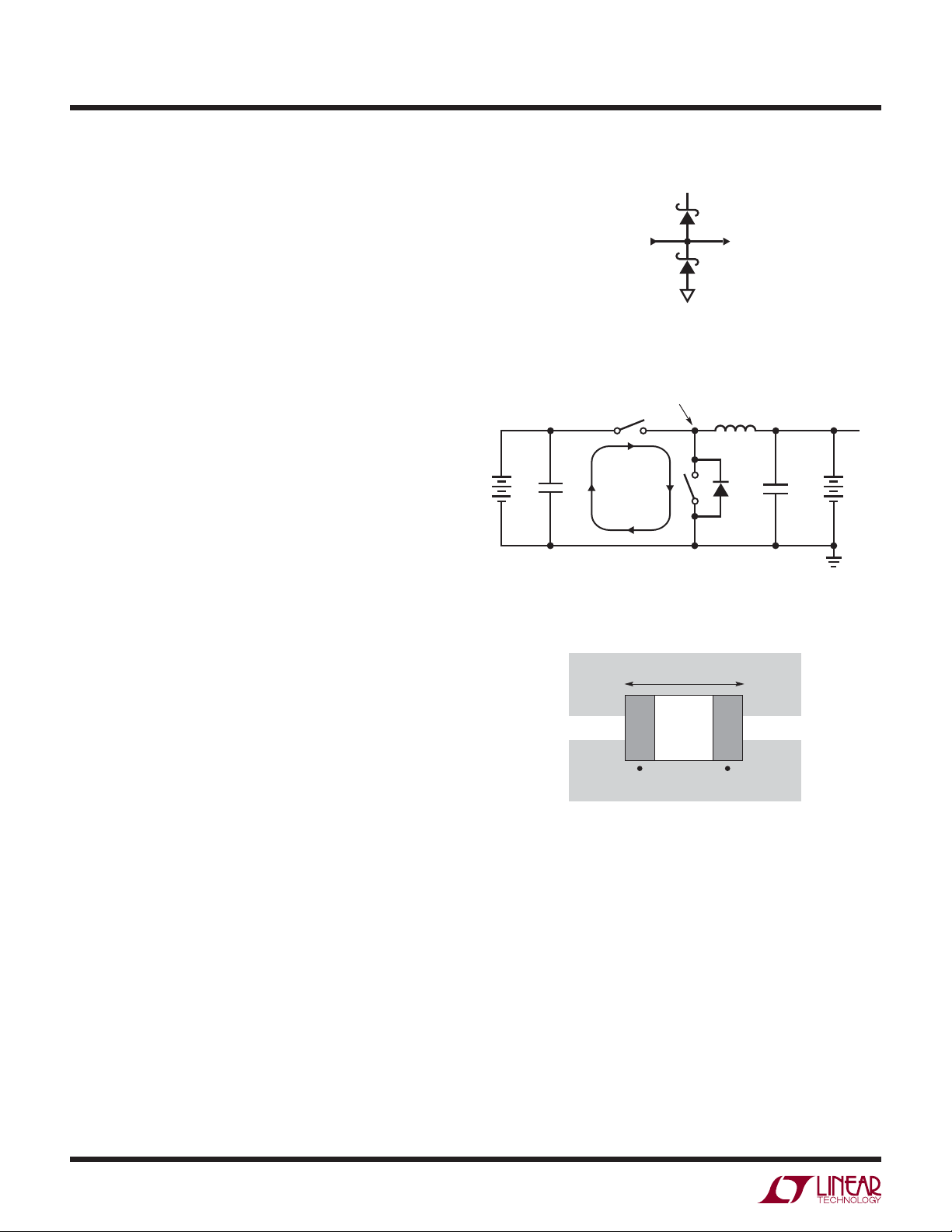
LTC4100
APPLICATIONS INFORMATION
Protecting SMBus Inputs
The SMBus inputs, SCL and SDA, are exposed to uncontrolled transient signals whenever a battery is connected
to the system. If the battery contains a static charge, the
SMBus inputs are subjected to transients which can cause
damage after repeated exposure. Also, if the battery’s positive terminal makes contact to the connector before the
negative terminal, the SMBus inputs can be forced below
ground with the full battery potential, causing a potential
for latch-up in any of the devices connected to the SMBus
inputs. Therefore it is good design practice to protect the
SMBus inputs as shown in Figure 10.
SafetySignal (Thermistor) Value
The SafetySignal (typical application on back page), is a
multifunction signal the communicates three pieces of
information in order of importance:
1) Presence of the Smart Battery
2) The maximum time duration of the wake-up charge
allowed.
V
DD
CONNECTOR
TO BATTERY
Figure 10. Recommended SMBus Transient Protection
SWITCH NODE
HIGH
FREQUENCY
V
C2
IN
CIRCULATING
PATH
Figure 11. High Speed Switching Path
TO SYSTEM
L1
D1
4100 F10
C4
BAT
4100 F11
V
BAT
3) An optional and redundant temperature measurement
system.
The value of the resistance to ground communicates all
this information. The resistance ranges and what it does
is covered by the SBS Smart Battery Charger standard in
Section 6. Basically if you have a battery chemistry, such
as Li-ion, that cannot safely withstand an infi nite duration wake-up charge, the SafetySignal resistance value
needs to be less than 425. The popular value to use is
a fi xed 300 resistor. Otherwise the resistance value is
10k which is normally expected to be done using a 10k
NTC resistor.
DIRECTION OF CHARGING CURRENT
R
SENSE
VIAS TO CSP AND BAT
4100 F12
Figure 12. Kelvin Sensing of Charging Current
26
4100fb
Page 27

APPLICATIONS INFORMATION
LTC4100
PCB Layout Considerations
For maximum effi ciency, the switch node rise and fall times
should be minimized. To prevent magnetic and electrical fi eld
radiation and high frequency resonant problems, proper
layout of the components connected to the IC is essential.
(See Figure 11.) Here is a PCB layout priority list for proper
layout. Layout the PCB using this specifi c order.
1. Input capacitors need to be placed as close as possible
to switching FET’s supply and ground connections.
Shortest copper trace connections possible. These
parts must be on the same layer of copper. Vias must
not be used to make this connection.
2. The control IC needs to be close to the switching FET’s
gate terminals. Keep the gate drive signals short for
a clean FET drive. This includes IC supply pins that
connect to the switching FET source pins. The IC can
be placed on the opposite side of the PCB relative to
above.
3. Place inductor input as close as possible to switching
FET’s output connection. Minimize the surface area of
this trace. Make the trace width the minimum amount
needed to support current—no copper fi lls or pours.
Avoid running the connection using multiple layers in
parallel. Minimize capacitance from this node to any
other trace or plane.
4. Place the output current sense resistor right next to
the inductor output but oriented such that the IC’s
current sense feedback traces going to resistor are not
long. The feedback traces need to be routed together
as a single pair on the same layer at any given time
with smallest trace spacing possible. Locate any fi lter
component on these traces next to the IC and not at
the sense resistor location.
5. Place output capacitors next to the sense resistor
output and ground.
6. Output capacitor ground connections need to feed
into same copper that connects to the input capacitor
ground before tying back into system ground.
Interfacing with a Selector
The LTC4100 is designed to be used with a true analog
multiplexer for the SafetySignal sensing path. Some
selector ICs from various manufacturers may not implement this. Consult LTC applications department for more
information.
Electronic Loads
The LTC4100 is designed to work with a real battery.
Electronic loads will create instability within the LTC4100
preventing accurate programming currents and voltages. Consult LTC applications department for more
information.
4100fb
27
Page 28
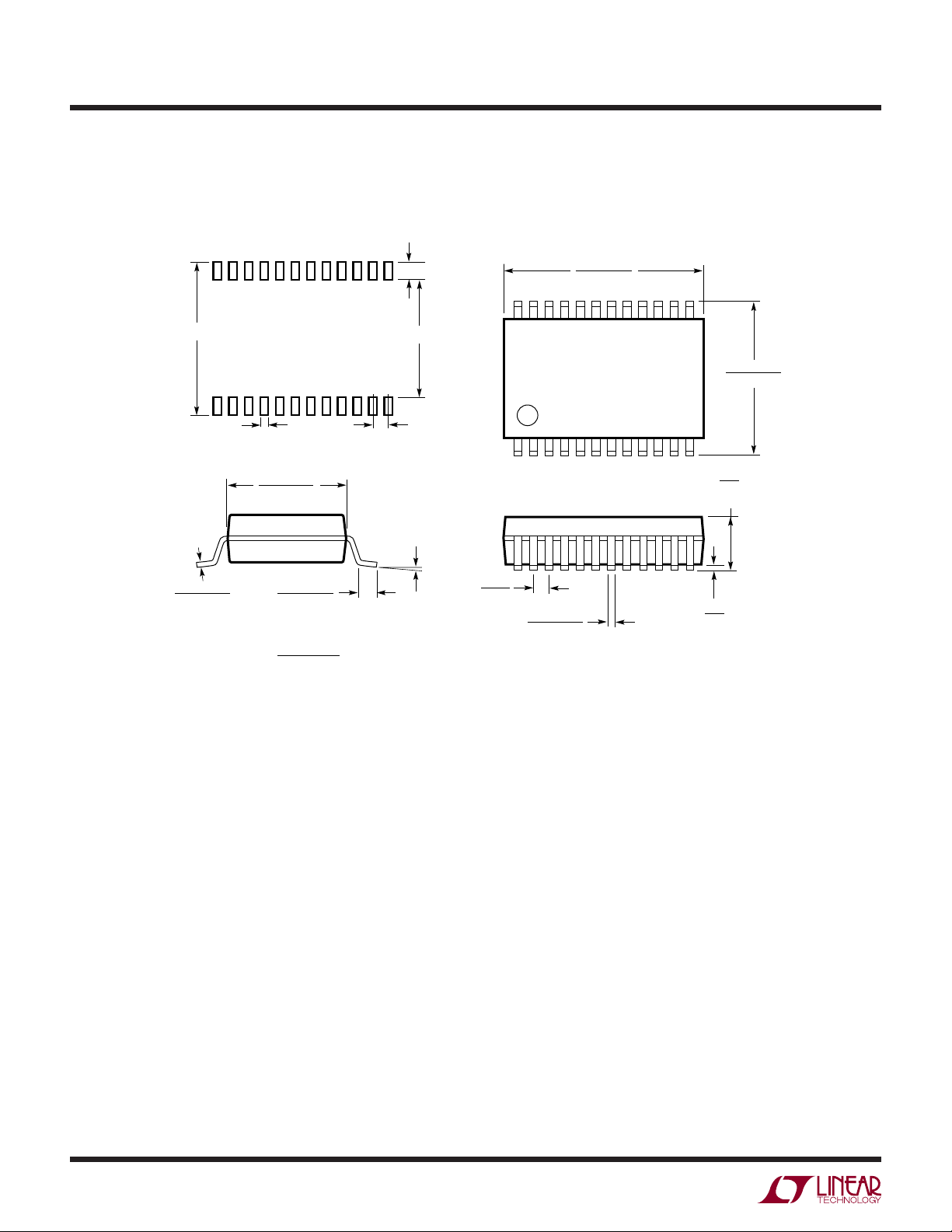
LTC4100
PACKAGE DESCRIPTION
G Package
24-Lead Plastic SSOP (5.3mm)
(Reference LTC DWG # 05-08-1640)
1.25 ±0.12
7.8 – 8.2
0.42 ±0.03 0.65 BSC
RECOMMENDED SOLDER PAD LAYOUT
5.00 – 5.60**
(.197 – .221)
0.09 – 0.25
(.0035 – .010)
NOTE:
1. CONTROLLING DIMENSION: MILLIMETERS
2. DIMENSIONS ARE IN
3. DRAWING NOT TO SCALE
*
DIMENSIONS DO NOT INCLUDE MOLD FLASH. MOLD FLASH
SHALL NOT EXCEED .152mm (.006") PER SIDE
**
DIMENSIONS DO NOT INCLUDE INTERLEAD FLASH. INTERLEAD
FLASH SHALL NOT EXCEED .254mm (.010") PER SIDE
0.55 – 0.95
(.022 – .037)
MILLIMETERS
(INCHES)
5.3 – 5.7
0° – 8°
7.90 – 8.50*
(.311 – .335)
2122 18 17 16 15 14
19202324
12345678 9 10 11 12
0.65
(.0256)
BSC
0.22 – 0.38
(.009 – .015)
TYP
13
(.291 – .323)
2.0
(.079)
MAX
0.05
(.002)
MIN
G24 SSOP 0204
7.40 – 8.20
28
4100fb
Page 29
LTC4100
REVISION HISTORY
REV DATE DESCRIPTION PAGE NUMBER
B 10/09 Add Table to Typical Application
Text Added to Pin Functions
Text Changes to Operation Section
Changes to Table 1
Added ‘Calculating V
Updated ‘Input and Output Capacitors’ Section
Added ‘SafetySignal (Thermistor) Value’ Section
Changes to Typical Application
(Revision history begins at Rev B)
Current’ Section
DD
1
8
11, 12, 15
13
23
25
26
29
Information furnished by Linear Technology Corporation is believed to be accurate and reliable.
However, no responsibility is assumed for its use. Linear Technology Corporation makes no representation that the interconnection of its circuits as described herein will not infringe on existing patent rights.
4100fb
29
Page 30
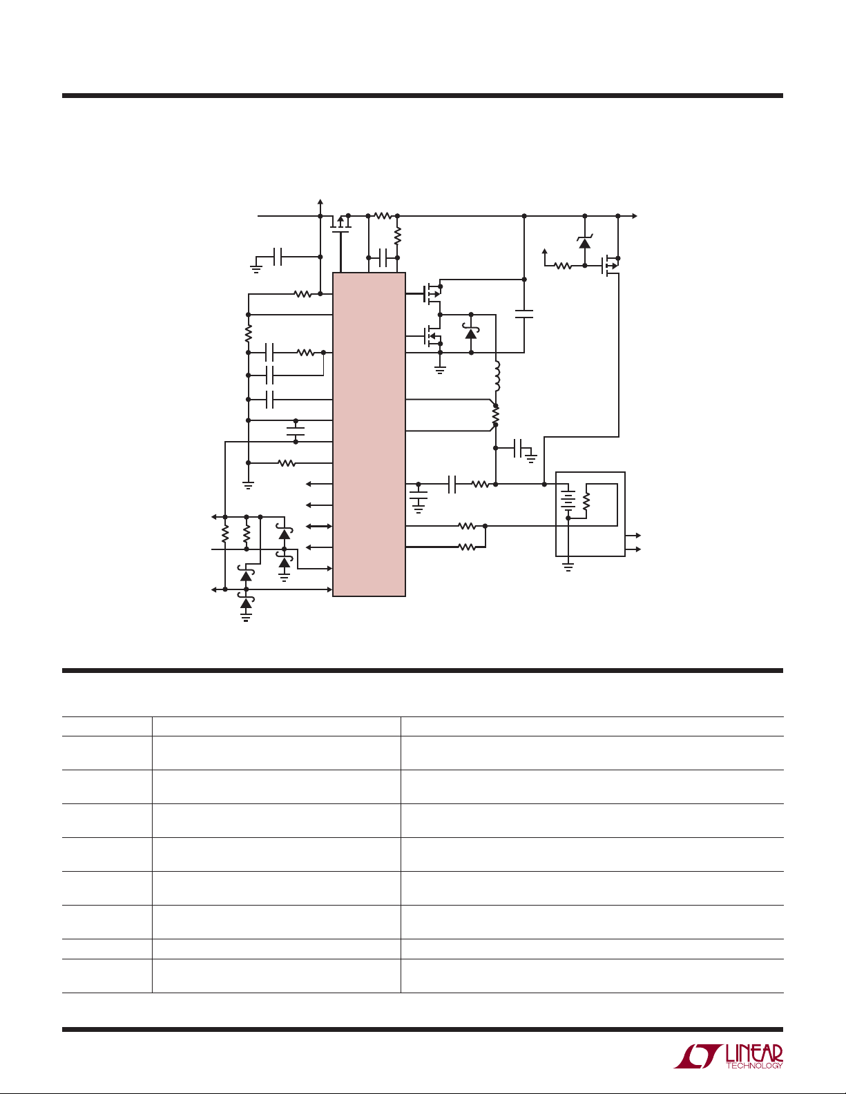
LTC4100
TYPICAL APPLICATION
3V TO 5.5V
SDA
SCL
LTC4100 Li-Ion Battery Charger I
R
CL
0.033
0.5W
1%
Q1
C9
0.1µF
10V
424 23
INFET
DCIN
DCDIV
I
TH
I
DC
GND
V
V
I
LIM
ACP
CHGEN
SMBALERT
SDA
SCL
TGATE
BGATE
LTC4100
DD
LIM
15V TO 20V
DCIN
FROM WALL
ADAPTER
R11
1.21k
1%
10k10k
D4
D5
C1
0.1µF
C6, 0.12µF
10V, X7R
C7, 0.0015µF
10V, X7R
C8, 0.068µF
10V, X7R
0.1µF
10V
R6, R
VLIM
D2
D3
R10
13.7k
1%
6.04k
1%
33k
DCIN
5
11
R5
19
20
12
17
14
13
10
6
7
8
9
= 4A/V
LIM
CLNCLP
PGND
CSP
BAT
V
SET
THA
THB
4100 TA02
LIM
R1
4.9k
1
Q2
3
Q3
2
21
22
C4
0.01µF
25V
18
C5
0.1µF
10V
16
15
D1: MBRM140T3G
D2-D5: SMALL SIGNAL SCHOTTKY
D6: 18V ZENER DIODE
Q1: 1/2 Si4925BDY
Q2: FDS6685
Q3: FDC645N
Q4: 1/2 Si4925
= 17.4V, Adapter Rating = 2.7A
D6
100k
4-CELL Li-Ion
SMART BATTERY
300
R
SNS
0.025
0.5W, 1%
R4
100
R
THA
1.13k
1%
R
THB
54.9k
1%
D1
L1
10µH
4A
C4,C5
10µF s2
25V
X5R
SafetySignal
DCIN
C2, C3
10µF s2
25V
X5R
SYSTEM
LOAD
Q4
OPTIONAL
DISCHARGE
PATH TO
SYSTEM
LOAD
SDA
SCL
RELATED PARTS
PART NUMBER DESCRIPTION COMMENTS
LTC1760 Smart Battery System Manager Autonomous Power Management and Battery Charging for Two Smart Batteries,
LTC1960 Dual Battery Charger/Selector with SPI Interface Simultaneous Charge or Discharge of 2 Batteries, DAC Programmable Current
LTC1980 Combination Battery Charger and DC/DC Converter Input Supply May be Above or Below Battery Voltage, up to 8.4V Float Voltage,
LTC4006 Small, High Effi ciency, Fixed Voltage, Lithium-Ion
Battery Charger
LTC4007 High Effi ciency, Programmable Voltage Battery
Charger with Termination
LTC4008 High Effi ciency, Programmable Voltage/Current
Battery Charger
LTC4101 Smart Battery Charger Controller For Smart Batteries with Voltages Below 5.5V
LTC4412 Low Loss PowerPath™ Controller Very Low Loss Replacement for Power Supply OR’ing Diodes Using Minimal
PowerPath is a trademark of Linear Technology Corporation.
Linear Technology Corporation
30
1630 McCarthy Blvd., Milpitas, CA 95035-7417
(408) 432-1900 ● FAX: (408) 434-0507
●
www.linear.com
SMBus Rev 1.1 Compliant
and Voltage, Input Current Limiting Maximizes Charge Current
24-Pin SSOP Package
Constant Current/Constant Voltage Switching Regulator with Termination Timer,
AC Adapter Current Limit and SafetySignal Sensor in a Small 16-Pin Package
Complete Charger for 3- or 4-Cell Li-Ion Batteries, AC Adapter Current Limit,
SafetySignal Sensor and Indicator Outputs
Constant Current/Constant Voltage Switching Regulator; Resistor Voltage/
Current Programming, AC Adapter Current Limit and SafetySignal Sensor
External Components
4100fb
LT 1109 REV B • PRINTED IN USA
© LINEAR TECHNOLOGY CORPORATION 2006
 Loading...