

Page 1
LTC4089/LTC4089-5
1
40895fb
HVIN
BOOST
HVEN
IN
SW
4.7µF
10µF
4.7µF
1µF
TIMER
CLPROG
LTC4089
GND PROG
HVOUT
HVPR
OUT
BAT
0.1µF
100k2k
5V (NOM)
FROM USB
CABLE V
BUS
HIGH (6V-36V)
VOLTAGE INPUT
Li-Ion BATTERY
+
1k
TO LDOs
R
EGS
, ETC.
4089 TAO1
VOUT (TYP)
V
BAT
+0.3V
5V
5V
V
BAT
AVAILABLE INPUT
HV INPUT (LTC4089)
HV INPUT (LTC4089-5)
USB ONLY
BAT ONLY
10µH
0.1µF
, LT, LTC and LTM are registered trademarks of Linear Technology Corporation.
All other
trademarks are the property of their respective owners.
Burst Mode is a registered trademark
of Linear Technology Corporation.
Protected by U.S. Patents including 6522118 and 6700364.
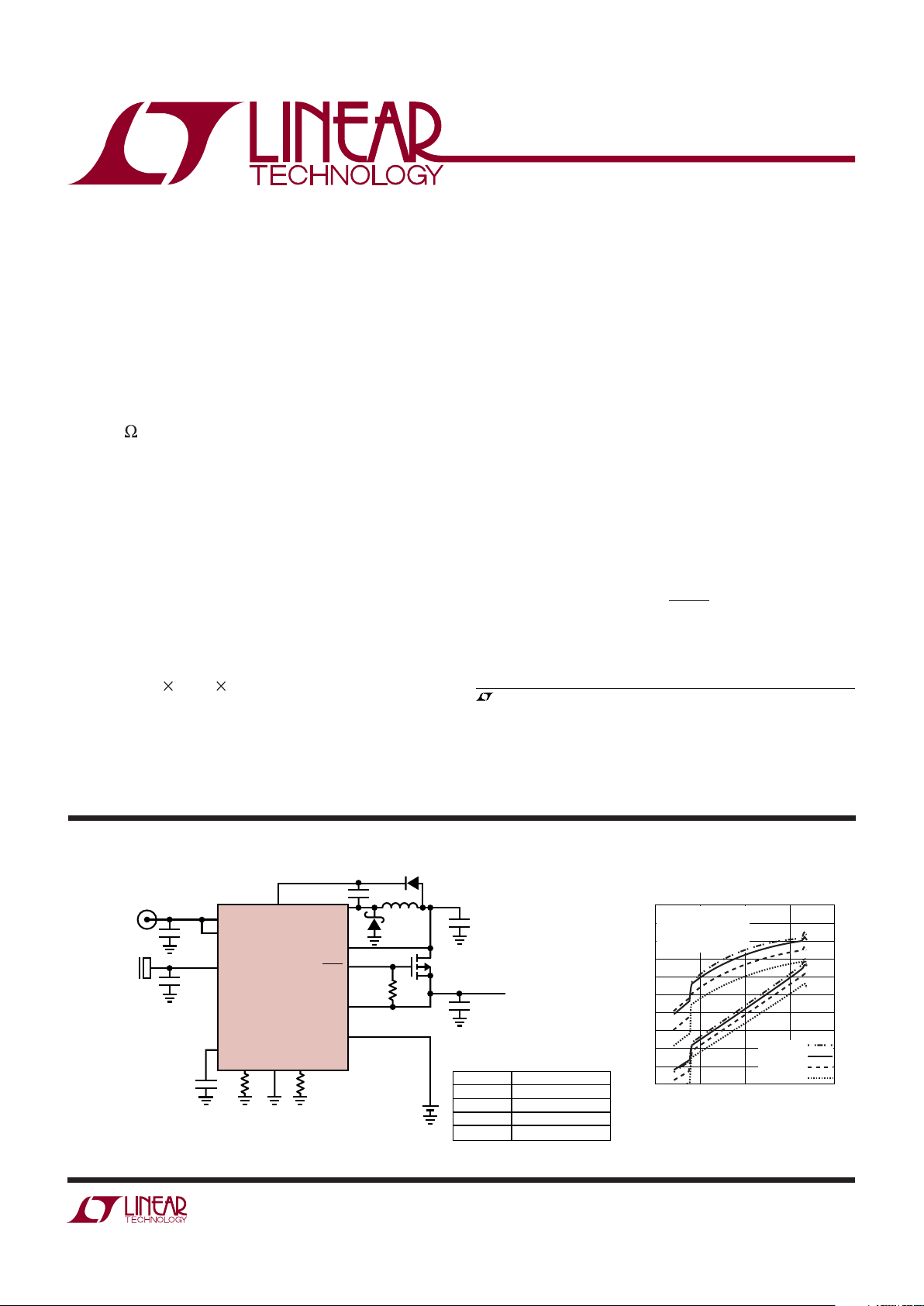
TYPICAL APPLICATIO
U
USB Power Manager with
High Voltage Switching Charger
The LTC®4089/LTC4089-5 are USB power managers plus
high voltage Li-Ion battery chargers. These devices control
the total current used by the USB peripheral for operation
and battery charging. Battery charge current is automatically reduced such that the sum of the load current and
the charge current does not exceed the programmed input
current limit. The LTC4089/LTC4089-5 also accommodate
high voltage power supplies, such as 12V AC-DC wall
adapters, FireWire, or automotive power.
The LTC4089 provides an adaptive output that tracks the
battery voltage for high effi ciency charging from the high
voltage input. The LTC4089-5 provides a fi xed 5V output
from the high voltage input to charge single cell Li-Ion
batteries. The charge current is programmable and an
end-of-charge status output (CHRG) indicates full charge.
Also featured is programmable total charge time, an NTC
thermistor input used to monitor battery temperature while
charging and automatic recharging of the battery.
■
Portable USB Devices—GPS Receivers, Cameras,
MP3 Players, PDAs
■
Seamless Transition Between Power Sources: Li-Ion
Battery, USB, and 6V to 36V External Supply
■
High Effi ciency 1.2A Charger from 6V to 36V Input
with Adaptive Output Control (LTC4089)
■
Load Dependent Charging from USB Input
Guarantees Current Compliance
■
215m Internal Ideal Diode plus Optional External
Ideal Diode Controller Provides Low Loss Power
Path When External Supply/USB Not Present
■
Constant-Current/Constant-Voltage Operation with
Thermal Feedback to Maximize Charging Rate
without Risk of Overheating
■
Selectable 100% or 20% Current Limit (e.g., 500mA/
100mA) from USB Input
■
Preset 4.2V Charge Voltage with 0.8% Accuracy
■
C/10 Charge Current Detection Output
■
NTC Thermistor Input for Temperature Qualifi ed
Charging
■
Tiny (6mm 3mm 0.75mm) 22-Pin DFN Package
APPLICATIO S
U
FEATURES
DESCRIPTIO
U
LTC4089 High Voltage
Battery Charger Effi ciency
BATTERY VOLTAGE (V)
2.5
40
EFFICIENCY (%)
45
55
60
65
90
75
3
3.5
4089 TA01b
50
80
85
70
4
4.5
HVIN = 8V
HVIN = 12V
HVIN = 24V
HVIN = 36V
CC CURRENT = 970mA
NO OUTPUT LOAD
FIGURE 10 SCHEMATIC
WITH R
PROG
= 52k
LTC4089-5
LTC4089
Page 2
LTC4089/LTC4089-5
2
40895fb
Terminal Voltage
BOOST ...................................................... –0.3V to 50V
BOOST above SW .....................................................25V
HVIN, HVEN .............................................. –0.3V to 40V
IN, OUT, HVOUT
t < 1ms and Duty Cycle < 1% .................. –0.3V to 7V
DC ............................................................ –0.3V to 6V
BAT .............................................................. –0.3V to 6V
NTC, TIMER, PROG, CLPROG .......–0.3V to (V
CC
+ 0.3V)
CHRG, HPWR, SUSP, HVPR ......................... –0.3V to 6V
Pin Current, DC
IN, OUT, BAT (Note 6) ..............................................2.5A
Operating Temperature Range
LTC4089E ................................................. –40°C to 85°C
Maximum Operating Junction Temperature .......... 110°C
Storage Temperature Range ................... –65°C to 125°C
(Notes 1, 2, 3, 4, 5)
The
● denotes the specifi cations which apply over the full operating
temperature range, otherwise specifi cations are at TA = 25°C. HVIN = 12V, BOOST = 17V, VIN = 5V, V
BAT
= 3.7V, HVEN = 12V,
HPWR = 5V, R
PROG
= 100k, R
CLPROG
= 2k, SUSP = 0V, unless otherwise noted.
SYMBOL PARAMETER CONDITIONS MIN TYP MAX UNITS
USB Input Current Limit
V
IN
USB Input Supply Voltage IN
●
4.35 5.5 V
I
IN
Input Bias Current I
BAT
= 0 (Note 7)
Suspend Mode; SUSP = 5V
●
●
0.5
50
1
100
mA
µA
I
LIM
Current Limit R
CLPROG
= 2k, HPWR = 5V
R
CLPROG
= 2k, HPWR = 0V
●
●
475
90
500
100
525
110
mA
mA
I
IN(MAX)
Maximum Input Current Limit (Note 8) 2.4 A
R
ON
ON Resistance VIN to V
OUT
I
OUT
= 80mA Load 0.215
V
CLPROG
CLPROG Pin Voltage R
CLPROG
= 2k
R
CLPROG
= 1k
●
●
0.98
0.98
1.00
1.00
1.02
1.02
V
V
I
SS
Soft-Start Inrush Current IN 5 mA/µs
V
CLEN
Input Current Limit Enable
Threshold Voltage (V
IN
– V
OUT
)
(V
IN
– V
OUT
) VIN Rising
(V
IN
– V
OUT
) VIN Falling
20
–80
50
–50
80
–20
mV
mV
ELECTRICAL CHARACTERISTICS
ABSOLUTE AXI U RATI GS
W
WW
U
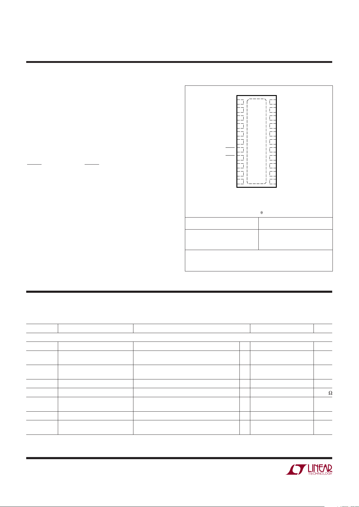
PACKAGE/ORDER I FOR ATIO
UUW
22
21
20
19
18
17
16
15
14
13
12
1
2
3
4
5
6
7
8
9
10
11
HVEN
HVIN
BOOST
SW
HVOUT
TIMER
SUSP
HPWR
CLPROG
OUT
IN
TOP VIEW
23
DJC PACKAGE
22-LEAD (6mm × 3mm) PLASTIC DFN
GND
GND
HVOUT
V
C
NTC
VNTC
HVPR
CHRG
PROG
GATE
BAT
EXPOSED PAD (PIN 23) IS GND
(MUST BE SOLDERED TO PCB)
T
JMAX
= 110°C, JA = 40°C/W
ORDER PART NUMBER DJC PART MARKING
LTC4089EDJC
LTC4089EDJC-5
4089
40895
Order Options Tape and Reel: Add #TR
Lead Free: Add #PBF Lead Free Tape and Reel: Add #TRPBF
Lead Free Part Marking: http://www.linear.com/leadfree/
Consult LTC Marketing for parts specifi ed with wider operating temperature ranges.
Page 3
LTC4089/LTC4089-5
3
40895fb
SYMBOL PARAMETER CONDITIONS MIN TYP MAX UNITS
V
UVLO
Input Undervoltage Lockout VIN Powers Part, Rising Threshold
●
3.6 3.8 4 V
dV
UVLO
Input Undervoltage Lockout
Hysteresis
VIN Rising – VIN Falling 130 mV
High Voltage Regulator
V
HVIN
HVIN Supply Voltage 6 36 V
I
HVIN
HVIN Bias Current Not Switching
Shutdown; HVEN = 0V
1.9
0.01
2.5
2
mA
µA
V
OUT
Output Voltage with HVIN Present Assumes HVOUT to OUT Connection (LTC4089)
Assumes HVOUT to OUT Connection (LTC4089-5)
●
3.45
4.85
V
BAT
+0.354.6
5.15
V
V
V
HVUVLO
High Voltage Input Undervoltage
Lockout
V
HVIN
Rising 4.7 5 V
f
SW
Switching Frequency V
HVOUT
> 3.95V
V
HVOUT
= 0V
685 750
35
815 kHz
kHz
DC
MAX
Maximum Duty Cycle
●
88 95 %
I
SW(MAX)
Switch Current Limit (Note 9) 1.5 1.95 2.3 A
V
SAT
Switch V
CESAT
ISW = 1A 330 mV
I
LK
Switch Leakage Current 2µA
V
SWD
Minimum Boost Voltage Above SW ISW = 1A 1.85 2.2 V
I
BST
BOOST Pin Current ISW = 1A 30 50 mA
Battery Management
V
BAT
Input Voltage BAT 4.3 V
I
BAT
Battery Drain Current V
BAT
= 4.3V, Charging Stopped
Suspend Mode; SUSP = 5V
V
HVIN
= VIN = 0V, BAT Powers OUT, No Load
●
●
●
15
22
60
27
35
100
µA
µA
µA
V
FLOAT
Regulated Output Voltage I
BAT
= 2mA
I
BAT
= 2mA; (0°C – 85°C)
4.165
4.158
4.200
4.200
4.235
4.242
V
V
I
CHG
Current Mode Charge Current R
PROG
= 100k, No Load
R
PROG
= 50k, No Load; (0°C – 85°C)
●
465
900
500
1000
535
1080
mA
mA
I
CHG(MAX)
Maximum Charge Current (Note 8) 1.2 A
V
PROG
PROG Pin Voltage R
PROG
= 100k
R
PROG
= 50k
●
●
0.98
0.98
1.00
1.00
1.02
1.02
V
V
k
EOC
Ratio of End-of-Charge Current to
Charge Current
V
BAT
= V
FLOAT
(4.2V)
●
0.085 0.1 0.11 mA/mA
I
TRIKL
Trickle Charge Current V
BAT
= 2V, R
PROG
= 100k 35 50 60 mA
V
TRIKL
Trickle Charge Threshold Voltage
●
2.75 2.9 3 V
V
CEN
Charger Enable Threshold Voltage (V
OUT
– V
BAT
) Falling; V
BAT
= 4V
(V
OUT
– V
BAT
) Rising; V
BAT
= 4V
55
80
mV
mV
V
RECHRG
Recharge Battery Threshold Voltage V
FLOAT
- V
RECHRG
●
65 100 135 mV
t
TIMER
TIMER Accuracy V
BAT
= 4.3V –10 10 %
Recharge Time Percent of Total Charge Time 50 %
Low Battery Trickle Charge Time Percent of Total Charge Time, V
BAT
< 2.8V 25 %
T
LIM
Junction Temperature in Constant
Temperature Mode
105 °C
The ● denotes the specifi cations which apply over the full operating
temperature range, otherwise specifi cations are at T
A
= 25°C. HVIN = 12V, BOOST = 17V, VIN = 5V, V
BAT
= 3.7V, HVEN = 12V,
HPWR = 5V, R
PROG
= 100k, R
CLPROG
= 2k, SUSP = 0V, unless otherwise noted.
ELECTRICAL CHARACTERISTICS
Page 4
LTC4089/LTC4089-5
4
40895fb
SYMBOL PARAMETER CONDITIONS MIN TYP MAX UNITS
Internal Ideal Diode
R
FWD
Incremental Resistance, VON
Regulation
I
BAT
= 100mA 125
m
R
DIO,ON
ON Resistance V
BAT
to V
OUT
I
BAT
= 600mA 215
m
V
FWD
Voltage Forward Drop (V
BAT
- V
OUT
)I
BAT
= 5mA
I
BAT
= 100mA
I
BAT
= 600mA
●
10 30
55
160
50 mV
mV
mV
V
OFF
Diode Disable Battery Voltage 2.8 V
I
FWD
Load Current Limit, for VON
Regulation
550 mA
I
D(MAX)
Diode Current Limit 2.2 A
External Ideal Diode
V
FWD, EXT
External Diode Forward Voltage 20 mV
Logic
V
OL
Output Low Voltage (CHRG, HVPR) I
SINK
= 5mA
●
0.1 0.4 V
V
IH
Input High Voltage HVEN, SUSP, HPWR Pin Low to High 2.3 V
V
IL
Input Low Voltage HVEN, SUSP, HPWR Pin High to Low 0.3 V
I
PULLDN
Logic Input Pull Down Current SUSP, HPWR 2 µA
I
HVEN
HVEN Pin Bias Current V
HVEN
= 2.3V
V
HVEN
= 0V
6
0.01
20
0.1
µA
µA
V
CHG,SD
Charger Shutdown Threshold
Voltage on TIMER
●
0.14 0.4 V
I
CHG,SD
Charger Shutdown Pull-Up Current
on TIMER
V
TIMER
= 0V
●
514 µA
NTC
I
VNTC
VNTC Pin Current V
VNTC
= 2.5V
●
1.4 2.5 3.5 mA
V
VNTC
VNTC Bias Voltage I
VNTC
= 500µA
●
4.4 4.85 V
I
NTC
NTC Input Leakage Current V
NTC
= 1V 0
±1
µA
V
COLD
Cold Temperature Fault Threshold
Voltage
Rising Threshold
Hysteresis
0.74•V
VNTC
0.02•V
VNTC
V
V
V
HOT
Hot Temperature Fault Threshold
Voltage
Falling Threshold
Hysteresis
0.29•V
VNTC
0.01•V
VNTC
V
V
V
DIS
NTC Disable Voltage NTC Input Voltage to GND (Falling)
Hysteresis
●
75 100
35
125 mV
mV
The ● denotes the specifi cations which apply over the full operating
temperature range, otherwise specifi cations are at T
A
= 25°C. HVIN = 12V, BOOST = 17V, VIN = 5V, V
BAT
= 3.7V, HVEN = 12V,
HPWR = 5V, R
PROG
= 100k, R
CLPROG
= 2k, SUSP = 0V, unless otherwise noted.
ELECTRICAL CHARACTERISTICS
Note 1: Stresses beyond those listed under Absolute Maximum Ratings
may cause permanent damage to the device. Exposure to any Absolute
Maximum Rating condition for extended periods may affect device
reliability and lifetime.
Note 2: V
CC
is the greater of VIN, V
OUT
or V
BAT
Note 3: All voltage values are with respect to GND.
Note 4: This IC includes over-temperature protection that is intended
to protect the device during momentary overload conditions. Junction
temperatures will exceed 110°C when over-temperature protection is
active. Continuous operation above the specifi ed maximum operating
junction temperature may result in device degradation or failure.
Note 5: The LTC4089/LTC4089-5 are guaranteed to meet specifi ed
performance from 0°C to 85°C and are designed, characterized and
expected to meet these extended temperature limits, but are not tested
at –40°C and 85°C.
Note 6: Guaranteed by long term current density limitations.
Note 7: Total input current is equal to this specifi cation plus 1.002 • I
BAT
where I
BAT
is the charge current.
Note 8: Accuracy of programmed current may degrade for currents greater
than 1.5A.
Note 9: Current limit guaranteed by design and/or correlation to static test.
Slope compensation reduces current limit at high duty cycle.
Page 5
LTC4089/LTC4089-5
5
40895fb
TIME (MIN)
0
V
BAT
, V
OUT
, V
CHRGB
(V)
I
BAT
(mA)
2
3
200
40895 G03
1
0
50
100
150
5
4
600
900
300
0
1500
1200
V
BAT
V
OUT
V
CHRGB
I
BAT
1250mAh
CELL
HVIN = 12V
R
PROG
= 50k
C/10
TERMINATION
I
BAT
(mA)
0
4.00
V
FLOAT
(V)
4.05
4.10
4.15
4.20
4.25
4.30
200 400 600 800
40895 G01
1000
R
PROG
= 34k
TEMPERATURE (°C)
–50
V
FLOAT
(V)
4.195
4.200
4.205
25
75
40895 G02
4.190
4.185
4.180
–25 0 50
4.210
4.215
4.220
100
VIN = 5V
I
BAT
= 2mA
V
BAT
(V)
0
0
I
BAT
(mA)
100
300
400
500
1
2
2.5 4.5
40895 G04
200
0.5 1.5
3
3.5
4
600
VIN = 5V
V
OUT
= NO LOAD
R
PROG
= 100k
R
CLPROG
= 2k
HPWR = 5V
HPWR = 0V
TEMPERATURE (°C)
–50
I
BAT
(mA)
400
500
600
25 75
40895 G05
300
200
–25 0
50 100 125
100
0
VIN = 5V
V
BAT
= 3.5V
θ
JA
= 50°C/W
V
FWD
(mV)
0
0
I
OUT
(mA)
100
300
400
500
1000
700
50
100
40895 G06
200
800
900
600
150
200
V
BAT
= 3.7V
V
IN
= 0V
–50°C
0°C
50°C
100°C
0
3000
4000
5000
80
4085 G17
2000
1000
2500
3500
4500
1500
500
0
20
40
60
100
V
FWD
(mV)
I
OUT
(mA)
V
BAT
= 3.7V
V
IN
= 0V
Si2333 PFET
–50°C
0°C
50°C
100°C
I
OUT
(A)
0
EFFICIENCY (%)
80
90
100
0.8
40895 G08
70
60
75
85
95
65
55
50
0.2
0.4
0.6
1.0
FIGURE 10 SCHEMATIC
V
BAT
= 4.21V (I
BAT
= 0)
HVIN = 8V
HVIN = 12V
HVIN = 36V
HVIN = 24V
I
OUT
(A)
0
EFFICIENCY (%)
80
90
100
0.8
40895 G09
70
60
75
85
95
65
55
50
0.2
0.4
0.6
1.0
FIGURE 10 SCHEMATIC
V
BAT
= 4.21V (I
BAT
= 0)
HVIN = 8V
HVIN = 12V
HVIN = 36V
HVIN = 24V
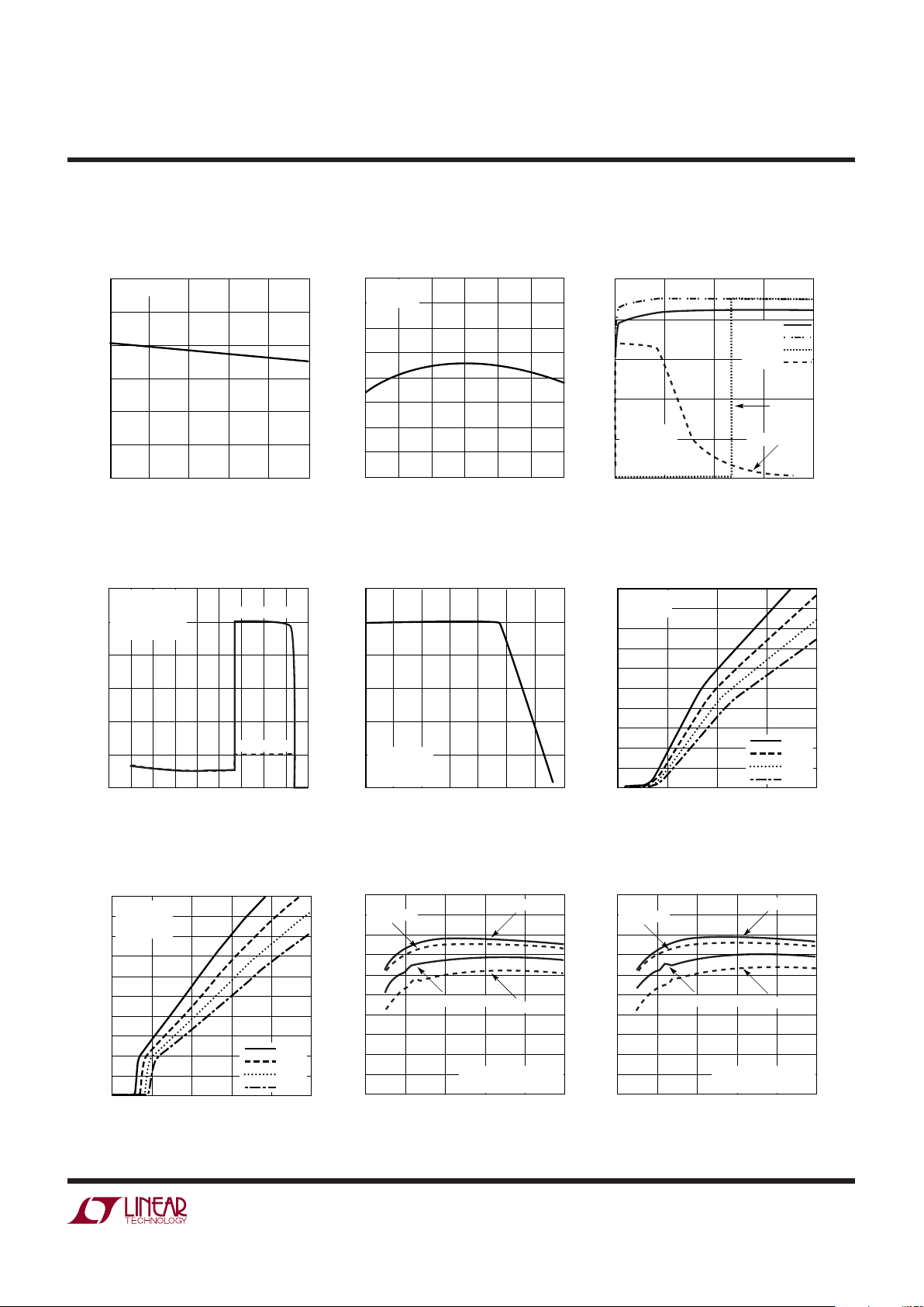
TYPICAL PERFORMANCE CHARACTERISTICS
V
FLOAT
Load Regulation
Battery Regulation (Float)
Voltage vs Temperature
Battery Current and Voltage vs
Time (LTC4089)
Charging from USB, I
BAT
vs V
BAT
Charge Current vs Temperature
(Thermal Regulation)
Ideal Diode Current vs Forward
Voltage and Temperature (No
External Device)
Ideal Diode Current vs Forward
Voltage and Temperature with
External Device
LTC4089 High Voltage Regulator
Effi ciency vs Output Load
LTC4089-5 High Voltage
Regulator Effi ciency vs Output
Load
T
A
= 25°C, unless otherwise specifi ed.
Page 6
LTC4089/LTC4089-5
6
40895fb
VIN (V)
5
1.6
1.5
1.4
1.3
1.2
1.1
1.0
0.9
20 30
40895 G10
10 15
25 35
I
OUT
(A)
MINIMUM
TYPICAL
VIN (V)
5
1.8
1.6
1.5
1.4
1.3
1.2
1.1
1.0
0.9
20 30
40895 G11
10 15
25 35
I
OUT
(A)
MINIMUM
TYPICAL
SWITCH CURRENT (A)
0
V
CE(SW)
(mV)
150
450
500
550
0.4
0.8
1.0
40895 G12
50
350
250
100
400
0
300
200
0.2
0.6
1.4
1.2
1.6
1.8
TA = 25°C
TA = 85°C
TA = –40°C
TEMPERATURE (°C)
FREQUENCY (kHz)
720
760
800
125
40895 G13
680
640
700
740
780
660
620
600
–25–50
250
75 100 150
50
FEEDBACK VOLTAGE (mV)
0
SWITCHING FREQUENCY (kHz)
400
600
800
40895 G14
200
0
200
400
600
100
300
500
700
800
300
500
100
700
SHDN PIN VOLTAGE (V)
0
0
SWITCH CURRENT LIMIT (A)
0.2
0.6
0.8
1.0
2.0
1.4
0.50 1 1.25
40895 G15
0.4
1.6
1.8
1.2
0.25 0.75 1.50 1.75 2
DUTY CYCLE (%)
0
CURRENT LIMIT (A)
1.6
1.8
2.0
80
40895 G16
1.4
1.2
1.5
1.7
1.9
1.3
1.1
1.0
2010
4030
60 70 90
50
100
TA = –40°C
T
A
= –5°C
T
A
= 25°C
T
A
= 90°C
LOAD CURRENT (mA)
1
5.8
INPUT VOLTAGE (V)
6.0
6.2
6.4
6.6
10 100 1000
40895 G17
5.6
5.4
5.2
5.0
6.8
7.0
TO START
TO RUN
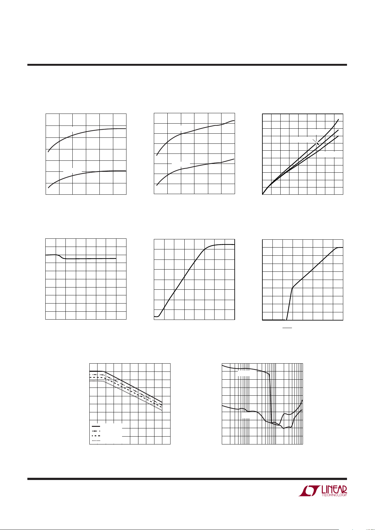
TYPICAL PERFORMANCE CHARACTERISTICS
High Voltage Regulator
Maximum Load Current, L = 10µH
High Voltage Regulator
Maximum Load Current, L = 33µH
High Voltage Regulator
Switch Voltage Drop
High Voltage Regulator
Switch Frequency
High Voltage Regulator
Frequency Foldback
High Voltage Regulator
Soft-Start
High Voltage Switch Current Limit
High Voltage Regulator
Typical Minimum Input Voltage
T
A
= 25°C, unless otherwise specifi ed.
Page 7
LTC4089/LTC4089-5
7
40895fb
1ms/DIV
V
IN
5V/DIV
V
OUT
5V/DIV
I
IN
0.5A/DIV
I
BAT
0.5A/DIV
40895 G18
V
BAT
= 3.85V
I
OUT
= 100mA
1ms/DIV
V
IN
5V/DIV
V
OUT
5V/DIV
I
IN
0.5A/DIV
I
BAT
0.5A/DIV
40895 G19
V
BAT
= 3.85V
I
OUT
= 100mA
100µs/DIV
HPWR
5V/DIV
I
IN
0.5A/DIV
I
BAT
0.5A/DIV
40895 G20
V
BAT
= 3.85V
I
OUT
= 50mA
1ms/DIV
WALL
5V/DIV
V
OUT
5V/DIV
I
WALL
0.5A/DIV
I
BAT
0.5A/DIV
40895 G21
V
BAT
= 3.85V
I
OUT
= 100mA
R
PROG
= 100k
1ms/DIV
WALL
5V/DIV
V
OUT
5V/DIV
I
WALL
0.5A/DIV
I
BAT
0.5A/DIV
40895 G22
V
BAT
= 3.85V
I
OUT
= 100mA
R
PROG
= 100k
100µs/DIV
SUSP
5V/DIV
V
OUT
5V/DIV
I
IN
0.5A/DIV
I
BAT
0.5A/DIV
40895 G23
V
BAT
= 3.85V
I
OUT
= 50mA
20µS/DIV
H
VOUT
50mV/DIV
I
OUT
0.5A/DIV
40895 G24
20µS/DIV
H
VOUT
50mV/DIV
I
L
0.5A/DIV
40895 G25
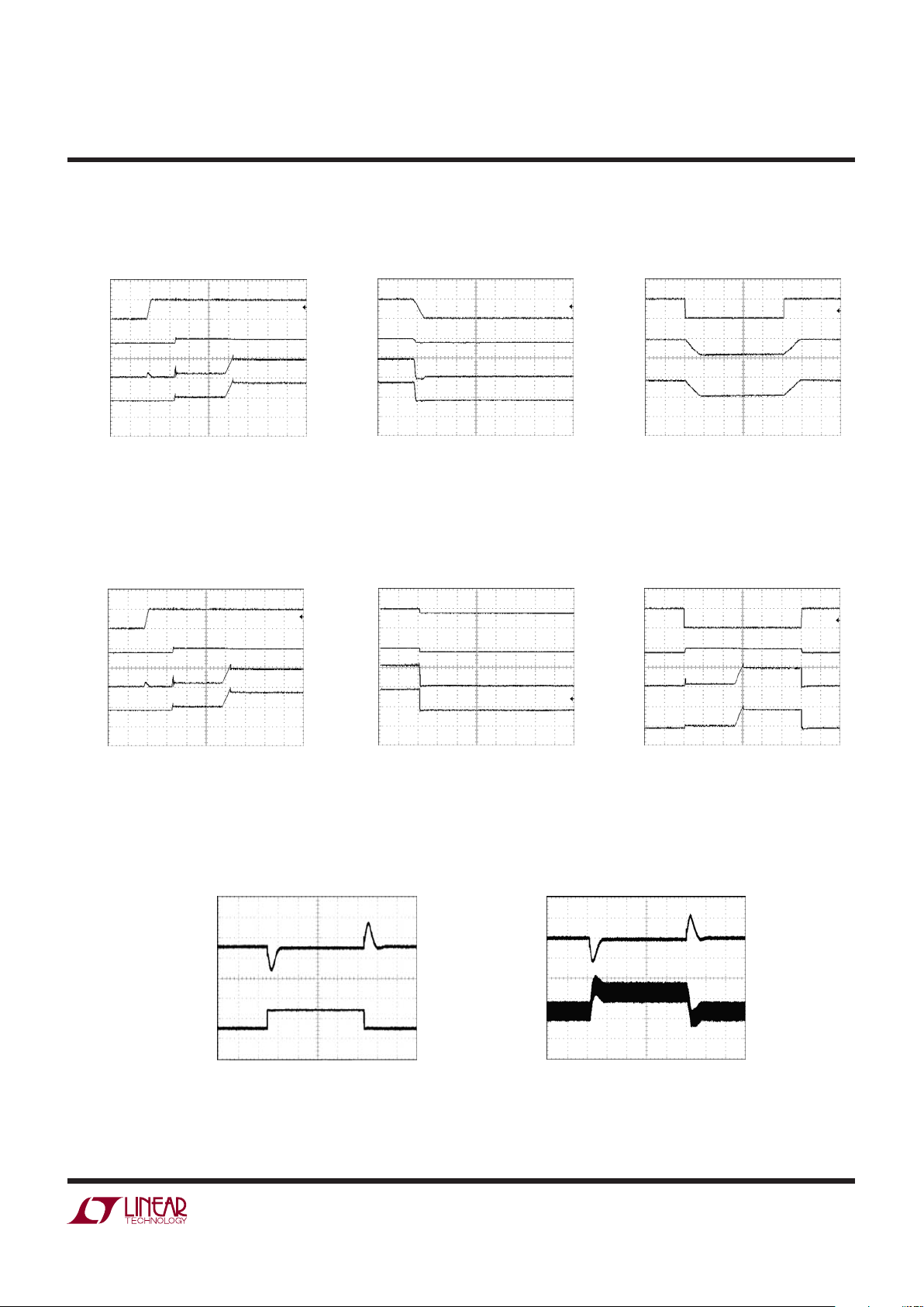
Input Connect Waveforms
TYPICAL PERFORMANCE CHARACTERISTICS
Input Disconnect Waveforms Response to HPWR
Wall Connect Waveforms
Wall Disconnect Waveforms Response to Suspend
High Voltage Regulator Load
Transient
High Voltage Regulator Load
Transient
T
A
= 25°C, unless otherwise specifi ed.
Page 8

LTC4089/LTC4089-5
8
40895fb
PI FU CTIO S
UUU
GND (Pins 1, 2): Ground. Tie the GND pin to a local ground
plane below the LTC4089 and the circuit components.
HVOUT (Pins 3, 18): Voltage Output of the High Voltage
Regulator. When suffi cient voltage is present at HVOUT,
the low voltage power path from IN to OUT will be disconnected and the HVPR pin will be pulled low to indicate
that a high voltage wall adapter has been detected. The
LTC4089 high voltage regulator will maintain just enough
differential voltage between HVOUT and BAT to keep the
battery charger MOSFET out of dropout (typically 300mV
from OUT to BAT). The LTC4089-5 high voltage regulator will provide a fi xed 5V output to the battery charger
MOSFET. HVOUT should be bypassed with at least 10µF
to GND. Connect pins 3 and 18 with a resistance no
greater than 1
.
V
C
(Pin 4): Leave the VC pin fl oating or bypass to ground
with a 10pF capacitor. This optional 10pF capacitor reduces
HVOUT ripple in discontinuous mode.
NTC (Pin 5): Input to the NTC Thermistor Monitoring
Circuits. Under normal operation, tie a thermistor from
the NTC pin to ground and a resistor of equal value from
NTC to VNTC. When the voltage on this pin is above 0.74
• V
VNTC
(Cold, 0°C) or below 0.29 • V
VNTC
(Hot, 50°C)
the timer is suspended but not cleared, the charging is
disabled and the CHRG pin remains in its former state.
When the voltage on NTC comes back between 0.74 •
V
VNTC
and 0.29 • V
VNTC
, the timer continues where it
left off and charging is re-enabled if the battery voltage
is below the recharge threshold. There is approximately
3°C of temperature hysteresis associated with each of the
input comparators.
Connect the NTC pin to ground to disable this feature. This
will disable all of the LTC4089 NTC functions.
VNTC (Pin 6): Output Bias Voltage for NTC. A resistor from
this pin to the NTC pin will bias the NTC thermistor.
HVPR (Pin 7): High Voltage Present Output. Active low
open drain output pin. A low on this pin indicates that the
high voltage regulator has suffi cient voltage to charge the
battery. This feature is disabled if no power is present on
HVIN, IN or BAT (i.e., below UVLO thresholds).
CHRG (Pin 8): Open-Drain Charge Status Output. When the
battery is being charged, the CHRG pin is pulled low by an
internal N-channel MOSFET. When the timer runs out or
the charge current drops below 10% of the programmed
charge current or the input supply is removed, the CHRG
pin is forced to a high impedance state.
PROG (Pin 9): Charge Current Program. Connecting a
resistor, R
PROG
, to ground programs the battery charge
current. The battery charge current is programmed
as follows:
IA
V
R
CHG
PROG
(),=
50 000
GATE (Pin 10): External ideal diode gate pin. This pin can
be used to drive the gate of an optional external PFET connected between BAT (drain) and OUT (source). By doing
so, the impedance of the ideal diode between BAT and
OUT can be reduced. When not in use, this pin should be
left fl oating. It is important to maintain a high impedance
on this pin and minimize all leakage paths.
BAT (Pin 11): Connect to a single cell Li-Ion battery. This
pin is used as an output when charging the battery and as
an input when supplying power to OUT. When the OUT pin
potential drops below the BAT pin potential, an ideal diode
function connects BAT to OUT and prevents V
OUT
from
dropping more than 100mV below V
BAT
. A precision internal
resistor divider sets the fi nal fl oat (charging) potential on
this pin. The internal resistor divider is disconnected when
IN and HVIN are in undervoltage lockout.
IN (Pin 12): Input Supply. Connect to USB supply, V
BUS
.
Input current to this pin is limited to either 20% or 100%
of the current programmed by the CLPROG pin as determined by the state of the HPWR pin. Charge current
(to the BAT pin) supplied through the input is set to the
current programmed by the PROG pin but will be limited
by the input current limit if charge current is set greater
than the input current limit.
Page 9

LTC4089/LTC4089-5
9
40895fb
PI FU CTIO S
UUU
OUT (Pin 13): Voltage Output. This pin is used to provide
controlled power to a USB device from either USB V
BUS
(IN), an external high voltage supply (HVIN), or the battery
(BAT) when no other supply is present. The high voltage
supply is prioritized over the USB V
BUS
input. OUT should
be bypassed with at least 4.7µF to GND.
CLPROG (Pin 14): Current Limit Program and Input Current Monitor. Connecting a resistor, R
CLPROG
, to ground
programs the input to output current limit. The current
limit is programmed as follows:
IA
V
R
CL
CLPROG
()=
1000
In USB applications, the resistor R
CLPROG
should be set
to no less than 2.1k. The voltage on the CLPROG pin is
always proportional to the current fl owing through the
IN to OUT power path. This current can be calculated
as follows:
IA
V
R
IN
CLPROG
CLPROG
() •= 1000
HPWR (Pin 15): High Power Select. This logic input is used
to control the input current limit. A voltage greater than
2.3V on the pin will set the input current limit to 100% of
the current programmed by the CLPROG pin. A voltage
less than 0.3V on the pin will set the input current limit to
20% of the current programmed by the CLPROG pin. A
2µA pull-down current is internally connected to this pin
to ensure it is low at power up when the pin is not being
driven externally.
SUSP (Pin 16): Suspend Mode Input. Pulling this pin
above 2.3V will disable the power path from IN to OUT.
The supply current from IN will be reduced to comply
with the USB specifi cation for suspend mode. Both the
ability to charge the battery from HVIN and the ideal diode
function (from BAT to OUT) will remain active. Suspend
mode will reset the charge timer if V
OUT
is less than V
BAT
while in suspend mode. If V
OUT
is kept greater than V
BAT
,
such as when the high voltage input is present, the charge
timer will not be reset when the part is put in suspend.
A 2µA pull-down current is internally applied to this pin
to ensure it is low at power-up when the pin is not being
driven externally.
TIMER (Pin 17): Timer Capacitor. Placing a capacitor,
C
TIMER
, to GND sets the timer period. The timer period is:
t hours
C R hours
µF k
TIMER
TIMER PROG
()
••
.•
=
3
0 1 100
Charge time is increased if charge current is reduced
due to undervoltage current limit, load current, thermal
regulation and current limit selection (HPWR).
Shorting the TIMER pin to GND disables the battery
charging functions.
SW (Pin 19): The SW pin is the output of the internal high
voltage power switch. Connect this pin to the inductor,
catch diode and boost capacitor.
BOOST (Pin 20): The BOOST pin is used to provide a
drive voltage, higher than the input voltage, to the internal
bipolar NPN power switch.
HVIN (Pin 21): The HVIN pin supplies current to the internal high voltage regulator and to the internal high voltage
power switch. The presence of a high voltage input takes
priority over the USB V
BUS
input (i.e., when a high voltage input supply is detected, the USB IN to OUT path is
disconnected). This pin must be locally bypassed.
HVEN (Pin 22): The HVEN pin is used to disable the high
voltage input path. Tie to ground to disable the high voltage
input or tie to at least 2.3V to enable the high voltage path.
If this feature is not used, tie to the HVIN pin. This pin can
also be used to soft-start the high voltage regulator; see
the Applications Information section.
EXPOSED PAD (Pin 23): Ground. The exposed package
pad is ground and must be soldered to the PC board for
proper functionality and for maximum heat transfer (use
several vias directly under the LTC4089).
Page 10

LTC4089/LTC4089-5
10
40895fb
BLOCK DIAGRA
W
–
+
SOFT-START
0.25V
SOFT-START2
–
+
–
+
–
+
–
+
15
TOO COLD
NTC
CURRENT LIMIT
TOO HOT
0.1V
NTC ENABLE
V
NTC
14
NTC
10k
100k
100k
–
+
13
HPWR
22
CLPROG
IN
23
PROG
CHG
1V
500mA/100mA
2µA
–
+
–
+
CURRENT CONTROL
OSCILLATOR
CHARGE CONTROL
CONTROL LOGIC
VOLTAGE DETECT
COUNTER
OSCILLATOR
TA
DIE
TEMP 105°C
I
LIM
2.8V
BATTERY
UVLO
4.1V
RECHARGE
UVLO
IN OUT BAT
I
CHG
BAT UV
RECHRG
HOLD
RESET
NTCERR
CLK
EOC
C/10
–
+
–
+
11
2µA
16
GND SUSP
2k
V
SET
IN
DRIVER
HVOUT
OUT
GATE
BATBAT
HVPR
21
TIMER
18
CHRG
STOP
4089 TA01
1V
CL
I
LIM
CNTL
ENABLE
–
+
EDA
19
D1
C3
L1
I
IN
1000
10
C4
R3
10pF
HVEN
HVIN
V
C
10
CC/CV REGULATOR
CHARGER
ENABLE
–
+
–
+
4.25V (RISING)
3.15V (FALLING)
–
+
21
21
21
1.8V
RSQ
10
C1
ENABLE
10
–
+
+
350mV
(LTC4089)
75mV (RISING)
25mV (FALLING)
GM
BOOST
Q1
D2
SW
25mV
25mV
IDEAL
DIODE
Q
DRIVER
+
–
+
–
+–+
–
PART NUMBER
LTC4089
LTC4089-5
V
SET
3.6V
5V
Page 11

LTC4089/LTC4089-5
11
40895fb
OPERATIO
U
The LTC4089/LTC4089-5 is a complete PowerPath™
controller for battery powered USB applications. The
LTC4089/LTC4089-5 is designed to receive power from a
low voltage source (e.g., USB or 5V wall adapter), a high
voltage source (e.g., FireWire/IEEE1394, automotive battery, 12V wall adapter, etc.), and a single-cell Li-Ion battery.
It can then deliver power to an application connected to the
OUT pin and a battery connected to the BAT pin (assuming
that an external supply other than the battery is present). Power supplies that have limited current resources
(such as USB V
BUS
supplies) should be connected to the
IN pin which has a programmable current limit. Battery
charge current will be adjusted to ensure that the sum of
the charge current and load current does not exceed the
programmed input current limit (see Figure 1).
An ideal diode function provides power from the battery
when output / load current exceeds the input current limit or
when input power is removed. Powering the load through
the ideal diode instead of connecting the load directly to
the battery allows a fully charged battery to remain fully
charged until external power is removed. Once external
power is removed the output drops until the ideal diode is
forward biased. The forward biased ideal diode will then
provide the output power to the load from the battery.
The LTC4089/LTC4089-5 also includes a high voltage
switching regulator which has the ability to receive power
from a high voltage input. This input takes priority over the
USB V
BUS
input (i.e., if both HVIN and IN are present, load
current and charge current will be delivered via the high
voltage path). When enabled, the high voltage regulator
regulates the HVOUT voltage using a 750kHz constant
frequency, current mode regulator. An external PFET between HVOUT (drain) and OUT (source) is turned on via
the HVPR pin allowing OUT to charge the battery and/or
supply power to the application. The LTC4089 maintains
approximately 300mV between the OUT pin and the BAT
pin, while the LTC4089-5 provides a fi xed 5V output.
Input Current Limit
Whenever the input power path is enabled (i.e., SUSP =
0V and HVIN = 0V) and power is available at IN, power
is delivered to OUT. The current limit and charger control
circuits of the LTC4089/LTC4089-5 are designed to limit
(Refer to Block Diagram)
HVOUT
OUT
GATE
BATBAT
OUT
HVPR
4089 F01
–
+
EDA
19
D1
L1
CC/CV REGULATOR
CHARGER
HIGH VOLTAGE
BUCK REGULATOR
USB CURRENT LIMIT
ENABLE
–
+
–
+
21
21
21
C1
HVIN
IN
Q1
SW
25mV
25mV
IDEAL
DIODE
4.25V (RISING)
3.15V (FALLING)
75mV (RISING)
25mV (FALLING)
+
LOAD
LI-ION
+
–
+
–
+
–
Figure 1. Simplifi ed PowerPath Block Diagram
PowerPath is a registered trademark of Linear Technology Corporation.
Page 12

LTC4089/LTC4089-5
12
40895fb
I
IN
I
LOAD(mA)
0
300
400
500
400 500300
4089 G01
200
100
100 200
0
CURRENT (mA)
I
LOAD
I
BAT
(CHARGING)
I
BAT
(IDEAL DIODE)
I
IN
I
LOAD(mA)
0
60
80
100
80 10060
4089 G02
40
20
20 40
0
CURRENT (mA)
I
LOAD
I
BAT
(CHARGING)
I
BAT
(IDEAL DIODE)
I
LOAD (mA)
0
300
400
500
400 500300
4089 G03
200
100
100 200
0
CURRENT (mA)
I
IN
I
LOAD
I
BAT
= I
CHG
I
BAT
= I
CL
= I
OUT
I
BAT
(CHARGING)
I
BAT
(IDEAL DIODE)
input current as well as control battery charge current
as a function of I
OUT
. The input current limit, ICL, can be
programmed using the following formula:
I
R
V
V
R
CL
CLPROG
CLPROG
CLPROG
=
⎡
⎣
⎢
⎤
⎦
⎥
=
1000 1000
•
where V
CLPROG
is the CLPROG pin voltage (typically 1V)
and R
CLPROG
is the total resistance from the CLPROG pin
to ground. For best stability over temperature and time,
1% metal fi lm resistors are recommended.
The programmed battery charge current, I
CHG
, is
defi ned as:
I
R
V
V
R
CHG
PROG
PROG
PROG
=
⎡
⎣
⎢
⎤
⎦
⎥
=
50 000 50 000,
•
,
Input current, IIN, is equal to the sum of the BAT pin
output current and the OUT pin output current. V
CLPROG
will typically servo to 1V, however, if I
OUT
+ I
BAT
< ICL
then V
CLPROG
will track the input current according to the
following equation:
II I
V
R
IN OUT BAT
CLPROG
CLPROG
=+= • 1000
The current limiting circuitry in the LTC4089/LTC4089-5
can and should be confi gured to limit current to 500mA
for USB applications (selectable using the HPWR pin and
programmed using the CLPROG pin).
OPERATIO
U
Figure 2. Input and Battery Currents as a Function of Load Current
The LTC4089/LTC4089-5 reduces battery charge current
such that the sum of the battery charge current and the
load current does not exceed the programmed input current
limit (one-fi fth of the programmed input current limit when
HPWR is low, see Figure 2). The battery charge current
goes to zero when load current exceeds the programmed
input current limit (one-fi fth of the limit when HPWR is
low). Even if the battery charge current is set to exceed
the allowable USB current, the USB specifi cation will not
be violated. The battery charger will reduce its current as
needed to ensure that the USB specifi cation is not exceeded.
If the load current is greater than the current limit, the
output voltage will drop to just under the battery voltage
where the ideal diode circuit will take over and the excess
load current will be drawn from the battery.
In USB applications, the minimum value for R
CLPROG
should be 2.1k. This will prevent the input current from
exceeding 500mA due to LTC4089/LTC4089-5 tolerances
and quiescent currents. A 2.1k CLPROG resistor will give a
typical current limit of 476mA in high power mode (HPWR
= 1) or 95mA in low power mode (HPWR = 0).
When SUSP is driven to a logic high, the input power
path is disabled and the ideal diode from BAT to OUT will
supply power to the application.
(a) High Power Mode/Full Charge
R
PROG
= 100k and R
CLPROG
= 2k
(b) Low Power Mode/Full Charge
R
PROG
= 100k and R
CLPROG
= 2k
(c) High Power Mode with
I
CL
= 500mA and I
CHG
= 250mA
R
PROG
= 200k and R
CLPROG
= 2k
Page 13

LTC4089/LTC4089-5
13
40895fb
High Voltage Step Down Regulator
The power delivered from HVIN to HVOUT is controlled
by a 750kHz constant frequency, current mode step down
regulator. An external P-channel MOSFET directs this
power to OUT and prevents reverse conduction from OUT
to HVOUT (and ultimately HVIN).
A 750kHz oscillator enables an RS fl ip-fl op, turning on the
internal 1.95A power switch Q1. An amplifi er and comparator monitor the current fl owing between the HVIN and SW
pins, turning the switch off when this current reaches a
level determined by the voltage at V
C
. An error amplifi er
servos the V
C
node to maintain approximately 300mV
between OUT and BAT (LTC4089). By keeping the voltage
across the battery charger low, effi ciency is optimized
because power lost to the battery charger is minimized
and power available to the external load is maximized. If
the BAT pin voltage is less than approximately 3.3V, then
the error amplifi er will servo the V
C
node to provide a
constant HVOUT output voltage of about 3.6V. An active
clamp on the V
C
node provides current limit. The VC node
is also clamped to the voltage on the HVEN pin; soft-start
is implemented by a voltage ramp at the HVEN pin using
an external resistor and capacitor.
An internal regulator provides power to the control circuitry.
This regulator includes an undervoltage lockout to prevent
switching when HVIN is less than about 4.7V. The HVEN
pin is used to disable the high voltage regulator. HVIN
input current is reduced to less than 2µA and the external
P-channel MOSFET disconnects HVOUT from OUT when
the high voltage regulator is disabled.
The switch driver operates from either the high voltage
input or from the BOOST pin. An external capacitor and
diode are used to generate a voltage at the BOOST pin that
is higher than the input supply. This allows the driver to
fully saturate the internal bipolar NPN power switch for
effi cient operation.
When HVOUT is below 3.95V the operating frequency
is reduced. This frequency foldback helps to control the
regulator output current during start-up and overload.
Ideal Diode from BAT to OUT
The LTC4089/LTC4089-5 has an internal ideal diode as
well as a controller for an optional external ideal diode. If
a battery is the only power supply available, or if the load
current exceeds the programmed input current limit, then
the battery will automatically deliver power to the load via
an ideal diode circuit between the BAT and OUT pins. The
ideal diode circuit (along with the recommended 4.7µF
capacitor on the OUT pin) allows the LTC4089/LTC4089-5
to handle large transient loads and wall adapter or USB
V
BUS
connect/disconnect scenarios without the need for
large bulk capacitors. The ideal diode responds within
a few microseconds and prevents the OUT pin voltage
from dropping signifi cantly below the BAT pin voltage.
A comparison of the I-V curve of the ideal diode and a
Schottky diode can be seen in Figure 3.
If the input current increases beyond the programmed
input current limit additional current will be drawn from the
battery via the internal ideal diode. Furthermore, if power
to IN (USB V
BUS
) or HVIN (high voltage input) is removed,
then all of the application power will be provided by the
battery via the ideal diode. A 4.7µF capacitor at OUT is
suffi cient to keep a transition from input power to battery
power from causing signifi cant output voltage droop. The
ideal diode consists of a precision amplifi er that enables a
large P-channel MOSFET transistor whenever the voltage
at OUT is approximately 20mV (V
FWD
) below the voltage
at BAT. The resistance of the internal ideal diode is approximately 200m
. If this is suffi cient for the application
OPERATIO
U
Figure 3. LTC4089/LTC4089-5 Versus
Schottky Diode Forward Voltage Drop
CONSTANT
I
0N
CONSTANT
R
0N
CONSTANT
V
0N
V
FWD
I
MAX
FORWARD VOLTAGE (V)
4089 F03
I
FWD
0
CURRENT (A)
SLOPE: 1/R
DIO(ON)
SLOPE: 1/R
FWD
SCHOTTKY
DIODE
LTC4089
Page 14

LTC4089/LTC4089-5
14
40895fb
then no external components are necessary. However,
if more conductance is needed, an external P-channel
MOSFET can be added from BAT to OUT. The GATE pin
of the LTC4089/LTC4089-5 drives the gate of the PFET for
automatic ideal diode control. The source of the external
MOSFET should be connected to OUT and the drain should
be connected to BAT. In order to help protect the external
MOSFET in over-current situations, it should be placed in
close thermal contact to the LTC4089/LTC4089-5.
Battery Charger
The battery charger circuits of the LTC4089/LTC4089-5
are designed for charging single cell lithium-ion batteries. Featuring an internal P-channel power MOSFET, the
charger uses a constant-current/constant-voltage charge
algorithm with programmable current and a programmable timer for charge termination. Charge current can be
programmed up to 1.2A. The fi nal fl oat voltage accuracy
is ±0.8% typical. No blocking diode or sense resistor is
required when powering either the IN or the HVIN pins.
The CHRG open-drain status output provides information
regarding the charging status of the LTC4089/LTC4089-5
at all times. An NTC input provides the option of charge
qualifi cation using battery temperature.
An internal thermal limit reduces the programmed charge
current if the die temperature attempts to rise above a
preset value of approximately 105°C. This feature protects
the LTC4089/LTC4089-5 from excessive temperature, and
allows the user to push the limits of the power handling
capability of a given circuit board without risk of damaging the LTC4089/LTC4089-5. Another benefi t of the
LTC4089/LTC4089-5 thermal limit is that charge current
can be set according to typical, not worst-case, ambient
temperatures for a given application with the assurance
that the charger will automatically reduce the current in
worst-case conditions.
The charge cycle begins when the voltage at the OUT
pin rises above the battery voltage and the battery voltage is below the recharge threshold. No charge current
actually fl ows until the OUT voltage is 100mV above
the BAT voltage. At the beginning of the charge cycle, if
the battery voltage is below 2.8V, the charger goes into
trickle charge mode to bring the cell voltage up to a safe
level for charging. The charger goes into the fast charge
constant-current mode once the voltage on the BAT pin
rises above 2.8V. In constant current mode, the charge
current is set by R
PROG
. When the battery approaches the
fi nal fl oat voltage, the charge current begins to decrease
as the LTC4089/LTC4089-5 switches to constant-voltage
mode. When the charge current drops below 10% of the
programmed charge current while in constant-voltage
mode the CHRG pin assumes a high impedance state.
An external capacitor on the TIMER pin sets the total
minimum charge time. When this time elapses the
charge cycle terminates and the CHRG pin assumes a
high impedance state, if it has not already done so. While
charging in constant current mode, if the charge current
is decreased by thermal regulation or in order to maintain
the programmed input current limit the charge time is
automatically increased. In other words, the charge time is
extended inversely proportional to the actual charge current
delivered to the battery. For Li-Ion and similar batteries that
require accurate fi nal fl oat potential, the internal bandgap
reference, voltage amplifi er and the resistor divider provide
regulation with ±0.8% accuracy.
Trickle Charge and Defective Battery Detection
At the beginning of a charge cycle, if the battery voltage is low (below 2.8V) the charger goes into trickle
charge reducing the charge current to 10% of the fullscale current. If the low battery voltage persists for one
quarter of the total charge time, the battery is assumed
to be defective, the charge cycle is terminated and the
CHRG pin output assumes a high impedance state. If
for any reason the battery voltage rises above ~2.8V the
charge cycle will be restarted. To restart the charge cycle
(i.e., when the dead battery is replaced with a discharged
battery), simply remove the input voltage and reapply it
or cycle the TIMER pin to 0V.
Programming Charge Current
The formula for the battery charge current is:
II
V
R
CHG PROG
PROG
PROG
==•, •,50 000 50 000
where V
PROG
is the PROG pin voltage and R
PROG
is the total
resistance from the PROG pin to ground. Keep in mind that
OPERATIO
U
Page 15

LTC4089/LTC4089-5
15
40895fb
when the LTC4089/LTC4089-5 is powered from the IN pin,
the programmed input current limit takes precedent over
the charge current. In such a scenario, the charge current
cannot exceed the programmed input current limit.
For example, if typical 500mA charge current is required,
calculate:
R
V
mA
k
PROG
==
1
500
50 000 100•,
For best stability over temperature and time, 1% metal fi lm
resistors are recommended. Under trickle charge conditions,
this current is reduced to 10% of the full-scale value.
The Charge Timer
The programmable charge timer is used to terminate the
charge cycle. The timer duration is programmed by an
external capacitor at the TIMER pin. The charge time is
typically:
t hours
C R hours
µF k
TIMER
TIMER PROG
()
••
.•
=
3
0 1 100
The timer starts when an input voltage greater than the
undervoltage lockout threshold level is applied or when
leaving shutdown and the voltage on the battery is less than
the recharge threshold. At power-up or exiting shutdown
with the battery voltage less than the recharge threshold
the charge time is a full cycle. If the battery is greater than
the recharge threshold the timer will not start and charging
is prevented. If after power-up the battery voltage drops
below the recharge threshold, or if after a charge cycle
the battery voltage is still below the recharge threshold,
the charge time is set to one-half of a full cycle.
The LTC4089/LTC4089-5 has a feature that extends charge
time automatically. Charge time is extended if the charge
current in constant current mode is reduced due to load
current or thermal regulation. This change in charge time
is inversely proportional to the change in charge current.
As the LTC4089/LTC4089-5 approaches constant voltage
mode the charge current begins to drop. This change in
charge current is due to normal charging operation and
does not affect the timer duration.
Consider, for example, a USB charge condition where
R
CLPROG
= 2k, R
PROG
= 100k and C
TIMER
= 0.1µF. This
corresponds to a three hour charge cycle. However, if the
HPWR input is set to a logic low, then the input current
limit will be reduced from 500mA to 100mA. With no additional system load, this means the charge current will
be reduced to 100mA. Therefore, the termination timer
will automatically slow down by a factor of fi ve until the
charger reaches constant voltage mode (i.e. V
BAT
= 4.2V)
or HPWR is returned to a logic high. The charge cycle is
automatically lengthened to account for the reduced charge
current. The exact time of the charge cycle will depend on
how long the charger remains in constant-current mode
and/or how long the HPWR pin remains a logic low.
Once a time-out occurs and the voltage on the battery is
greater than the recharge threshold, the charge current
stops, and the CHRG output assumes a high impedance
state if it has not already done so.
Connecting the TIMER pin to ground disables the battery
charger.
CHRG Status Output Pin
When the charge cycle starts, the CHRG pin is pulled to
ground by an internal N-channel MOSFET capable of driving an LED. When the charge current drops below 10%
of the programmed full charge current while in constant
voltage mode, the pin assumes a high impedance state,
but charge current continues to fl ow until the charge
time elapses. If this state is not reached before the end
of the programmable charge time, the pin will assume a
high impedance state when a time-out occurs. The CHRG
current detection threshold can be calculated by the following equation:
I
V
R
V
R
DETECT
PROG PROG
==
01
50 000
5000.
•,
For example, if the full charge current is programmed
to 500mA with a 100k PROG resistor the CHRG pin will
change state at a battery charge current of 50mA.
Note: The end-of-charge (EOC) comparator that monitors the charge current latches its decision. Therefore,
the fi rst time the charge current drops below 10% of the
programmed full charge current while in constant voltage mode, it will toggle CHRG to a high impedance state.
OPERATIO
U
Page 16

LTC4089/LTC4089-5
16
40895fb
If, for some reason the charge current rises back above
the threshold, the CHRG pin will not resume the strong
pull-down state. The EOC latch can be reset by a recharge
cycle (i.e., V
BAT
drops below the recharge threshold) or
toggling the input power to the part.
NTC Thermistor—Battery Temperature Charge
Qualifi cation
The battery temperature is measured by placing a negative temperature coeffi cient (NTC) thermistor close to the
battery pack. The NTC circuitry is shown in Figure 4.
To use this feature, connect the NTC thermistor (R
NTC
)
between the NTC pin and ground and a resistor (R
NOM
) from
the NTC pin to VNTC. R
NOM
should be a 1% resistor with
a value equal to the value of the chosen NTC thermistor at
25°C (this value is 10k for a Vishay NTHS0603N02N1002J
thermistor). The LTC4089/LTC4089-5 goes into hold mode
when the resistance (R
HOT
) of the NTC thermistor drops
to 0.41 times the value of R
NOM
, or approximately 4.1k,
which should be at 50°C. The hold mode freezes the timer
and stops the charge cycle until the thermistor indicates a
return to a valid temperature. As the temperature drops,
the resistance of the NTC thermistor rises. The LTC4089/
LTC4089-5 is designed to go into hold mode when the
value of the NTC thermistor increases to 2.82 times the
value of R
NOM
. This resistance is R
COLD
. For a Vishay
NTHS0603N02N1002J thermistor, this value is 28.2k
which corresponds to approximately 0°C. The hot and cold
comparators each have approximately 3°C of hysteresis
to prevent oscillation about the trip point. Grounding the
NTC pin will disable the NTC function.
Current Limit Undervoltage Lockout
An internal undervoltage lockout circuit monitors the
input voltage and disables the input current limit circuits
until V
IN
rises above the undervoltage lockout threshold.
The current limit UVLO circuit has a built-in hysteresis of
125mV. Furthermore, to protect against reverse current in
the power MOSFET, the current limit UVLO circuit disables
the current limit (i.e., forces the input power path to a high
impedance state) if V
OUT
exceeds VIN. If the current limit
UVLO comparator is tripped, the current limit circuits will
not come out of shutdown until V
OUT
falls 50mV below
the V
IN
voltage.
Charger Undervoltage Lockout
An internal undervoltage lockout circuit monitors the V
OUT
voltage and disables the battery charger circuits until
V
OUT
rises above the undervoltage lockout threshold. The
battery charger UVLO circuit has a built-in hysteresis of
125mV. Furthermore, to protect against reverse current
in the power MOSFET, the charger UVLO circuit keeps the
charger shut down if V
BAT
exceeds V
OUT
. If the charger
UVLO comparator is tripped, the charger circuits will
not come out of shutdown until V
OUT
exceeds V
BAT
by 50mV.
Suspend
The LTC4089/LTC4089-5 can be put in suspend mode by
forcing the SUSP pin greater than 2.3V. In suspend mode,
the ideal diode function from BAT to OUT is kept alive. If
power is applied to the HVIN pin, then charging will be
unaffected. Current drawn from the IN pin is reduced to
50µA. Suspend mode is intended to comply with the USB
power specifi cation mode of the same name.
OPERATIO
U
Figure 4. NTC Circuit
–
+
–
+
R
NOM
10k
R
NTC
10k
NTC
VNTC
6
0.1V
NTC_ENABLE
4089 F04
LTC4089
TOO_COLD
TOO_HOT
0.74 •
VNTC
0.29 • VNTC
–
+
5
Page 17

LTC4089/LTC4089-5
17
40895fb
USB and 5V Wall Adapter Power
Although the LTC4089/LTC4089-5 is designed to draw
power from a USB port, a higher power 5V wall adapter
can also be used to power the application and charge the
battery (higher voltage wall adapters can be connected
directly to HVIN). Figure 5 shows an example of combining
a 5V wall adapter and a USB power input. With its gate
grounded by 1k, P-channel MOSFET MP1 provides USB
power to the LTC4089/LTC4089-5 when 5V wall power is
not available. When 5V wall power is available, D1 both
supplies power to the LTC4089, pulls the gate of MN1 high
to increase the charge current (by increasing the input
current limit), and pulls the gate of MP1 high to disable it
and prevent conduction back to the USB port.
2k1k
MN1
2.87k
59k
IN
PROG
CLPROG
LTC4089
BAT
+
MP1
D1
I
CHG
Li-Ion
BATTERY
5V WALL
ADAPTER
850mA I
CHG
USB POWER
500mA I
CHG
4089 F05
Inductor Selection and Maximum Output Current
A good choice for the inductor value is L = 10µH. With this
value the maximum load current will be 1A. The RMS current
rating of the inductor must be greater than the maximum
load current and its saturation current should be about
30% higher. Note that the maximum load current
will be the programmed charge current plus the largest
expected application load current. For robust operation in
fault conditions, the saturation current should be ~2.3A. To
keep effi ciency high, the series resistance (DCR) should
be less than 0.1 . Table 1 lists several vendors and types
that are suitable.
Table 1: Inductor Vendors
VENDOR URL
PART
SERIES
INDUCTANCE
(µH)
SIZE
(mm)
Sumida www.sumida.com CDRH5D28 8.2, 10 6 6 3
CDRH6D38 10 7 7 4
TDK www.tdk.com SLF6028T 10 6 6 2.8
Toko www.toko.com D63LCB 10 6.3 6.3 3
Catch Diode
Depending on load current, a 1A to 2A Schottky diode is
recommended for the D1 catch diode. The diode must
have a reverse voltage rating equal to, or greater than,
the maximum input voltage. The ON Semiconductor
MBRM140 and the Diodes Inc. DFLS140/160/240 are
good choices.
High Voltage Regulator Capacitor Selection
Bypass the HVIN pin of the LTC4089/LTC4089-5 circuit
with a 1µF, or higher value ceramic capacitor of X7R or
X5R type. Y5V types have poor performance over temperature and applied voltage and should not be used. A 1µF
ceramic is adequate to bypass the high voltage input and
will easily handle the ripple current. However, if the input
power source has high impedance, or there is signifi cant
inductance due to long wires or cables, additional bulk
capacitance may be necessary. This can be provided with
a low performance electrolytic capacitor.
APPLICATIO S I FOR ATIO
WUU
U
Figure 5. USB or 5V Wall Adapter Power
Page 18

LTC4089/LTC4089-5
18
40895fb
The high voltage regulator output capacitor controls output
ripple, supplies transient load currents, and stabilizes the
regulator control loop. Ceramic capacitors have very low
equivalent series resistance (ESR) and provide the best
ripple performance. A good value is 10µF. Use X5R or
X7R types, and note that a ceramic capacitor biased with
V
HVOUT
will have less than its nominal capacitance. Table
2 lists several capacitor vendors.
Table 2: Capacitor Vendors
VENDOR PHONE URL
PART
SERIES
COM-
MENTS
Panasonic
(714) 373-7366
www.panasonic.com Ceramic,
Polymer,
Tantalum
EEF Series
Kemet
(864) 963-6300
www.kemet.com Ceramic,
Tantalum
T494,
T495
Sanyo
(408) 749-9714
www.sanyovideo.com Ceramic,
Polymer,
Tantalum
POSCAP
Murata
(404) 436-1300
www.murata.com Ceramic
AVX www.avxcorp.com Ceramic,
Tantalum
TPS
Series
Taiyo
Yuden
(864) 963-6300
www.taiyo-yuden.com Ceramic
BOOST Pin Considerations
Capacitor C3 and diode D2 (see Block Diagram) are used
to generate a boost voltage that is higher than the input
voltage. In most cases, a 0.1µF capacitor and fast-switching diode (such as the 1N4148 or 1N914) will work well.
The BOOST pin must be at least 2.2V above the SW pin
for proper operation.
High Voltage Regulator Soft-Start
The HVEN pin can be used to soft-start the high voltage
regulator and reduce the maximum input current during
start-up. A voltage ramp at the HVEN pin can be created
by driving the pin through an external RC fi lter (see Figure
6). By choosing a large RC time constant, the peak start-up
current will not overshoot the current that is required to
regulate the output. Choose the value of the resistor so that
it can supply 20µA when the HVEN pin reaches 2.3V.
RUN
15k
0.1µF
HVEN
GND
4089 F06
LTC4089
Alternate NTC Thermistors
The LTC4089/LTC4089-5 NTC trip points were designed
to work with thermistors whose resistance-temperature
characteristics follow Vishay Dale’s “R-T Curve 2.” The
Vishay NTHS0603N02N1002J is an example of such a
thermistor. However, Vishay Dale has many thermistor
products that follow the “R-T Curve 2” characteristic in a
variety of sizes. Furthermore, any thermistor whose ratio
of R
COLD
to R
HOT
is about 7.0 will also work (Vishay Dale
R-T Curve 2 shows a ratio of 2.815/0.4086 = 6.89).
Power conscious designs may want to use thermistors
whose room temperature value is greater than 10k. Vishay
Dale has a number of values of thermistor from 10k to 100k
that follow the “R-T Curve 2.” Using these as indicated
in the NTC Thermistor section will give temperature trip
points of approximately 3°C and 47°C, a delta of 44°C.
This delta in temperature can be moved in either direction by changing the value of R
NOM
with respect to R
NTC
.
APPLICATIO S I FOR ATIO
WUU
U
Figure 6. Using the HVEN Pin to Soft-Start the
High Voltage Regulator.
Page 19

LTC4089/LTC4089-5
19
40895fb
Increasing R
NOM
will move both trip points to lower
temperatures. Likewise, a decrease in R
NOM
with respect
to R
NTC
will move the trip points to higher temperatures.
To calculate R
NOM
for a shift to lower temperature, for
example, use the following equation:
R
R
RatC
NOM
COLD
NTC
=°
2 815
25
.
•
where R
COLD
is the resistance ratio of R
NTC
at the desired
cold temperature trip point. To shift the trip points to higher
temperatures use the following equation:
R
R
RatC
NOM
HOT
NTC
=°
0 4086
25
.
•
where R
HOT
is the resistance ratio of R
NTC
at the desired
hot temperature trip point.
The following example uses a 100K R-T Curve 1 Thermistor
from Vishay Dale. The difference between the trip points is
44°C, from before—and the desired cold trip point of 0°C,
would put the hot trip point at 44°C. The R
NOM
needed is
calculated as follows:
R
R
RatC
NOM
COLD
NTC
=°=
2 815
25
3 266
2 815
100
.
•
.
.
•kkkΩΩ= 116
The nearest 1% value for R
NOM
is 115k. This is the value
used to bias the NTC thermistor to get cold and hot trip
points of approximately 0°C and 44°C, respectively. To
extend the delta between the cold and hot trip points, a
resistor (R1) can be added in series with R
NTC
(see Figure
7). The values of the resistors are calculated as follows:
R
RR
R
NOM
COLD HOT
=
−
−
=
−
2 815 0 4086
1
0 4086
2 815 0
..
.
.
..•4086
⎡
⎣
⎢
⎤
⎦
⎥
−
[]
−RRR
COLD HOT HOT
where R
NOM
is the value of the bias resistor, R
HOT
and
R
COLD
are the values of R
NTC
at the desired temperature
trip points. Continuing the forementioned example with
a desired hot trip point of 50°C:
R
RR
k
NOM
COLD HOT
=
−
−
=
−
2 815 0 4086
100 3 266 0 3
..
•( . .
6602
2 815 0 4086
120 8 121 1
110
)
..
., %
−
=
=
k k nearest
R
00
0 4086
2 815 0 4086
3 266 0 3602
k•
.
..
•
..
−
⎛
⎝
⎜
⎞
⎠
⎟
−
()
−−
⎡
⎣
⎢
⎢
⎢
⎤
⎦
⎥
⎥
⎥
=
0 3602
13 3 13 3 1
.
., . %k k is nearest
The fi nal solution is shown in Figure 7, where
R
NOM
= 121k, R1 = 13.3k and R
NTC
= 100k at 25°C
–
+
–
+
R
NOM
121k
R
NTC
100k
R1
13.3k
NTC
VNTC
15
0.1V
NTC_ENABLE
4089 F07
TOO_COLD
TOO_HOT
0.74 •
VNTC
0.29 • VNTC
–
+
14
LTC4089
APPLICATIO S I FOR ATIO
WUU
U
Figure 7. Modifi ed NTC Circuit
Page 20

LTC4089/LTC4089-5
20
40895fb
Power Dissipation and High Temperature
Considerations
The die temperature of the LTC4089/LTC4089-5 must
be lower than the maximum rating of 110°C. This is
generally not a concern unless the ambient temperature
is above 85°C. The total power dissipated inside the
LTC4089/LTC4089-5 depends on many factors, including
input voltage (IN or HVIN), battery voltage, programmed
charge current, programmed input current limit, and load
current.
In general, if the LTC4089/LTC4089-5 is being powered
from IN the power dissipation can be calculated as follows:
PVV I VV I
D IN BAT BAT IN OUT OUT
=− +−()•()•
where PD is the power dissipated, I
BAT
is the battery
charge current, and I
OUT
is the application load current.
For a typical application, an example of this calculation
would be:
PVVAV VA
mW
D
=− +− =(.)•.(.)•.53704 547501
545
This example assumes VIN = 5V, V
OUT
= 4.75V, V
BAT
=
3.7V, I
BAT
= 400mA, and I
OUT
= 100mA resulting in slightly
more than 0.5W total dissipation.
If the LTC4089 is being powered from HVIN, the power
dissipation can be estimated by calculating the regulator
power loss from an effi ciency measurement, and subtracting the catch diode loss.
PVIIV
V
V
D HVOUT BAT OUT D
HVOUT
H
=− + −
−
( )•( •( )) •11η
VVIN
BAT OUT BAT
II VI
⎛
⎝
⎜
⎞
⎠
⎟
++•( ) . •03
where is the effi ciency of the high voltage regulator and
V
D
is the forward voltage of the catch diode at I = I
BAT
+ I
OUT
. The fi rst term corresponds to the power lost in
converting V
HVIN
to V
HVOUT
, the second term subtracts
the catch diode loss, and the third term is the power dis-
sipated in the battery charger. For a typical application,
an example of this calculation would be:
PVAAV
V
V
D
=− +
[]
−
−
⎛
⎝
( . )• •( . . ) . •1087 4 07 03 04
1
4
12
⎜⎜
⎞
⎠
⎟
++ =•( . . ) . • .07 03 03 07 463AA VA mW
This example assumes 87% effi ciency, V
HVIN
= 12V, V
BAT
= 3.7V (V
HVOUT
is about 4V), I
BAT
= 700mA, I
OUT
= 300mA
resulting in less than 0.5W total dissipation.
If the LTC4089-5 is being powered from HVIN, the power
dissipation can be estimated by calculating the regulator
power loss from an effi ciency measurement and subtracting the catch diode loss.
PVII
V
V
V
D BAT OUT
D
HVIN
=− +
−−
⎛
⎝
⎜
⎞
⎠
( )•( •( ))
•
15
1
5
η
⎟⎟
+
+−
•( )
()•
II
VV I
BAT OUT
BAT BAT
5
The difference between this equation and the LTC4089 is
the last term which represents the power dissipation in
the battery charger. For a typical application, an example
of this calculation would be:
PVAA
V
V
V
D
=− +
−−
(.)•(•(. .))
.•( )
1 0 87 5 0 7 0 3
04 1
5
12
••( . . )
(.)•.,
07 03
537071327
AA
VVA mW
+
+− =
Like the LTC4089 example, this example assumes 87%
effi ciency, V
HVIN
= 12V, V
BAT
= 3.7V, I
BAT
= 700mA, I
OUT
= 300mA resulting in 1.3W total dissipation.
To prevent power dissipation of this magnitude from
causing high die temperature, it is important to solder the
exposed backside of the package to a ground plane. This
ground should be tied to other copper layers below with
thermal vias; these layers will spread the heat dissipated
by the LTC4089. Additional vias should be placed near the
catch diodes. Adding more copper to the top and bottom
layers, and tying this copper to the internal planes with
vias, can reduce thermal resistance further. With these
steps, the thermal resistance from die (i.e., junction) to
ambient can be reduced to
JA
= 40°C/W.
APPLICATIO S I FOR ATIO
WUU
U
Page 21

LTC4089/LTC4089-5
21
40895fb
APPLICATIO S I FOR ATIO
WUU
U
The power dissipation in the other power components—catch diodes, MOSFETs, boost diodes and inductors—causes additional copper heating and can further
increase the “ambient” temperature of the IC.
Board Layout Considerations
As discussed in the previous section, it is critical that
the exposed metal pad on the backside of the LTC4089/
LTC4089-5 package be soldered to the PC board ground.
Furthermore, proper operation and minimum EMI requires
a careful printed circuit board (PCB) layout. Note that large,
switched currents fl ow in the power switch (between the
HVIN and SW pins), the catch diode and the HVIN input
capacitor. These components, along with the inductor and
output capacitor, should be placed on the same side of
the circuit board, and their connections should be made
on that layer. Place a local, unbroken ground plane below
these components. The loop formed by these components
should be as small as possible. Additionally, the SW and
BOOST nodes should be kept as small as possible. Figure
8 shows the recommended component placement with
trace and via locations.
High frequency currents, such as the high voltage input
current of the LTC4089, tend to fi nd their way along
the ground plane on a mirror path directly beneath the
incident path on the top of the board. If there are slits or
cuts in the ground plane due to other traces on that layer,
the current will be forced to go around the slits. If high
frequency currents are not allowed to fl ow back through
their natural least-area path, excessive voltage will build
up and radiated emissions will occur. See Figure 9.
4089 F09
VIN and V
HVIN
Bypass Capacitor
Many types of capacitors can be used for input bypassing,
however, caution must be exercised when using multilayer
ceramic capacitors. Because of the self-resonant and high
Q characteristics of some types of ceramic capacitors,
high voltage transients can be generated under some
start-up conditions, such as from connecting the charger
input to a hot power source. For more information, refer
to Application Note 88.
Battery Charger Stability Considerations
The constant-voltage mode feedback loop is stable without
any compensation when a battery is connected with low
impedance leads. Excessive lead length, however, may add
enough series inductance to require a bypass capacitor
of at least 1µF from BAT to GND. Furthermore, a 4.7µF
capacitor with a 0.2 to 1 series resistor to GND is
recommended at the BAT pin to keep ripple voltage low
when the battery is disconnected.
Figure 8. Suggested Board Layout
Figure 9. Ground Currents Follow Their Incident Path
at High Speed. Slices in the Ground Plane Cause High
Voltage and Increased Emissions.
MINIMIZE D1, L1,
C3, U1, SW PIN LOOP
MINIMIZE TRACE LENGTH
U1 THERMAL PAD
SOLDERED TO PCB.
VIAS CONNECTED TO ALL
GND PLANES WITHOUT
THERMAL RELIEF.
C1 AND D1
GND PADS
SIDE-BY-SIDE
AND SEPERATED
WITH C3 GND PAD
Page 22

LTC4089/LTC4089-5
22
40895fb
HVIN SW
V
IN
6V
TO 36V
GND
USB
4.35V
TO 5.5V
E8
HPWR
L1
10µH
SLF6028T-100M1R3
4089 F10
V
C
GND
LTC4089
GND
BOOST
SUSP
+
HVOUT
HVOUT
HVPR
OUT
GATE
BAT
CHRG
VNTC
NTC
HVEN
C1
1µF
50V
C5
4.7µF
6.3V
C4
0.1µF
10%
R3
2.1k
1%
R4
71.5k
1%
C9
22µF
50V
R1
1M
1%
C7
1000pF
50V
V
IN
E1
E2
E3
E13
SUSP
E10
CLPROG
E12
PROG
R2
1Ω
PROG
TIMER
CLPROG
D2
SD101AWS
C2
0.1µF
6.3V
D1
DLFS160
C3
22µF
6.3V
C6
4.7µF
6.3V
R7
680
D3
HVPR
RED
R6
1k
1%
R5
10k
1%
R10
10k
1%
Q1
Si2333DS
Q2
Si2333DS
R8
680
D4
CHGR
GRN
C8
4.7µF
6.3V
R9
1Ω
E16
H
VOUT
E4
OUT
GND
E6
LI-ION+
E7
GND
E9
CHGR
E11
NTC
EXT
INT
1921
22
12
15
16
17
14
9
20
3
18
7
13
10
11
8
6
5
1
2
3
JP4
NTC
ON
OFF
1
2
3
JP1
VIN
OFF
ON
1
2
3
JP3
USB ON/OFF
USB
500mA
100mA
1
2
3
JP2
CURRENT
IN
HPWR
421
10pF
APPLICATIO S I FOR ATIO
WUU
U
Figure 10. Typical Application Diagram
Page 23

LTC4089/LTC4089-5
23
40895fb
Information furnished by Linear Technology Corporation is believed to be accurate and reliable.
However,
no responsibility is assumed for its use. Linear Technology Corporation makes no representation that
the interconnection of its circuits as described herein will not infringe on existing patent rights.
PACKAGE DESCRIPTIO
U
DJC Package
22-Lead Plastic DFN (6mm 3mm)
(Reference LTC DWG # 05-08-1714)
3.00 ±0.10
(2 SIDES)
NOTE:
1. DRAWING PROPOSED TO BE MADE VARIATION OF VERSION (WXXX)
IN JEDEC PACKAGE OUTLINE M0-229
2. DRAWING NOT TO SCALE
3. ALL DIMENSIONS ARE IN MILLIMETERS
4. DIMENSIONS OF EXPOSED PAD ON BOTTOM OF PACKAGE DO NOT INCLUDE
MOLD FLASH. MOLD FLASH, IF PRESENT, SHALL NOT EXCEED 0.15mm ON ANY SIDE
5. EXPOSED PAD SHALL BE SOLDER PLATED
6. SHADED AREA IS ONLY A REFERENCE FOR PIN 1 LOCATION
ON TOP AND BOTTOM OF PACKAGE
NOTE:
1. DIMENSIONS ARE IN MILLIMETERS
2. APPLY SOLDER MASK TO AREAS THAT
ARE NOT SOLDERED
3. DRAWING IS NOT TO SCALE
0.40 ± 0.05
PIN #1 NOTCH
R0.30 TYP OR
0.25mm × 45°
CHAMFER
BOTTOM VIEW—EXPOSED PAD
1.65 ± 0.10
(2 SIDES)
0.75 ±0.05
R = 0.115
TYP
R = 0.10
TYP
1
2212
11
PIN 1
TOP MARK
(NOTE 6)
0.200 REF
0.00 – 0.05
(DJC) DFN 0605
6.00 ±0.10
(2 SIDES)
0.25 ± 0.05
0.889
0.889
0.50 BSC
5.35 ± 0.10
(2 SIDES)
R = 0.10
RECOMMENDED SOLDER PAD PITCH AND DIMENSIONS
1.65 ±0.05
(2 SIDES)
2.20 ±0.05
0.70 ±0.05
3.60 ±0.05
PACKAGE
OUTLINE
0.25 ± 0.05
0.50 BSC
5.35 ± 0.05
(2 SIDES)
0.889
0.889
Page 24

LTC4089/LTC4089-5
24
40895fb
Linear Technology Corporation
1630 McCarthy Blvd., Milpitas, CA 95035-7417
(408) 432-1900 ● FAX: (408) 434-0507
●
www.linear.com
LINEAR TECHNOLOGY CORPORATION 2006
LT/LWI 0706 REV B • PRINTED IN USA
PART NUMBER DESCRIPTION COMMENTS
Battery Chargers
LTC1733 Monolithic Lithium-Ion Linear Battery
Charger
Standalone Charger with Programmable Timer, Up to 1.5A Charge Current
LTC1734 Lithium-Ion Linear Battery Charger in
ThinSOT
TM
Simple ThinSOT Charger, No Blocking Diode, No Sense Resistor Needed
LTC4002 Switch Mode Lithium-Ion Battery
Charger
Standalone, 4.7V ≤ V
IN
≤ 24V, 500kHz Frequency, 3 Hour Charge Termination
LTC4053 USB Compatible Monolithic Li-Ion
Battery Charger
Standalone Charger with Programmable Timer, Up to 1.25A Charge Current
LTC4054 Standalone Linear Li-Ion Battery
Charger with Integrated Pass Transistor
in ThinSOT
Thermal Regulation Prevents Overheating, C/10 Termination, C/10 Indicator, Up to 800mA
Charge Current
LTC4057 Lithium-Ion Linear Battery Charger Up to 800mA Charge Current, Thermal Regulation, ThinSOT Package
LTC4058 Standalone 950mA Lithium-Ion Charger
in DFN
C/10 Charge Termination, Battery Kelvin Sensing, ±7% Charge Accuracy
LTC4059 900mA Linear Lithium-Ion Battery
Charger
2mm 2mm DFN Package, Thermal Regulation, Charge Current Monitor Output
LTC4065/LTC4065A Standalone Li-Ion Battery Chargers
in 2 2 DFN
4.2V, ±0.6% Float Voltage, Up to 750mA Charge Current, 2mm 2mm DFN,
“A” Version has ACPR Function.
LTC4411/LTC4412 Low Loss PowerPath Controller in
ThinSOT
Automatic Switching Between DC Sources, Load Sharing, Replaces ORing Diode
LTC4412HV High Voltage Power Path Controllers in
ThinSOT
VIN = 3V to 36V, More Effi cient than Diode ORing, Automatic Switching Between DC
Sources, Simplifi ed Load Sharing, ThinSOT Package.
Power Management
LTC3405/LTC3405A 300mA (I
OUT
), 1.5MHz, Synchronous
Step-Down DC/DC Converter
95% Effi ciency, VIN = 2.7V to 6V, V
OUT
= 0.8V, IQ = 20µA, ISD < 1µA, ThinSOT Package
LTC3406/LTC3406A 600mA (I
OUT
), 1.5MHz, Synchronous
Step-Down DC/DC Converter
95% Effi ciency, VIN = 2.5V to 5.5V, V
OUT
= 0.6V, IQ = 20µA, ISD < 1µA, ThinSOT Package
LTC3411 1.25A (I
OUT
), 4MHz, Synchronous
Step-Down DC/DC Converter
95% Effi ciency, VIN = 2.5V to 5.5V, V
OUT
= 0.8V, IQ = 60µA, ISD < 1µA, MS10 Package
LTC3440 600mA (I
OUT
), 2MHz, Synchronous
Buck-Boost DC/DC Converter
95% Effi ciency, VIN = 2.5V to 5.5V, V
OUT
= 2.5V, IQ = 25µA, ISD < 1µA, MS Package
LTC3455 Dual DC/DC Converter with USB Power
Manager and Li-Ion Battery Charger
Seamless Transition Between Power Sources: USB, Wall Adapter and Battery; 95%
Effi cient DC/DC Conversion
LT3493 1.2A, 750kHz Step-Down Switching
Regulator
88% Efficiency, VIN = 3.6V to 36V (40V Maximum), V
OUT
= 0.8V, ISD < 2µA, 2mm 3mm
DFN Package
LTC4055 USB Power Controller and Battery
Charger
Charges Single Cell Li-Ion Batteries Directly from a USB Port, Thermal Regulation,
200m Ideal Diode, 4mm 4mm QFN16 Package
LTC4066 USB Power Controller and Li-Ion Battery
Charger with Low-Loss Ideal Diode
Charges Single Cell Li-Ion Batteries Directly from a USB Port, Thermal Regulation, 50m
Ideal Diode, 4mm 4mm QFN24 Package
LTC4085 USB Power Manager with Ideal Diode
Controller and Li-Ion Charger
Charges Single Cell Li-Ion Batteries Directly from a USB Port, Thermal Regulation,
200m Ideal Diode with <50m Option, 4mm 3mm DFN14 Package
ThinSOT is a trademark of Linear Technology Corporation.
RELATED PARTS
 Loading...