

Page 1

LTC4002-4.2
Final Electrical Specifications
Standalone Li-Ion
Switch Mode Battery Charger
FEATURES
■
Wide Input Supply Range: 4.7V to 24V
■
High Efficiency Current Mode PWM Controller with
500kHz Switching Frequency
■
±1% Charge Voltage Accuracy
■
End-of-Charge Current Detection Output
■
3 Hour Charge Termination Timer
■
Constant Switching Frequency for Minimum Noise
■
±5% Charge Current Accuracy
■
Low 10µA Reverse Battery Drain Current
■
Automatic Battery Recharge
■
Automatic Shutdown When Input Supply is Removed
■
Automatic Trickle Charging of Low Voltage Batteries
■
Battery Temperature Sensing and Charge
Qualification
■
Stable with Ceramic Output Capacitor
■
8-Lead SO and 10-Lead DFN Packages
U
APPLICATIO S
■
Portable Computers
■
Charging Docks
■
Handheld Instruments
U
June 2003
DESCRIPTIO
The LTC®4002-4.2 is a complete battery charger controller
for single cell 4.2V lithium-ion batteries. With a 500kHz
switching frequency, the LTC4002-4.2 provides a small,
simple and efficient solution to fast charge Li-Ion batteries
from a wide range of supply voltages. An external sense
resistor sets the charge current with ±5% accuracy. An
internal resistor divider and precision reference set the
final float voltage to 4.2V with ±1% accuracy.
When the input supply is removed, the LTC4002-4.2
automatically enters a low current sleep mode, dropping
the battery drain current to 10µA. An internal comparator
detects the near end-of-charge condition while an internal
timer sets the total charge time and terminates the charge
cycle. After the charge cycle ends, if the battery voltage
drops below 4.05V, a new charge cycle will automatically
begin.
The LTC4002-4.2 is available in the 8-lead SO and 10-lead
DFN packages.
, LTC and LT are registered trademarks of Linear Technology Corporation.
TYPICAL APPLICATIO
BAT
2k
CHARGE
STATUS
2.2k
Figure 1. 1.5A Single Cell Li-Ion Battery Charger
0.1µF
CER
0.47µF
U
V
IN
5V TO 24V
B330B-13
2
V
CC
LTC4002ES8-4.2
5
CHRG
COMP
NTC GND
10k
T
NTC
Information furnished by Linear Technology Corporation is believed to be accurate and reliable.
However, no responsibility is assumed for its use. Linear Technology Corporation makes no representation that the interconnection of its circuits as described herein will not infringe on existing patent rights.
3
GATE
7
SENSE
61
BAT
48
NTC: DALE NTHS-1206N02
Si6435ADQ
L1
6.8µH
68mΩ
22µF
CER
+
10µF
CER
B330B-13
Li-Ion
BATTERY
400242 F01
100
I
CHRG
R
SENSE
(CURVES INCLUDE
INPUT DIODE)
90
80
EFFICIENCY (%)
70
60
5
Efficiency vs Input Voltage
= 1.5A
= 68mΩ
= 4V
V
BAT
V
= 3.8V
BAT
10
15
INPUT VOLTAGE (V)
20
400242 TA02
25
400242i
1
Page 2
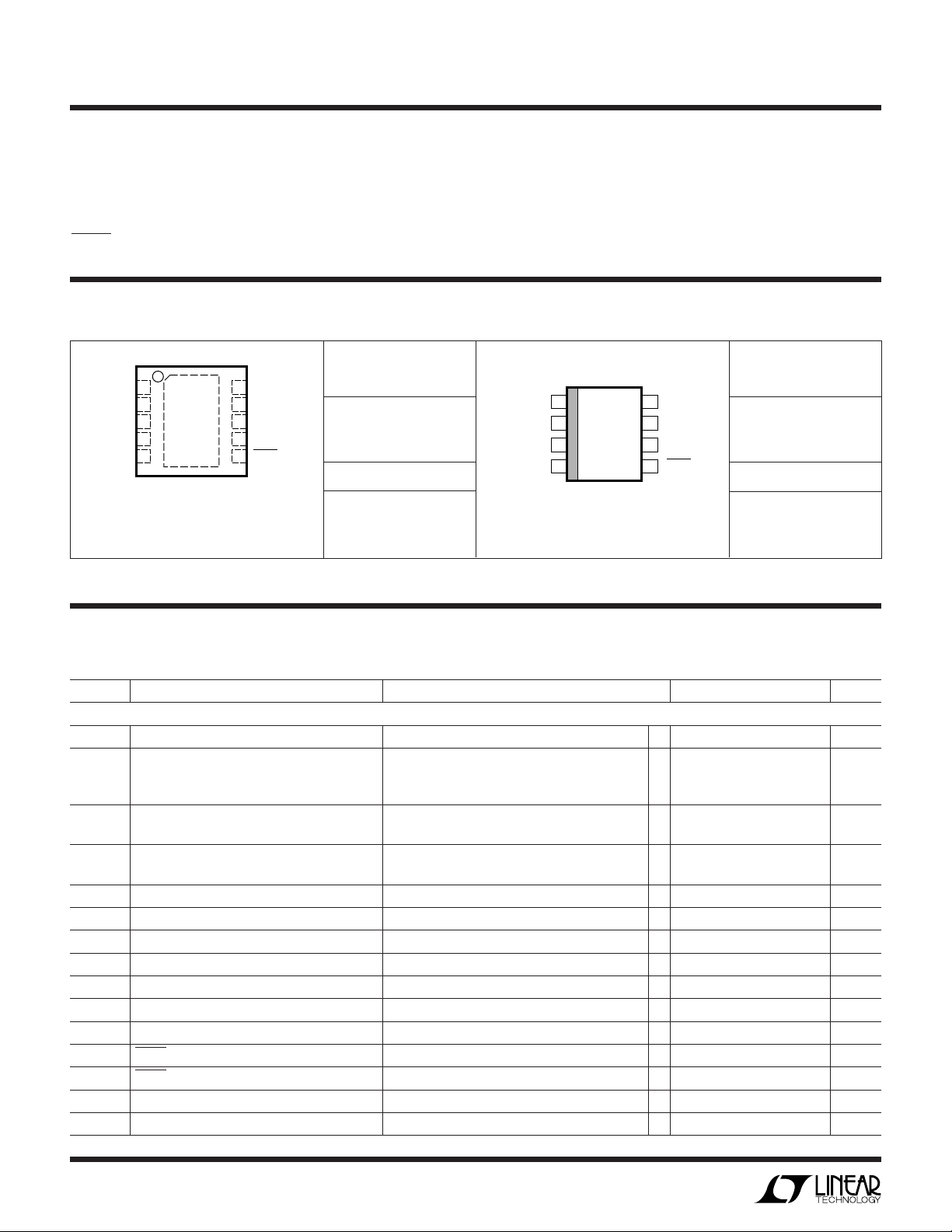
LTC4002-4.2
1
2
3
4
8
7
6
5
TOP VIEW
NTC
SENSE
BAT
CHRG
COMP
V
CC
GATE
GND
S8 PACKAGE
8-LEAD PLASTIC SO
TOP VIEW
11
DD PACKAGE
10-LEAD (3mm × 3mm) PLASTIC DFN
10
9
6
7
8
4
5
3
2
1
NC
NTC
SENSE
BAT
CHRG
COMP
V
CC
GATE
PGND
SGND
WW
W
ABSOLUTE AXI U RATI GS
U
(Note 1)
Supply Voltage (VCC) .............................................. 24V
GATE .................................................. (VCC –8V) to V
CC
BAT, SENSE .............................................. –0.3V to 14V
CHRG, COMP, NTC ..................................... – 0.3V to 8V
UUW
PACKAGE/ORDER I FOR ATIO
ORDER PART
NUMBER
LTC4002EDD-4.2
DD PART MARKING
T
= 125°C, θJA = 43°C/W
JMAX
EXPOSED PAD IS GND (PIN 11)
MUST BE SOLDERED TO PCB
Consult LTC Marketing for parts specified with wider operating temperature ranges.
LAGG
Operating Temperature Range (Note 2) .. – 40°C to 85°C
Storage Temperature Range ................. –65°C to 150°C
Lead Temperature (Soldering, 10 sec).................. 300°C
ORDER PART
NUMBER
LTC4002ES8-4.2
S8 PART MARKING
T
= 125°C, θJA = 110°C/W
JMAX
400242
ELECTRICAL CHARACTERISTICS
temperature range, otherwise specifications are at TA = 25°C. VCC = 10V unless otherwise noted.
SYMBOL PARAMETER CONDITIONS MIN TYP MAX UNITS
DC Characteristics
V
CC
I
CC
V
BAT
V
SNS(CHG)
V
SNS(TRKL)
V
TRKL
V
UV
∆V
UV
V
MSD
V
ASD
I
COMP
I
CHRG
V
CHRG
R
EOC
t
TIMER
2
VCC Supply Voltage ● 4.7 24 V
VCC Supply Current Current Mode 3 5 mA
Battery Regulated Float Voltage 5V ≤ VCC ≤ 24V (Note 2) 4.168 4.2 4.232 V
Constant Current Sense Voltage 3V ≤ V
Trickle Current Sense Voltage V
Trickle Charge Threshold Voltage V
VCC Undervoltage Lockout Threshold Voltage VCC Rising 3.9 4.2 4.5 V
VCC Undervoltage Lockout Hysteresis Voltage 200 mV
Manual Shutdown Threshold Voltage COMP Pin Falling 200 360 500 mV
Automatic Shutdown Threshold Voltage VCC – V
COMP Pin Output Current V
CHRG Pin Weak Pull-Down Current V
CHRG Pin Output Low Voltage I
End-of-Charge Ratio V
Charge Time Accuracy 10 %
The ● denotes the specifications which apply over the full operating
Shutdown Mode 3 5 mA
Sleep Mode 10 20 µA
● 4.158 4.242 V
≤ 4V (Note 3) 0°C ≤ TA ≤ 85°C ● 93 100 107 mV
BAT
= 0V (Note 3) 5 10 15 mV
BAT
Rising 2.75 2.9 3.05 V
BAT
BAT
= 1.2V 100 µA
COMP
= 1V 15 25 35 µA
CHRG
= 1mA 0.15 0.3 V
CHRG
SNS(EOC)/VSNS(CHG)
–40°C ≤ T
≤ 85°C ● 90 110 mV
A
250 mV
10 25 32 %
400242i
Page 3
LTC4002-4.2
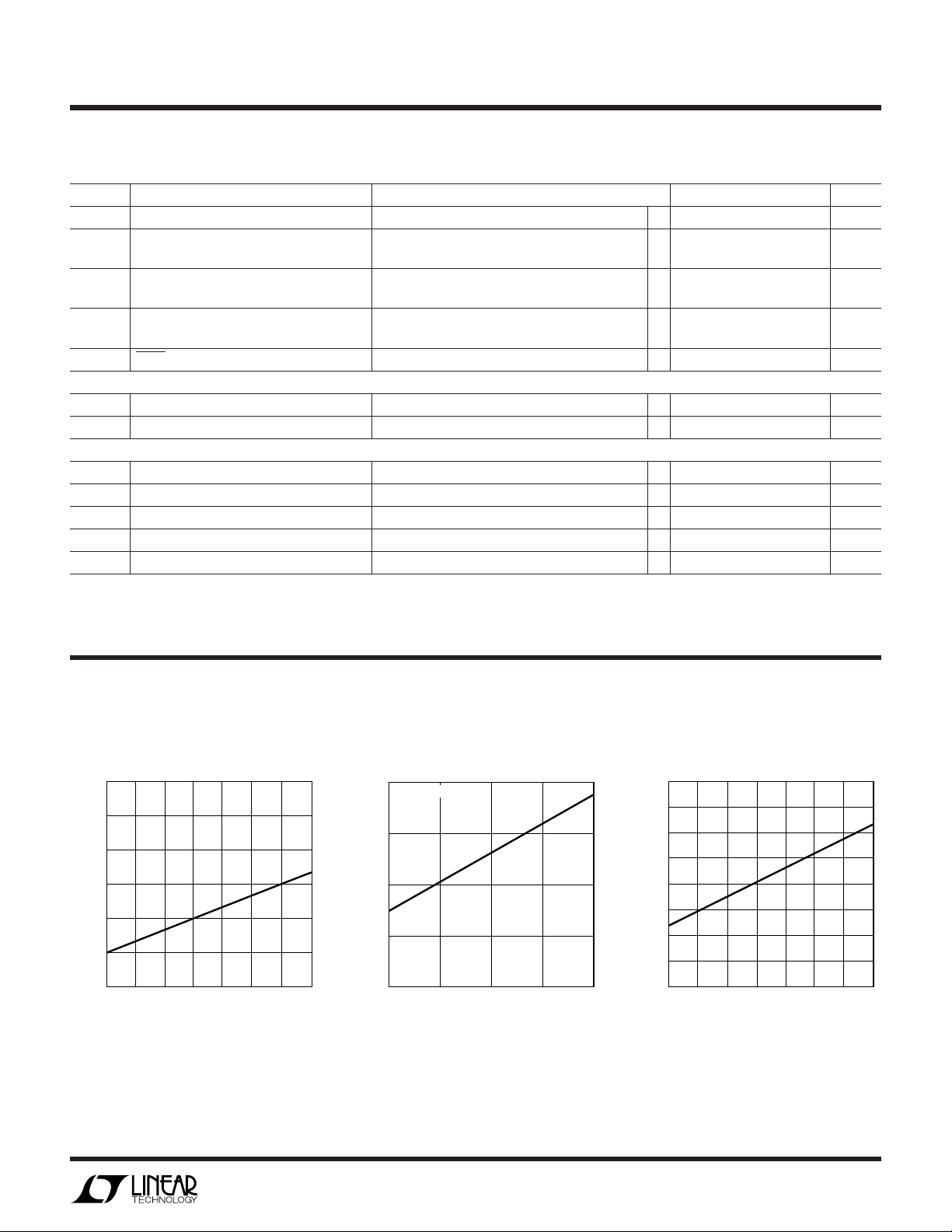
TEMPERATURE (°C)
–50
f
OSC
(kHz)
25
400242 G03
500
–25 0 50
450
550
75 100 125
ELECTRICAL CHARACTERISTICS
The ● denotes the specifications which apply over the full operating
temperature range, otherwise specifications are at TA = 25°C. VCC = 10V unless otherwise noted.
SYMBOL PARAMETER CONDITIONS MIN TYP MAX UNITS
I
NTC
V
NTC-HOT
V
NTC-COLD
∆V
RECHRG
I
LEAK
Oscillator
f
OSC
DC Maximum Duty Cycle 100 %
Gate Drive
t
r
t
f
∆V
GATE
∆V
GATEHI
∆V
GATELO
Note 1: Absolute Maximum Rating are those values beyond which the life
of a device may be impaired.
NTC Pin Output Current V
NTC Pin Threshold Voltage (Hot) V
= 0.85V ● 75 85 95 µA
NTC
Falling ● 340 355 370 mV
NTC
Hysteresis 25 mV
NTC Pin Threshold Voltage (Cold) V
Rising ● 2.428 2.465 2.502 V
NTC
Hysteresis 170 mV
Recharge Battery Voltage Offset from Full V
BAT(FULLCHARGED)
– V
RECHRG
, V
Falling 100 150 200 mV
BAT
Charged Battery Voltage
CHRG Pin Leakage Current V
= 8V, Charging Stops 1 µA
CHRG
Switching Frequency 450 500 550 kHz
Rise Time C
Fall Time C
Output Clamp Voltage VCC – V
Output High Voltage ∆V
Output Low Voltage ∆V
= 2000pF, 10% to 90% 20 ns
GATE
= 2000pF, 90% to 10% 50 ns
GATE
, VCC ≥ 9V ● 8V
GATE
GATEHI
GATELO
= VCC – V
= VCC – V
, VCC ≥ 7V ● 0.3 V
GATE
, VCC ≥ 7V ● 4.5 V
GATE
Note 2: The LTC4002-4.2 is tested with Test Circuit 1.
Note 3: The LTC4002-4.2 is tested with Test Circuit 2.
UW
TYPICAL PERFOR A CE CHARACTERISTICS
Supply Current vs Temperature Supply Current vs V
4.0
3.5
(mA)
CC
I
3.0
2.5
–50
–25 0
50 100 125
25 75
TEMPERATURE (°C)
400242 G01
(mA)
CC
I
4
3
2
CURRENT MODE
5
10
15
VCC (V)
CC
20
TA = 25°C, VCC = 10V unless otherwise noted.
Oscillator Frequency
vs Temperature
25
400242 G02
400242i
3
Page 4
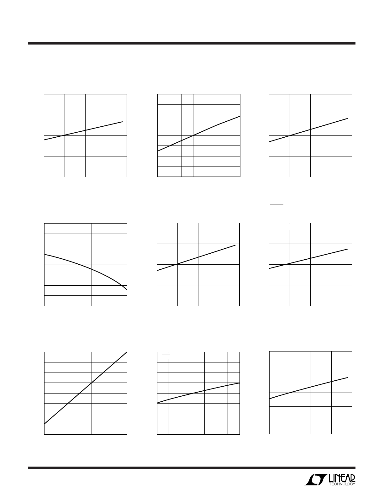
LTC4002-4.2
VCC (V)
5
22
I
CHRG
(µA)
25
28
10 15 20 25
400242 G11
V
CHRG
= 8V
UW
TYPICAL PERFOR A CE CHARACTERISTICS
TA = 25°C, VCC = 10V unless otherwise noted.
Oscillator Frequency vs V
510
(kHz)
500
OSC
f
490
5
10
VCC (V)
Trickle Charge Voltage
vs Temperature
3.0
(V)
2.9
TRKL
V
Current Mode Sense Voltage
CC
15
20
25
400242 G04
vs Temperature
104
V
= 4V
BAT
(mV)
100
SNS
V
96
–25 0 50
–50
25
TEMPERATURE (°C)
75 100 125
400242 G05
Trickle Charge Voltage
vs V
CC
3.0
V
= 4V
BAT
(V)
2.9
TRKL
V
Current Mode Sense Voltage
vs V
CC
102
V
= 4V
BAT
(mV)
100
SNS
V
98
5
10
15
VCC (V)
CHRG Pin Output Low Voltage
vs V
CC
150
I
= 1mA
LOAD
(mV)
140
CHRG
V
20
25
400242 G04
2.8
–25 0 50
–50
25
TEMPERATURE (°C)
75 100 125
400242 G07
CHRG Pin Output Low Voltage
vs Temperature
180
I
= 1mA
LOAD
(mV)
140
CHG
V
100
–25 0 50
–50
4
25
TEMPERATURE (°C)
75 100 125
400242 G10
2.8
5
10
15
VCC (V)
CHRG Pin Weak Pull-Down
Current vs Temperature
29
V
= 8V
CHRG
(µA)
25
CHRG
I
21
–25 0 50
–50
25
TEMPERATURE (°C)
20
400242 G08
75 100 125
400242 G23
25
130
5
10
15
VCC (V)
20
25
400242 G09
CHRG Output Pin Weak Pull-Down
Current vs V
CC
400242i
Page 5
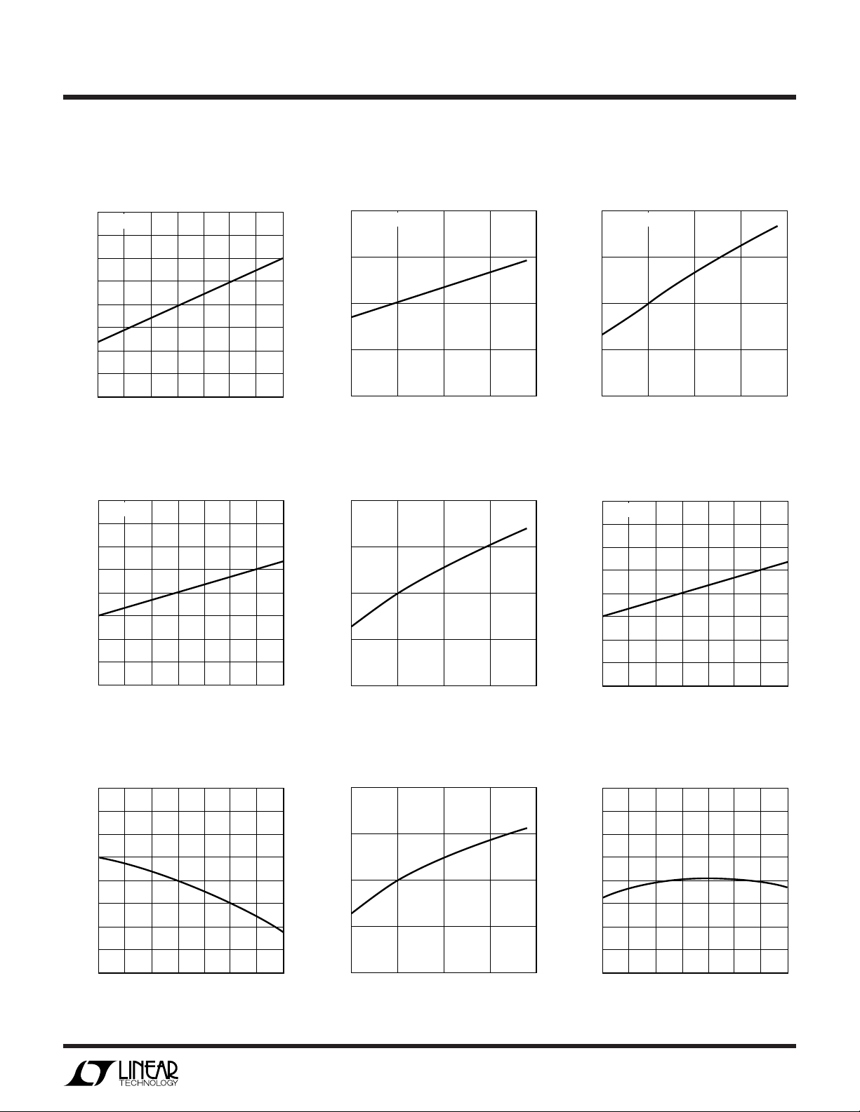
TEMPERATURE (°C)
–50
I
NTC
(µA)
25
400242 G17
85
–25 0 50
81
89
75 100 125
V
NTC
= 0V
TEMPERATURE (°C)
–50
R
EOC
(%)
25
400242 G20
25
–25 0 50
21
29
75 100 125
UW
TYPICAL PERFOR A CE CHARACTERISTICS
LTC4002-4.2
TA = 25°C, VCC = 10V unless otherwise noted.
Trickle Charge Sense Voltage
vs Temperature
10.4
V
= 2.5V
BAT
(mV)
10.0
SNS
V
9.6
–25 0 50
–50
25
TEMPERATURE (°C)
COMP Pin Output Current
vs Temperature
104
V
= 0V
COMP
75 100 125
400242 G12
Trickle Charge Sense Voltage
vs V
CC
11
V
= 2.5V
BAT
(mV)
10
SNS
V
9
5
10
15
V
(V)
CC
NTC Pin Output Current
vs V
CC
86
V
= 0V
NTC
COMP Pin Output Current
vs V
CC
102
V
= 0V
COMP
(µA)
100
COMP
I
20
25
400242 G13
98
5
10
15
VCC (V)
20
25
400242 G14
NTC Pin Output Current
vs Temperature
(µA)
100
COMP
I
96
–25 0 50
–50
25
TEMPERATURE (°C)
75 100 125
400242 G15
Recharge Voltage Offset from Full
Charged Voltage vs Temperature
190
(mV)
150
RECHRG
∆V
110
–25 0 50
–50
25
TEMPERATURE (°C)
75 100 125
400242 G18
(µA)
85
NTC
I
84
5
10
15
VCC (V)
Recharge Voltage Offset from Full
Charged Voltage vs V
160
(mV)
150
RECHRG
∆V
140
5
10
CC
15
VCC (V)
20
25
400242 G16
End-of-Charge Ratio
vs Temperature
20
25
400242 G19
400242i
5
Page 6

LTC4002-4.2
UW
TYPICAL PERFOR A CE CHARACTERISTICS
TA = 25°C, VCC = 10V unless otherwise noted.
End-of-Charge Ratio
vs V
CC
29
(%)
25
EOC
R
21
5
U
PI FU CTIO S
10 15 20 25
VCC (V)
400242 G21
UU
(DFN/SO-8)
COMP (Pin 1/Pin 1): Compensation, Soft-Start and Shut-
down Control Pin. The COMP pin is the control signal of the
inner loop of the current mode PWM. Charging begins when
the COMP pin reaches 800mV. The recommended compensation components are a 0.47µF (or larger) capacitor and
a 2.2k series resistor. A 100µA current into the compen-
sation capacitor also sets the soft-start slew rate. Pulling
the COMP pin below 350mV will shut down the charger.
VCC (Pin 2/Pin 2): Positive Supply Voltage Input. VCC can
range from 4.7V to 24V. A 0.1µF or higher capacitor is
required at the V
pin with the lead length kept to a mini-
CC
mum. A 10µF low ESR capacitor is also required at the
source pins of the power P-channel MOSFET.
GATE (Pin 3/Pin 3): Gate Drive Output. Driver Output for
the P-Channel MOSFET. The voltage at this pin is internally
clamped to 8V below VCC, allowing a low voltage MOSFET
with gate-to-source breakdown voltage of 8V or less to be
used.
PGND, SGND, Exposed Pad, GND (Pins 4, 5, 11/4): IC
Ground.
CHRG (Pin 6/Pin 5): Open-Drain Charge Status Output.
When the battery is being charged, the CHRG pin is pulled
low by an internal N-channel MOSFET. When the charge
current drops to 25% of the full-scale current for more than
Undervoltage Lockout Threshold
vs Temperature
4.4
VCC RISING
(V)
4.2
UV
V
4.0
–25 0 50
–50
25
TEMPERATURE (°C)
75 100 125
400242 G22
120µs, the N-channel MOSFET turns off and a 25µA cur-
rent source is connected from the CHRG pin to GND. When
the timer runs out or the input supply is removed, the 25µA
current source is turned off and the CHRG pin becomes high
impedance.
BAT (Pin 7/Pin 6): Battery Sense Input. A bypass capacitor of 22µF is required to minimize ripple voltage. An
internal resistor divider, which is disconnected in sleep
mode, sets the final float voltage at this pin. If the battery
connection is opened when charging, an overvoltage
circuit will limit the charger output voltage to 10% above
the programmed float voltage.
When V
is within 250mV of VCC, the LTC4002-4.2 is
BAT
forced into sleep mode, dropping ICC to 10µA.
SENSE (Pin 8/Pin 7): Current Amplifier Sense Input. A sense
resistor, R
, must be connected between the SENSE
SENSE
and BAT pins. The maximum charge current is equal to
100mV/R
SENSE
.
NTC (Pin 9/Pin 8): NTC (Negative Temperature Coefficient)
Thermistor Input. With an external 10kΩ NTC thermistor
to ground, this pin senses the temperature of the battery
pack and stops the charger when the temperature is out of
range. When the voltage at this pin drops below 350mV at
400242i
6
Page 7

LTC4002-4.2
U
PI FU CTIO S
UU
(DFN/SO-8)
hot temperature or rises above 2.465V at cold temperature,
charging is suspended and the internal timer stops. The
CHRG pin output is not affected during this hold state. To
W
BLOCK DIAGRA
COMP
M1
100µA
V
CC
CLK:
I
I
L
SLOP
–
C
PWM
+
R
SLOP
R
IL
disable the temperature qualification function, ground the
NTC pin.
NC (Pin 10/NA): No Connect.
S
Q
R
R
DRIVER
20mV
+
+
–
C
EOC
–
100mV
+
+
–
CA
–
GATE
SENSE
CHRG
+
BAT
M2
VA
4.2V
–
+
M3
90µA
C
LB
2.9V
–
+
C
350mV
OV
UVLO
4.2V
+
C
SD
–
Q4
Q5
25µA
SD
LOGIC
C/10
STOP
NTC_DISABLE
UV
EOC
RQ
TEMP
C
C
COLD
RQ
4.62V
–
+
4.05V
–
2.465V
+
–
85µA
V
CC
NTC
–
GND
C
HOT
+
350mV
+
50mV
–
400242 BD
400242i
7
Page 8

LTC4002-4.2
TEST CIRCUITS
1.5V
COMP
Test Circuit 1
15V
–
LT1006
+
0V
100µA
LTC4002-4.2
SENSE
–
R
CA
BAT
+
SENSE
10Ω
V
BAT
400242 TC01
1.5V
COMP
15V
–
LT1006
+
0V
100µA
LTC4002-4.2
Test Circuit 2
–
CA
+
–
VA
+
4.2V
SENSE
BAT
400242 TC02
R
SENSE
10Ω
1mA
8
400242i
Page 9

OPERATIO
LTC4002-4.2
U
The LTC4002 is a constant current, constant voltage
Li-Ion battery charger controller that uses a current mode
PWM step-down (buck) switching architecture. The charge
current is set by an external sense resistor (R
across the SENSE and BAT pins. The final battery float
voltage is internally set to 4.2V. For batteries like lithiumion that require accurate final float voltage, the internal
2.465V reference, voltage amplifier and the resistor divider provide regulation with ±1% accuracy.
A charge cycle begins when the voltage at the VCC pin rises
above the UVLO level (4.2V) and is 250mV or more greater
than the battery voltage. At the beginning of the charge
cycle, if the battery voltage is less than 2.9V, the charger
goes into trickle charge mode. The trickle charge current
is internally set to 10% of the full-scale current. If the
battery voltage stays low for 30 minutes, the battery is
considered faulty and the charge cycle is terminated.
When the battery voltage exceeds 2.9V, the charger goes
into the full-scale constant current charge mode. In constant current mode, the charge current is set by the
external sense resistor R
reference; I
When the battery voltage approaches the programmed
float voltage, the charge current will start to decrease.
= 100mV/R
BAT
and an internal 100mV
SENSE
.
SENSE
SENSE
)
When the current drops to 25% of the full-scale charge
current, an internal comparator turns off the internal pulldown N-channel MOSFET at the CHRG pin, and connects
a weak current source to ground to indicate a near end-ofcharge condition.
An internal 3 hour timer determines the total charge time.
After a time out occurs, the charge cycle is terminated
and the CHRG pin is forced high impedance. To restart
the charge cycle, remove and reapply the input voltage or
momentarily shut the charger down. Also, a new charge
cycle will begin if the battery voltage drops below the
recharge threshold voltage of 4.05V.
When the input voltage is present, the charger can be shut
down (ICC = 3mA) by pulling the COMP pin low. When the
input voltage is not present, the charger goes into sleep
mode, dropping ICC to 10µA. This will greatly reduce the
current drain on the battery and increase the standby time.
A 10kΩ NTC (negative temperature coefficient) thermistor
can be connected from the NTC pin to ground for battery
temperature qualification. The charge cycle is suspended
when the temperature is outside of the 0°C to 50°C
window (with DALE NTHS-1206N02).
400242i
9
Page 10

LTC4002-4.2
WUUU
APPLICATIO S I FOR ATIO
Undervoltage Lockout (UVLO)
An undervoltage lockout circuit monitors the input voltage
and keeps the charger off until VCC rises above 4.2V and
at least 250mV above the battery voltage. To prevent
oscillation around the threshold voltage, the UVLO circuit
has 200mV of built-in hysteresis.
Trickle Charge and Defective Battery Detection
At the beginning of a charge cycle, if the battery voltage is
below 2.9V, the charger goes into trickle charge mode with
the charge current reduced to 10% of the full-scale current. If the low-battery voltage persists for 30 minutes, the
battery is considered defective, the charge cycle is terminated and the CHRG pin is forced to be high impedance.
Shutdown
The LTC4002 can be shut down by pulling the COMP pin
to ground which pulls the GATE pin high and turns off the
external P-channel MOSFET. When the COMP pin is released, the internal timer is reset and a new charge cycle
starts. In shutdown, the output of the CHRG pin is high
impedance and the quiescent current remains at 3mA.
Removing the input power supply will put the charger
into sleep mode. If the voltage at the VCC pin drops below
(V
+ 250mV) or below the UVLO level (4.2V), the
BAT
LTC4002-4.2 goes into a low current (I
= 10µA) sleep
CC
mode, reducing the battery drain current.
CHRG Status Output Pin
When a charge cycle starts, the CHRG pin is pulled to
ground by an internal N-channel MOSFET which is capable
of driving an LED. When the charge current drops to 25%
of the full-scale current for more than 120µs, the N-channel
MOSFET turns off and a weak 25µA current source to
ground is connected to the CHRG pin. This weak 25µA
pull-down remains until the timer ends the charge cycle,
or the charger is in manual shutdown or sleep mode.
After a time out occurs (charge cycle ends), the pin will go
into high impedance. By using two different value resistors, a microprocessor can detect three states from this
pin (charging, end-of-charge and charging stopped) see
Figure␣ 2.
To detect the charge mode, force the digital output pin,
OUT, high and measure the voltage at the CHRG pin. The
N-channel MOSFET will pull the pin low even with a 2k
pull-up resistor. Once the charge current drops to 25% of
the full-scale current, the N-channel MOSFET is turned off
and a 25µA current source is connected to the CHRG pin.
The IN pin will then be pulled high by the 2k resistor
connected to OUT. Now force the OUT pin into a high
impedance state, the current source will pull the pin low
through the 400k resistor. When the internal timer has
expired, the CHRG pin changes to a high impedance state
and the 400k resistor will then pull the pin high to indicate
the charging has stopped.
10
V
CC
400k
2k
Figure 2. Microprocessor Interface
V
DD
µPROCESSORLTC4002-4.2
OUTCHRG
IN
400242 F02
400242i
Page 11

WUUU
APPLICATIO S I FOR ATIO
LTC4002-4.2
Gate Drive
The LTC4002-4.2 gate driver can provide high transient
currents to drive the external pass transistor. The rise and
fall times are typically 20ns and 50ns respectively when
driving a 2000pF load, which is typical for a P-channel
MOSFET with R
A voltage clamp is added to limit the gate drive to 8V below
VCC. For example, if VCC is 10V then the GATE output will
pull down to 2V max. This allows low voltage P-channel
MOSFETs with superior R
transistor thus increasing efficiency.
Stability
Both the current loop and the voltage loop share a common, high impedance, compensation node (COMP pin). A
series capacitor and resistor on this pin compensates both
loops. The resistor is included to provide a zero in the loop
response and boost the phase margin.
The compensation capacitor also provides a soft-start
function for the charger. Upon start-up, the COMP pin
voltage will quickly rise to 0.05V, due to the 2.2k series
resistor, then ramp at a rate set by the internal 100µA pull-
up current source and the external capacitor. Battery
charge current starts ramping up when the COMP pin
voltage reaches 0.8V and full current is achieved with the
COMP pin at 1.3V. With a 0.47µF capacitor, time to reach
full charge current is about 235ms. Capacitance can be
increased up to 1µF if a longer start-up time is needed.
in the range of 50mΩ.
DS(ON)
DS(ON)
to be used as the pass
Automatic Battery Recharge
After the 3 hour charge cycle is completed and both the
battery and the input power supply (wall adapter) are still
connected, a new charge cycle will begin if the battery
voltage drops below 4.05V due to self-discharge or external loading. This will keep the battery capacity at more than
80% at all times without manually restarting the charge
cycle.
Battery Temperature Detection
A negative temperature coefficient (NTC) thermistor
located close to the battery pack can be used to monitor
battery temperature and will not allow charging unless the
battery temperature is within an acceptable range.
Connect a 10kΩ thermistor (DALE NTHS-1206N02) from
the NTC pin to ground. If the temperature rises to 50°C, the
resistance of the NTC will be approximately 4.1kΩ. With
the 85µA pull-up current source, the Hot temperature
voltage threshold is 350mV. For Cold temperature, the
voltage threshold is set at 2.456V which is equal to 0°C
(R
≅ 28.4kΩ) with 85µA of pull-up current. If the
NTC
temperature is outside the window, the GATE pin will be
pulled up to VCC and the timer frozen while the output
status at the CHRG pin remains the same. The charge cycle
begins or resumes once the temperature is within the
acceptable range. Short the NTC pin to ground to disable
the temperature qualification feature.
400242i
11
Page 12

LTC4002-4.2
WUUU
APPLICATIO S I FOR ATIO
Input and Output Capacitors
Since the input capacitor is assumed to absorb all input
switching ripple current in the converter, it must have an
adequate ripple current rating. Worst-case RMS ripple current is approximately one-half of output charge current.
Actual capacitance value is not critical. Solid tantalum
capacitors have a high ripple current rating in a relatively
small surface mount package, but caution must be used
when tantalum capacitors are used for input bypass. High
input surge currents can be created when the adapter is
hot-plugged to the charger and solid tantalum capacitors
have a known failure mechanism when subjected to very
high turn-on surge currents. Selecting the highest possible voltage rating on the capacitor will minimize problems. Consult with the manufacturer before use.
The selection of output capacitor C
mined by the ESR required to minimize ripple voltage and
load step transients. The output ripple ∆V
mately bounded by:
∆≤∆ +
V I ESR
OUT L
Since ∆IL increases with input voltage, the output ripple is
highest at maximum input voltage. Typically, once the ESR
requirement is satisfied, the capacitance is adequate for
filtering and has the necessary RMS current rating.
1
fC
8
OSC OUT
is primarily deter-
OUT
is approxi-
OUT
Switching ripple current splits between the battery and the
output capacitor depending on the ESR of the output capacitor and the battery impedance. EMI considerations
usually make it desirable to minimize ripple current in the
battery leads. Ferrite beads or an inductor may be added
to increase battery impedance at the 500kHz switching
frequency. If the ESR of the output capacitor is 0.2Ω and
the battery impedance is raised to 4Ω with a bead or inductor, only 5% of the current ripple will flow in the battery.
Design Example
As a design example, take a charger with the following
specifications: V
1.5A, f
First, calculate the SENSE resistor :
R
Choose the inductor for about 65% ripple current at the
maximum VIN:
L
Selecting a standard value of 6.8µH results in a maximum
ripple current of :
∆=
= 500kHz, see Figure 1.
OSC
= 100mV/1.5A = 68mΩ
SENSE
500 0 65 1 5
()()()
L
500 6 8
()
= 5V to 24V, V
IN
4
V
kHz A
..
V
4
kHz H
.
µ
()
= 4V nominal, I
BAT
4
1
V
1
–.
4
–.
24
=µ
24
V
V
=I
980 4
V
6 838
BAT
H=
mA
=
12
400242i
Page 13

WUUU
APPLICATIO S I FOR ATIO
LTC4002-4.2
Next, choose the P-channel MOSFET. The Si6435ADQ in
a TSSOP-8 package with R
(max) offers a small solution. The maximum power dissipation with V
temperature is:
1 5 55 4
()
P
=
D
TJ = 50°C + (0.099W)(65°C/W) = 56.5°C
CIN is chosen for an RMS current rating of about 0.8A at
85°C. The output capacitor is chosen for an ESR similar to
the battery impedance of about 100mΩ. The ripple voltage
on the BAT pin is:
V
OUT RIPPLE
()
C1: Taiyo Yuden TMK325BJ106MM
C2: Taiyo Yuden JMK325BJ226MM
L1: TOKO B952AS-6R8N
The Schottky diode D2 shown in Figure 1 conducts current
when the pass transistor is off. In a low duty cycle case, the
current rating should be the same or higher than the
charge current. Also it should withstand reverse voltage as
high as VIN.
= 5V and V
IN
2
.
AmV
()()
V
5
∆
=
098 01
()
=
DS(ON)
Ω
I ESR
LMAX
()
2
..
A
()
2
= 42mΩ (nom), 55mΩ
= 4V at 50°C ambient
BAT
.
=
0 099
W
()
Ω
=
49
mV
Board Layout Suggestions
When laying out the printed circuit board, the following
considerations should be taken to ensure proper operation of the LTC4002-4.2.
GATE pin rise and fall times are 20ns and 50ns respectively
(with C
diode, pass transistor and the input bypass capacitor
traces should be kept as short as possible. The positive
side of the input capacitor should be close to the source of
the P-channel MOSFET; it provides the AC current to the
pass transistor. The connection between the catch diode
and the pass transistor should also be kept as short as
possible. The SENSE and BAT pins should be connected
directly to the sense resistor (Kelvin sensing) for best
charge current accuracy.
The compensation capacitor connected at the COMP pin
should return to the ground pin of the IC or as close to it
as possible. This will prevent ground noise from disrupting the loop stability. The ground pin also works as a heat
sink, therefore use a generous amount of copper around
the ground pin. This is especially important for high V
and/or high gate capacitance applications.
= 2000pF). To minimize radiation, the catch
GATE
CC
400242i
13
Page 14

LTC4002-4.2
PACKAGE DESCRIPTIO
U
DD Package
10-Lead Plastic DFN (3mm × 3mm)
(Reference LTC DWG # 05-08-1699)
0.675 ±0.05
3.50 ±0.05
1.65 ±0.05
(2 SIDES)2.15 ±0.05
PACKAGE
OUTLINE
0.25 ± 0.05
RECOMMENDED SOLDER PAD PITCH AND DIMENSIONS
PIN 1
TOP MARK
(SEE NOTE 5)
0.200 REF
NOTE:
1. DRAWING TO BE MADE A JEDEC PACKAGE OUTLINE M0-229 VARIATION OF (WEED-2).
CHECK THE LTC WEBSITE DATA SHEET FOR CURRENT STATUS OF VARIATION ASSIGNMENT
2. ALL DIMENSIONS ARE IN MILLIMETERS
3. DIMENSIONS OF EXPOSED PAD ON BOTTOM OF PACKAGE DO NOT INCLUDE
MOLD FLASH. MOLD FLASH, IF PRESENT, SHALL NOT EXCEED 0.15mm ON ANY SIDE
4. EXPOSED PAD SHALL BE SOLDER PLATED
5. SHADED AREA IS ONLY A REFERENCE FOR PIN 1 LOCATION ON THE
TOP AND BOTTOM OF PACKAGE
0.50
BSC
2.38 ±0.05
(2 SIDES)
3.00 ±0.10
(4 SIDES)
0.75 ±0.05
1.65 ± 0.10
(2 SIDES)
0.00 – 0.05
R = 0.115
TYP
2.38 ±0.10
(2 SIDES)
BOTTOM VIEW—EXPOSED PAD
106
15
0.50 BSC
0.38 ± 0.10
0.25 ± 0.05
(DD10) DFN 0403
14
400242i
Page 15

PACKAGE DESCRIPTIO
.050 BSC
U
S8 Package
8-Lead Plastic Small Outline (Narrow .150 Inch)
(Reference LTC DWG # 05-08-1610)
.189 – .197
.045 ±.005
(4.801 – 5.004)
8
NOTE 3
7
LTC4002-4.2
5
6
.245
MIN
.030 ±.005
TYP
RECOMMENDED SOLDER PAD LAYOUT
.010 – .020
(0.254 – 0.508)
.008 – .010
(0.203 – 0.254)
NOTE:
1. DIMENSIONS IN
2. DRAWING NOT TO SCALE
3. THESE DIMENSIONS DO NOT INCLUDE MOLD FLASH OR PROTRUSIONS.
MOLD FLASH OR PROTRUSIONS SHALL NOT EXCEED .006" (0.15mm)
× 45°
.016 – .050
(0.406 – 1.270)
INCHES
(MILLIMETERS)
.160
±.005
.228 – .244
(5.791 – 6.197)
0°– 8° TYP
.053 – .069
(1.346 – 1.752)
.014 – .019
(0.355 – 0.483)
TYP
.150 – .157
(3.810 – 3.988)
NOTE 3
1
3
2
4
.004 – .010
(0.101 – 0.254)
.050
(1.270)
BSC
SO8 0303
400242i
15
Page 16

LTC4002-4.2
TYPICAL APPLICATIO
U
Single Cell 4.2V, 2A Li-Ion Battery Charger
100k
1/2 Si9933ADY
V
IN
5V TO 12V
B330-13
Li-Ion
BATTERY
400242 TA01
C1
10µF
CER
2.2k
0.1µF
CER
0.47µF
LTC4002ES8-4.2
5
CHRG
COMP
NTC GND
84
T
V
CC
10k
NTC
2
3
GATE
7
SENSE
61
BAT
NTC: DALE NTHS-1206N02
1/2 Si9933ADY
L1
6.8µH
R
SENSE
50mΩ
C2
+
22µF
CER
RELATED PARTS
PART NUMBER DESCRIPTION COMMENTS
LTC1732/LTC4050 Constant Voltage/Constant Current Li-Ion Linear Standalone Battery Charger, No uC or Firmware Required, Auto
Battery Chargers Recharge of Low Battery, 10-Pin MSOP, Input Supply Detection
LTC1733 Li-Ion Battery Charger with Termal Regulation Standalone Charger, Constant-Current/Constant-Voltage/
Constant-Temperature, Integrated MOSFET, No External Sense
Resistor or Blocking Diodes
LTC1734/LTC1734L SOT-23 Li-Ion Battery Chargers Need Only Two External Components, Monitors Charge Current, No
Reverse Diode or Sense Resistor Required, 50mA to 700mA
LTC1980 Combination Battery Charger and DC/DC Converter Wall Adapter May Be Above or Below Battery Voltage, Standalone,
1-, 2-Cell Li-Ion, Also for Charging NiMH and NiCd Batteries
LTC4006/LTC4007 4A Multiple Cell Li-Ion, NiCd, NiMH, Lead Acid 6V ≤ VIN ≤ 28V, High Efficiency ≥90%, V
LTC4008 Battery Chargers Digital Interface I/O, Small Inductor
LTC4052/LTC1730 Integrated Pulse Chargers for a 1-Cell Li-Ion Battery 0.35Ω Internal N-FET Requires No Blocking Diode,
Current Limit for Safety
LTC4053 USB Compatible Li-Ion Linear Battery Charger Charges from USB Input or AC/DC, 100mA/500mA Up to 1.25A,
Thermal Regulation, Fully Integrated
LTC4054 Standalone Linear Li-Ion Battery Charger Thermal Regulation Prevents Overheating, C/10 Termination,
with Integrated Pass Transistor in ThinSOT
TM
C/10 Indicator
LTC4056 Standalone SOT-23 Li-Ion Linear Battery Charger Charge Termination Included, ICH ≤ 700mA, 8-Lead ThinSOT Package
LTC4412 Low Loss PowerPathTM Controller in ThinSOT Automatic Switching Between DC Sources, Simplified Load Sharing
PowerPath and ThinSOT are trademarks of Linear Technology Corporation.
OUT
≤ 28V,
16
Linear Technology Corporation
1630 McCarthy Blvd., Milpitas, CA 95035-7417
(408) 432-1900 ● FAX: (408) 434-0507
●
www.linear.com
400242i
LT/TP 0603 1K PRINTED IN USA
LINEAR TECHNOLOGY CORPORATION 2003
 Loading...